
Nanoarchitectonics: a new materials horizon for nanotechnology
Katsuhiko
Ariga
*,
Qingmin
Ji
,
Waka
Nakanishi
,
Jonathan P.
Hill
and
Masakazu
Aono
*
World Premier International Center for Materials Nanoarchitectonics (WPI-MANA), National Institute for Materials Science (NIMS), 1-1 Namiki, Tsukuba 305-0044, Japan. E-mail: ARIGA.Katsuhiko@nims.go.jp; AONO.Masakazu@nims.go.jp; Fax: +81-29-860-4832; Tel: +81-29-860-4597
First published on 12th February 2015
Abstract
Nanoarchitectonics is introduced as a rising tide within current nanomaterials science. Physical phenomena operate quite differently at the nanoscale (compared to in the macroscopic and microscopic regimes) with behaviours of nanoscopic objects being strongly influenced by thermal/statistical fluctuations and mutual interactions between components. Nanoarchitectonic methods, and the materials that they produce, contrast strongly with those of conventional nanotechnology. In this review, to illustrate the potential of nanoarchitectonics for future technologies, examples of nanoarchitectonics are introduced which are categorized as (i) atomic or molecular manipulation as a route to leading nanotechnologies, (ii) materials creation in the realization of materials nanoarchitectonics, and (iii) advanced device materials.
 Katsuhiko Ariga | Katsuhiko Ariga received his PhD degree from Tokyo Institute of Technology. He is currently the Director of Supermolecules Group and Principal Investigator of World Premier International (WPI) Research Centre for Materials Nanoarchitectonics (MANA), the National Institute for Materials Science (NIMS). Dr Ariga has been a Fellow of the Royal Society of Chemistry (FRSC) since 2013. |
 Qingmin Ji | Qingmin Ji earned her PhD (2005) in chemistry from the University of Tsukuba. She commenced work as a post-doctoral fellow at National Institute for Materials Science (NIMS) in 2006 and became MANA scientist at the World Premier International (WPI) Research Centre for Materials Nanoarchitectonics (MANA) in 2011. Her research currently focuses on the formation of layer-by-layer films and the application of mesoporous structures as delivery systems. |
 Waka Nakanishi | Waka Nakanishi received her PhD (2005) degree from the University of Tokyo. She became a research associate in 2005 and an assistant professor in 2007 at Chiba University. Then she became a lecturer in Tohoku University in 2008. In 2013 she joined the NIMS as a permanent staff. Her major interests are synthesis of conjugated molecules and control of their structures for the application of materials science to biology. |
 Jonathan P. Hill | Jonathan P. Hill is currently a MANA Scientist and sub-group leader of the Supermolecules Group at the Research Centre for Materials Nanoarchitectonics, National Institute for Materials Science. His current research interests include synthesis of tetrapyrroles, phthalocyanines and pyrazinacenes, their properties at the single molecular level or when contained in supramolecular manifolds, and unusual methods for preparing organic and hybrid nanomaterials in their bulk and at surfaces. |
 Masakazu Aono | Masakazu Aono received his Ph. D degree from the University of Tokyo in 1972. Subsequently, he became a Research Staff Member of the National Institute for Research in Inorganic Materials (NIRIM). In 1986, he moved to RIKEN Institute as a Chief Scientist and organized the Surface and Interface Laboratory there until 2002. From 1996 to 2002, he was also a Professor at Osaka University. In 2002, he joined the National Institute for Materials Science (NIMS) as the Director General of the Nanomaterials Laboratory. He assumed the Director General of the International Center for Materials Nanoarchitectonics (MANA) in 2007; MANA is a World Premier International Center supported by Japan's Ministry of Education, Culture, Science and Technology (MEXT). |
1. Introduction
1.1. What is on the nanomaterials horizon?
In the design, synthesis, and fabrication of functional materials, control of their nanometer-level (nanoscale) structures is of substantial importance. There is a wide range of excellent examples of materials fabrications which permit impressive nanoscale structural precision, and the related research areas have become extremely productive.1 The resulting nanomaterials and/or nanostructured materials are widely used for practical applications in high demand fields such as energy & environmental sciences, device technology, and biomedical areas.2 Although these aspects represent substantial progress, research efforts have become diversified and dispersed according to the requirements of those fields. Thus, it is now appropriate to introduce a new concept in order to stimulate creativity in the nanomaterials field. Quite a similar situation existed twenty or so years ago when the development of techniques including advanced microscopies and microfabrication methods provided access to the nanoscopic world. Consequently, a variety of high level scientific studies and the development of technologies based on nanosized objects could be achieved. Based on these initial investigations and fabrications, the concept of nanotechnology was eventually coined as an umbrella term thus establishing the eponymous dynamic and productive research field. Richard Feynman famously foretold the field of nanotechnology with his words, “There's plenty of room at the bottom,” which anticipated the current trends in the science of nanosized objects. Now nanotechnology is an established field and it would be timely to propose a novel concept towards its development, and this concept is nanoarchitectonics,3 which is here introduced as a rising tide within the current nanomaterials field.1.2. Nano is not an extension of micro
It might appear obvious that if we continuously miniaturize scientific tools and fabrication techniques, we may finally become the architects of nanosized objects. However, although we can achieve microscale constructions by miniaturizing existing fabrication techniques, the same strategies may not always be useful for the fabrication of specific nanostructures. Thermal and statistical fluctuations do not much affect microscale objects and their properties and behaviour can be predicted based on an extension of the properties of macroscale objects. Thus, simple miniaturization of available fabrication tools has led directly to the introduction of microtechnological devices and the successful implementation of microfabrication technologies during the course of the continuing development of silicon-based devices.Physical phenomena occurring at the nanoscale can operate quite differently from those in the microscopic regime. The behaviours of nanoscopic objects are strongly affected by thermal/statistical fluctuations and mutual interactions between components so that the cause and effect cannot be represented by simple input and output signals.4 In fact, unexpected interactions may occur. For instance, a stimulus applied to a selected target at the nanoscale may also affect the surrounding moieties or components of a nanoscale material causing additional mutual interactions. Therefore, when preparing nanostructured materials it is necessary to consider the fine structures and compositions of nanosized components and any inter-component interactions. For this reason, a more concerted approach to a nanomaterial construction or assembly may be advantageous. Such an approach can be represented by the nanoarchitectonic concept which is anticipated to be an advanced fabrication methodology in the nanoscopic arena.
From another point-of-view, the fabrication of nanomaterials differs fundamentally from materials of macroscopic dimensions. For the latter, selected materials are fabricated into the required shape for use as components. In contrast, component creation and structural fabrication cannot be separate processes in nanoscale fabrications. The synthesis of structures from nanosized unit-components often leads to creation of novel materials with unexpected properties since mutual interactions between components and structure-specific effects make a large contribution to the properties of the resulting materials. Structural fabrication by nanoarchitectonics corresponds to the creation of a new material. Therefore, it can be further called materials nanoarchitectonics.
In terms of materials preparation and properties, nano is not a direct extension of micro, and an architectonic concept is required rather than a fabrication technology. Fabrication of functional structures and creation of functional materials based on the concept of nanoarchitectonics require the harmonization of various techniques and phenomena including control at atomic or molecular levels, fabrication based on chemical reactions, structural control based on application of various physical stimuli, and self-assembly/organization. Here, a novel strategy for theoretical modelling that includes harmonization phenomena is also necessary.
1.3. A paradigm shift from nanotechnology to nanoarchitectonics
As mentioned previously, the success of nanotechnology was anticipated by the foresight of Feynman. Another important conceptual proposal was also made by Kim Eric Drexler who proposed molecular nanotechnology and bottom-up-type structural construction in his book entitled Nanosystems: Molecular Machinery, Manufacturing and Computation. At around the same time, significant technological progress was made on observation tools such as electron microscopies and scanning tunneling microscopy (STM). Apart from those observational techniques, fabrication at the nanoscale was also demonstrated through artificial arrangements of Xe atoms (to write ‘IBM’) using an STM apparatus. Additionally, US president Bill Clinton made a declaration aimed at the promotion of nanotechnology in 2001 (the National Nanotechnology Initiative). The nanotech concept helped to promote science and technology so that simply proposing a novel concept can be seen as being as important as any individual scientific finding and technological innovation. With this in mind, we should consider the next post-nanotech idea.In the “post-nanotechnology” era, nanoarchitectonics can be seen as a rising tide on the horizon of current materials research. This terminology was first proposed and defined by Masakazu Aono at the 1st International Symposium on Nanoarchitectonics Using Suprainteractions in 2000 in Tsukuba, Japan.3 Almost concurrently (in 2001), the term was also used at the Interfacial Nanoarchitectonics Centre in the National Institute of Advanced Industrial Science and Technology in Tsukuba, Japan (Toshimi Shimizu). The terminology has also been used in the title of a scientific publication by Stefan Hecht.5 Subsequently, Aono established the World Premium International Research Center for Materials Nanoarchitectonics (WPI-MANA) in 2007 (ref. 6) and the nanoarchitectonics terminology has been variously used as the subject of journal special themed issues and international conferences. The application of the nanoarchitectonics concept in various research fields including nanomaterial development,7 nanostructure fabrication,8 and application-oriented science such as sensing9 and biomedical usages10 has been continuous.
Reported trends clearly imply that nanoarchitectonics is rising over the horizon of research on nanotechnology and materials science. In the following sections of this review, to illustrate the potential of nanoarchitectonics for future technologies, examples of nanoarchitectonics products are introduced which are categorized as (i) atomic and molecular manipulation as a bridge to fore-front nanotechnology, (ii) materials creation for realization of materials nanoarchitectonics, and (iii) advanced device materials.
2. Examples of nanoarchitectonics
2.1. Atom/molecule manipulation
Manipulation of atoms and molecules is a fundamental construction mode in nanoarchitectonics permitting synthesis of functional materials systems and devices. A typical example lies in the development of an atomic switch (Fig. 1).11 Since nanometer-sized metal atom clusters make highly conductive channels, manipulation of only a few atoms can be used to toggle on a switching device (even in computing applications). Application of a negative voltage to a Pt electrode at 1 nm separation from a Ag2S electrode results in a miniscule tunneling current, which is however large enough to reduce Ag2S leading to the appearance of several Ag atoms. This tunnel-current-based atomic manipulation between gap-electrodes results in the formation of an electrical connection (switch ON). Toggling off can be achieved simply by the application of a positive potential at the Pt electrodes leading to oxidation of Ag and the consequent elimination of the conducting clusters. This atom-cluster-level switching can be seen as an atomic-level solid state device with synapse-like operations (see later in this review). This atomic-level approach in nanoarchitectonics would realize the ultimate goal of nanodevices, atom-level operation, and their chemistry-driven mechanism would become nice mimics of biological information control.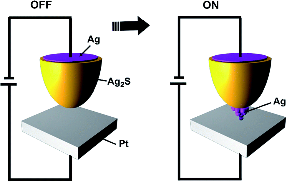 | ||
| Fig. 1 Atomic switch ON! | ||
Manipulation of organic molecules using an ultrafine electronic tool such as an STM tip has been similarly demonstrated. In the example shown in Fig. 2A, applying a negative bias voltage to a C60 molecular film using a scanning tunnelling microscope (STM) tip induces controlled oligomerization to dimer, trimer, tetramer, or pentamer of C60 molecules in a vertical direction.12 The process of vertical oligomerization is reversible and so can be used for information writing and erasing with molecular-level resolution. This technique can be applied for molecular bit operations (i.e. for switching between 0 and 1) and corresponds to a bit density of 190 Tbits in−2. On the other hand, polymerization in a lateral direction by tip-based manipulation leads to spatially defined writing of a molecular-level electrically conducting wires (Fig. 2B).13 This involves polymerization of aligned diacetylene molecules by applying a potential pulse from a closely approached STM tip leading to a conductive polyacetylene chain or wire. This stimuli-based molecular manipulation can be performed at some required location on a two-dimensional substrate. Recently, connection of the polyacetylene conductive wire to a single phthalocyanine molecule was also demonstrated.14 These molecular manipulation processes could be used to realize molecule–molecule connections in the synthesis of electronic circuits composed of molecules. This molecular nanoarchitectonics may become a realistic approach to accomplish true molecular devices.
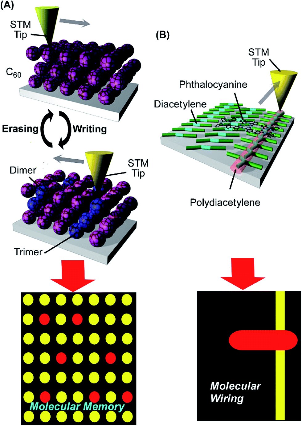 | ||
| Fig. 2 Molecule-based device fabrication: (A) molecular memory; (B) molecular wiring. | ||
Although mechanical action is important for machine operation at the macroscopic scale, mechanical operations involving molecules and development of molecular machines are at a nascent stage. The following two examples depend on quite different mechanical inputs for molecular manipulation. In the first (Fig. 3A), direct pushing of a single pentacene molecule was performed by approaching an STM tip.15 Vertical or lateral manipulation of the STM tip was made without any applied bias voltage. Molecular manipulation, which can be seen as mechanical switching, induces variation in the electronic bonding configuration of the pentacene molecule. In sharp contrast to the abovementioned nanoscopic manipulation, the example illustrated in Fig. 3B uses macroscopic mechanical motions at the tens-of-centimetres scale for control of molecular machines.16 Molecular machines were embedded at the dynamic two-dimensional plane of an air–water interface and then reversibly manipulated between cavity and open forms, resulting in capture and release of aqueous guest molecules. Placing molecular machines in a dynamic interface space of molecular-level thickness and applying force in a defined direction induce concerted conformational changes. As a result, operations across different length scales, in this case with a billion-fold factor of scale (nm to m), can be connected.17 Thus, manual manipulation at the macroscopic level can be used to operate molecular machines. Although molecular-level functions are mainly considered in past designs of molecular machines, connection of molecular machines with our life-scale activities would be accomplished especially by the latter approach.
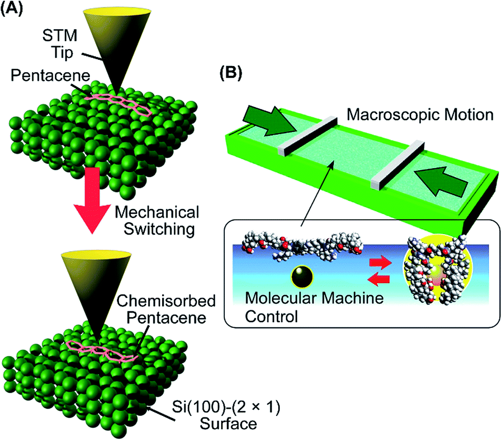 | ||
| Fig. 3 Two extremely different modes for molecular manipulation: (A) with nanotip; (B) macroscopic mechanical motion. | ||
2.2. Materials creation
Materials synthesis involving the agglomeration of two or more existing materials is a powerful strategy for materials creation by nanoarchitectonics as can be seen in the versatile formation of layered structures using appropriate techniques such as Langmuir–Blodgett (LB)18 and layer-by-layer (LbL) assembly.19 Quite different nanocomponents can be assembled into LbL heterostructures to obtain novel functions. For example, alternate layered structures of reduced graphene oxide and an ionic liquid (Fig. 4A) can be prepared by facile adsorption of ionic liquid onto graphene oxide, followed by in situ reduction and polyelectrolyte-assisted LbL assembly.20 This method alleviates the problem of strong graphene stacking and allows the introduction of a fluid interlayer. The materials formed possess nanospaces with a highly π-electron-rich environment, which was used in the fabrication of a sensor system selective for vapours of toxic aromatic compounds in the presence of aliphatic analogues. Spontaneous formation of hetero-stack layered nanoarchitectures from two different nanosheets, transition-metal layered double hydroxide (LDH, cationic) and graphene oxides (anionic), can be performed by simple mixing (Fig. 4B).21 The resulting composites exhibit synergistic effects involving both types of nanosheets. High capacitance (ca. 6 times greater than that of reduced graphene oxide) upon hybridizing with redox-active hydroxide nanosheets was confirmed. Also, alternate layering of conductive graphene and insulating hydroxide nanosheets facilitates charge transfer in the electrochemical process, resulting in good charge and discharge properties at high frequency. These approaches in layered nanoarchitectonics would lead to versatile methods to create materials through a wide choice and combination of building blocks. Advantages of this layered nanoarchitectonics for materials creation are demonstrated in examples shown below.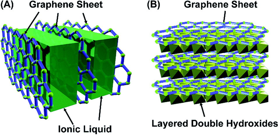 | ||
| Fig. 4 Versatile sandwich nanoarchitectonics: (A) graphene with ionic liquid; (B) graphene with layered double hydroxide. | ||
Materials created using the nanoarchitectonics concept can also exhibit dynamic properties and flexibility. The dynamic nature of materials composed of nanosheets based on materials exchange, diffusion and adsorption at interlayer nanospaces has been observed. For example, isotope exchange experiments revealed that a layered double hydroxide (LDH), a class of hydrotalcite, exhibited ultrafast carbon cycling of atmospheric CO2 under ambient conditions.22 This finding suggests that the active nature of carbon exchanges between lithosphere and atmosphere. An unexpected phenomenon involving interlayer material diffusion was observed manifesting itself as a massive swelling behaviour of stacked nanosheets (43![[thin space (1/6-em)]](https://www.rsc.org/images/entities/char_2009.gif) 000 layers) in water containing amine compounds such as 2-dimethylaminoethanol.23 The swelling behaviour increases the interlayer space ca. 100-fold in one direction to ca. 90 nm while maintaining its three-dimensional lattice architecture. The swollen materials can be regarded as aqua-crystals, and might be applied generally to various layered crystals synthesized using the nanoarchitectonic approach with designed compositions. The concept of control of the excessive interlayer spacing might also be extended to gel materials with giant mechanical anisotropy. For instance, a controlled dispersion of negatively charged titanate nanosheets was forced to align cofacially upon application of a strong magnetic field (Fig. 5).24 Electrostatic repulsion within the cofacial alignment is thus maximized resulting in a quasicrystalline ordering. This ordering leads to mechanical anisotropy, where deformation can be easily induced by applying parallel shear forces but compression is suppressed against an applied orthogonal force. The content of the nanosheets is less than 1% but the substances obtained might find applications as anti-vibration materials for buildings and vehicles. Nanocomponents contained in controlled structures can be used for macroscopic applications, in this excellent demonstration of nanoarchitectonics.
000 layers) in water containing amine compounds such as 2-dimethylaminoethanol.23 The swelling behaviour increases the interlayer space ca. 100-fold in one direction to ca. 90 nm while maintaining its three-dimensional lattice architecture. The swollen materials can be regarded as aqua-crystals, and might be applied generally to various layered crystals synthesized using the nanoarchitectonic approach with designed compositions. The concept of control of the excessive interlayer spacing might also be extended to gel materials with giant mechanical anisotropy. For instance, a controlled dispersion of negatively charged titanate nanosheets was forced to align cofacially upon application of a strong magnetic field (Fig. 5).24 Electrostatic repulsion within the cofacial alignment is thus maximized resulting in a quasicrystalline ordering. This ordering leads to mechanical anisotropy, where deformation can be easily induced by applying parallel shear forces but compression is suppressed against an applied orthogonal force. The content of the nanosheets is less than 1% but the substances obtained might find applications as anti-vibration materials for buildings and vehicles. Nanocomponents contained in controlled structures can be used for macroscopic applications, in this excellent demonstration of nanoarchitectonics.
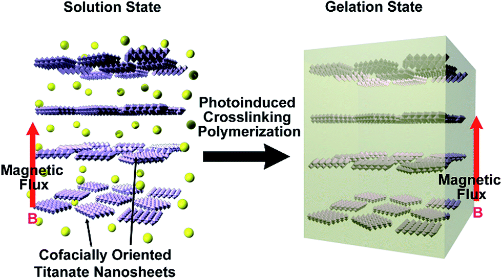 | ||
| Fig. 5 Gel formation with controlled nanosheet architecture. | ||
Unexpected properties of nanoarchitectonic materials have also been observed for the release of materials from layered films of mesoporous capsules contained in hierarchical structures where silica capsules with hierarchical spaces (1000 × 700 × 300 nm central core and 2.2 nm mesopores in their shells) are assembled into a layered structure (Fig. 6).25 Liquid phase materials entrapped at the central cores are released through narrow mesopores with automatic regulation. Release profiles of water and fragrance liquids exhibit stepwise behaviours without external stimuli, i.e., the release operates in periodically ‘automatic’ ON & OFF states. Liquids could be released from the inner central core via the mesoporous channels although liquid supply from the core to the channels is not simple. Only when the channels are almost vacant does liquid move from the interior to the mesoporous channel by capillary penetration involving exchange with external air. Therefore, the rate of liquid release is arrested and then resumes periodically. This system might be applied for stimuli-free controlled drug release or for other innovative medical uses. The prepared system somehow shows an unusual feed-back mechanism that can be a good mimic of biological functions.
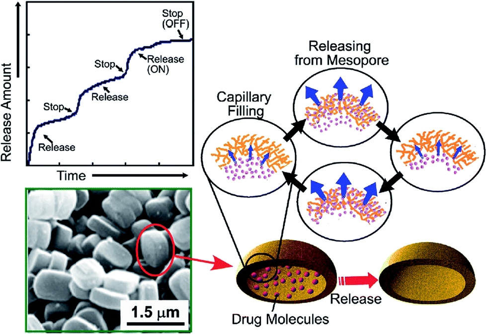 | ||
| Fig. 6 Automatic ON & OFF drug release with images of the used capsules. | ||
2.3. Advanced device materials
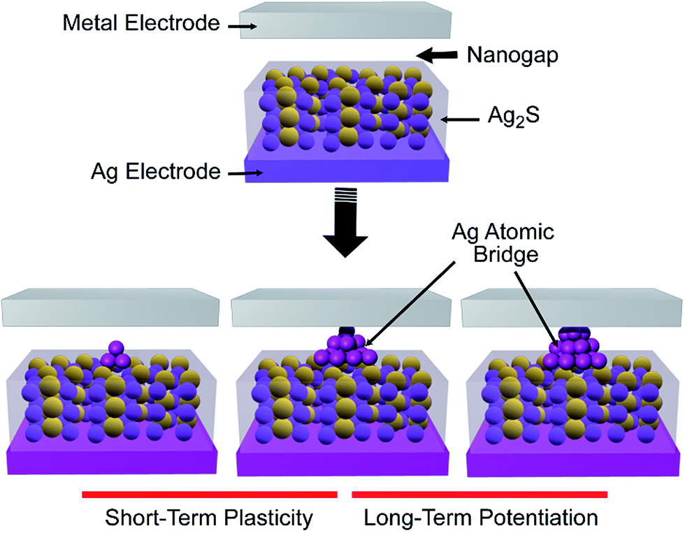
As mentioned above, materials constructed by the nanoarchitectonics concept may exhibit unusual properties where the functionalities of the resulting materials cannot be predicted based on those of the original components. Biological systems are somewhat similar in that biomolecular systems often operate based on cooperative action of assembled components. Various biochemical information conversion and biomolecular systems are prototypical of the nanoarchitectonics concept. In this section, several advanced examples, including bio-inspired systems, are introduced as nanoarchitectonic materials and devices of the future.26The atomic switch described above can be studied as an artificial synapse of short-term plasticity and long-term potentiation as can be observed in some aspects of brain function (Fig. 7).27 The temporal enhancement of conductance upon application of an intermittent input stimulus resulted in memory behaviour with short-term plasticity and a spontaneous decay. Stimulation with higher frequency results in a transition to long-term potentiation. In fact, switching from short-term plasticity to long-term potentiation was demonstrated in a 7 × 7 panel where images of the numerals switched from 1 to 2 depending on the pattern of signal inputs. This synapse-like switching is due only to precipitation of atoms. It is an excellent example demonstrating that high-level functionality can be obtained from atomic-level nanoarchitectonics.
 | ||
| Fig. 7 Artificial synapse with short-term plasticity and long-term potentiation with an atomic switch. | ||
In future, computing systems may become more similar to mammalian brain systems since the performances of such brains for memory and processing operations are apparently superior to those of modern computers. In order to realize this target, networks of atomic switches mimicking brain circuits were fabricated using the nanoarchitectonics concept of self-organization using electroless deposition by pipetting aqueous AgNO3 into a microfluidic apparatus containing Cu seed posts.28 The self-organized silver networks were then functionalized by applying a sulphur melt, resulting in over a billion interconnected atomic-switch inorganic synapses contained in a silver nanowire network. The resulting devices exhibited various performances including weak and strong memristive behaviours and higher harmonic generation. They are potentially useful for developing unconventional computation and investigation models for neuroscientific theories of biological brain function. The use of brain-like functions and mechanisms is surely an attractive way to design computing systems. These nanoarchitectonics approaches based on atomic manipulation and self-organization would realize this dream target.
Efficient power generation is a current and critical problem for sustainable development of society. Ideal self-powered systems might be constructed through the synthesis of appropriate two-dimensional materials in required configurations.29 As illustrated in Fig. 8, a thin film of fluorinated ethylene propylene was located on Al electrodes. At the contacting side of the fluorinated ethylene, propylene, the film was modified by applying an inductively coupled plasma resulting in nanorod structures for improved triboelectric charge density. Sliding the triboelectric layer between two Al electrode stations generates an alternating current and leads to highly efficient energy conversion using mechanical motions. This power-generation system can also be connected with various sensing systems.30 For such device fabrication, regulation of atomic-level structures is also critical as has been recently demonstrated for two-dimensional MoS2. Thin MoS2 flakes generate an oscillating piezoelectric voltage when they are of an odd number of atomic layers, but not when of an even number of layers.31 This implies that detailed nanosized architectonics can be used to control macroscopic devices. This interesting approach may open up ways for usage of energy for our life activities through nano-level materials nanoarchitectonics.
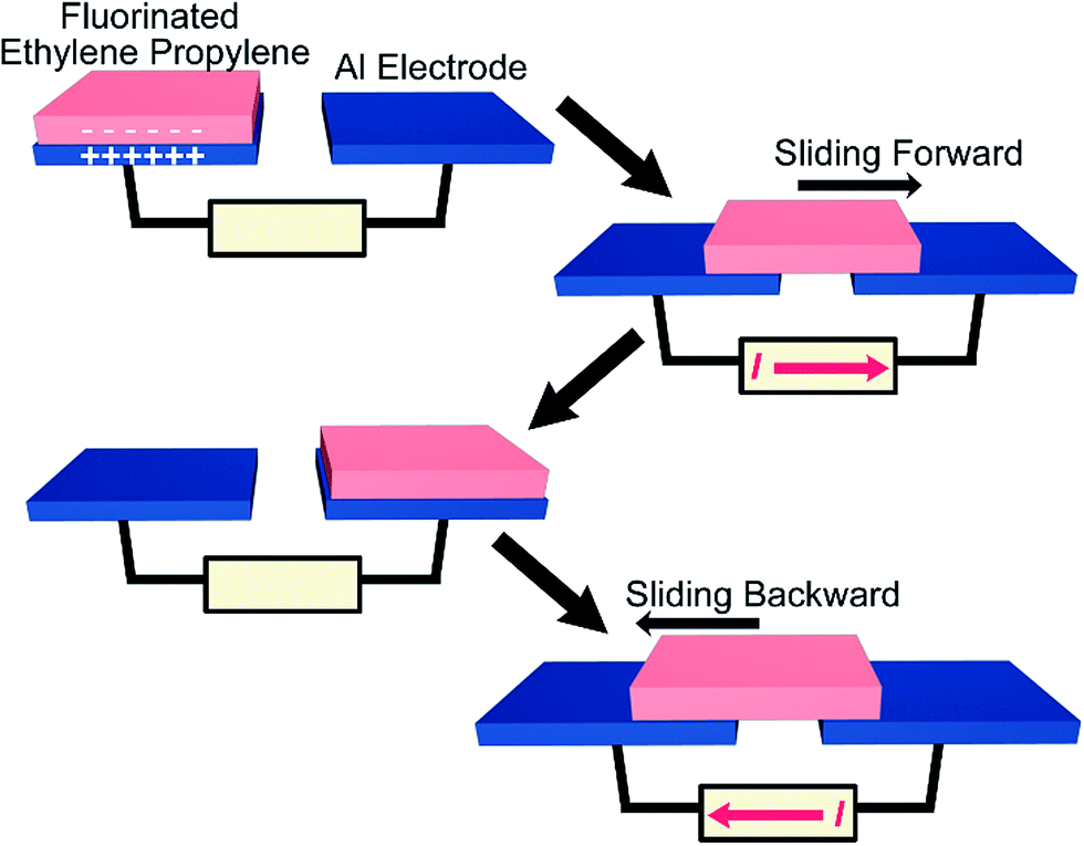 | ||
| Fig. 8 Energy generation based on materials architecture. | ||
3. Future nanoarchitectonics
In this short review, we have introduced a new concept, nanoarchitectonics, as what is appearing on the nanomaterials horizon. This concept represents a total methodology for the construction of functional materials and systems from nano-sized units, from which unusual properties or unexpected functionality might be illicited based on uncertainty or local fluctuations. The nanoarchitectonic concept itself did not suddenly appear but rather has been introduced as a more gradual paradigm shift. Therefore, current (and future) knowledge on nanotechnology can certainly be applied in the development of nanoarchitectonics, and its rapid progress is highly anticipated. Future images of nanoarchitectonics would be flexible and may not tightly fix here.32One distinct difference between nanotechnology and nanoarchitectonics can be found in relation to biosciences. Certain features of nanoarchitectonics including self-organization, mutual effects of multiple components and the unavoidable effects of thermal/statistic fluctuations are also common characteristics of biochemical systems. Many functional biological systems possess ‘soft’ flexible architectures based on the self-organization of functional nano-units (biomolecules) and these in turn operate effectively even in the presence of (or in some cases, because of) thermal fluctuations. Biosystems can be regarded as the ultimate prototype of nanoarchitectonics. Considering this, nanoarchitectonics is expected to provide opportunities for fusion of artificial nanotechnological systems with biosystems. Nanoarchitectonics will approach more closely biochemical systems in contrast to current nanotechnology, which has more in common with hard materials science. For example, self-propelling nanorobots have been recently proposed as nice mimics of living organisms.33 We anticipate that nanoarchitectonics will yield application opportunities in the biological and pharmaceutical sciences providing useful nanomaterials to benefit our day-to-day lives.
Acknowledgements
This work was partly supported by World Premier International Research Center Initiative (WPI Initiative), MEXT, Japan.Notes and references
- T. Stephenson, Z. Li, B. Olsen and D. Mitlin, Energy Environ. Sci., 2014, 7, 209 Search PubMed
; D. W. Wang and D. Su, Energy Environ. Sci., 2014, 7, 576 Search PubMed
- A. J. Heegar, Adv. Mater., 2014, 26, 10 CrossRef CAS PubMed
- M. Aono, Sci. Technol. Adv. Mater., 2011, 12, 040301 CrossRef CAS
- M. Magoga and C. Joachim, Phys. Rev. B: Condens. Matter Mater. Phys., 1999, 59, 16011 CrossRef CAS
- S. Hecht, Angew. Chem., Int. Ed., 2003, 42, 24 CrossRef CAS
- P. S. Weiss, ACS Nano, 2007, 1, 379 CrossRef CAS PubMed
- X. Q. Chen, P. Li, H. Tong, T. Kako and J. H. Ye, Sci. Technol. Adv. Mater., 2011, 12, 044604 CrossRef CAS
- L. K. Shrestha, Q. Ji, T. Mori, K. Miyazawa, Y. Yamauchi, J. P. Hill and K. Ariga, Chem.–Asian J., 2013, 8, 1662 CrossRef CAS PubMed
- K. Ariga, S. Ishihara, H. Abe, M. Li and J. P. Hill, J. Mater. Chem., 2012, 22, 2369 RSC
- K. Ariga, Q. Ji, M. J. McShane, Y. M. Lvov, A. Vinu and J. P. Hill, Chem. Mater., 2012, 24, 728 CrossRef CAS
- T. Hasegawa, K. Terabe, T. Tsuruoka and M. Aono, Adv. Mater., 2012, 24, 252 CrossRef CAS PubMed
- M. Nakaya, M. Aono and T. Nakayama, ACS Nano, 2011, 5, 7830 CrossRef CAS PubMed
- M. Nakaya, S. Tsukamoto, Y. Kuwahara, M. Aono and T. Nakayama, Adv. Mater., 2010, 22, 1622 CrossRef CAS PubMed
- Y. Okawa, S. K. Mandal, C. Hu, Y. Tateyama, S. Goedecker, S. Tsukamoto, T. Hasegawa, J. K. Gimzewski and M. Aono, J. Am. Chem. Soc., 2011, 133, 8227 CrossRef CAS PubMed
- O. A. Neucheva, F. Ample and C. Joachim, J. Phys. Chem. C, 2013, 117, 26040 CAS
- K. Ariga, T. Mori and J. P. Hill, Adv. Mater., 2012, 24, 158 CrossRef CAS PubMed
- K. Ariga, T. Mori, S. Ishihara, K. Kawakami and J. P. Hill, Chem. Mater., 2014, 26, 519 CrossRef CAS
- K. Ariga, Y. Yamauchi, T. Mori and J. P. Hill, Adv. Mater., 2013, 25, 6477 CrossRef CAS PubMed
- G. Decher, Science, 1997, 277, 1232 CrossRef CAS
- Q. Ji, I. Honma, S.-M. Paek, M. Akada, J. P. Hill, A. Vinu and K. Ariga, Angew. Chem., Int. Ed., 2010, 49, 9737 CrossRef CAS PubMed
- R. Ma, X. Liu, J. Liang, Y. Bando and T. Sasaki, Adv. Mater., 2014, 26, 4173 CrossRef CAS PubMed
- S. Ishihara, P. Sahoo, K. Deguchi, S. Ohki, M. Tansho, T. Shimizu, J. Labuta, J. P. Hill, K. Ariga, K. Watanabe, Y. Yamauchi, S. Suehara and N. Iyi, J. Am. Chem. Soc., 2013, 135, 18040 CrossRef CAS PubMed
- F. Geng, R. Ma, A. Nakamura, K. Akatsuka, Y. Ebina, Y. Yamauchi, N. Miyamoto, Y. Tateyama and T. Sasaki, Nat. Commun., 2013, 4, 1632 CrossRef PubMed
- M. Liu, Y. Ishida, Y. Ebina, T. Sasaki, T. Hikima, M. Takata and T. Aida, Nature, 2015, 517, 68 CrossRef CAS PubMed
- Q. Ji, M. Miyahara, J. P. Hill, S. Acharya, A. Vinu, S. B. Yoon, J.-S. Yu, K. Sakamoto and K. Ariga, J. Am. Chem. Soc., 2008, 130, 2376 CrossRef CAS PubMed
- K. Ariga, K. Kawakami, M. Ebara, Y. Kotsuchibashi, Q. Ji and J. P. Hill, New J. Chem., 2014, 38, 5149 RSC
- T. Ohno, T. Hasegawa, T. Tsuruoka, K. Terabe, J. K. Gimzewski and M. Aono, Nat. Mater., 2011, 10, 591 CrossRef CAS PubMed
- A. V. Avizienis, H. O. Sillin, C. Martin-Olmos, H. H. Shieh, M. Aono, A. Z. Stieg and J. K. Gimzewski, PLoS One, 2012, 7, e42772 CAS
- S. Wang, Y. Xie, S. Niu, L. Lin and Z. L. Wang, Adv. Mater., 2014, 26, 2818 CrossRef CAS PubMed
- H. Zhang, Y. Yang, Y. Su, J. Chen, C. Hu, Z. Wu, Y. Liu, C. P. Wong, Y. Bando and Z. L. Wang, Nano Energy, 2013, 2, 693 CrossRef CAS PubMed
- W. Wu, L. Wang, Y. Li, F. Zhang, L. Lin, S. Niu, D. Chenet, X. Zhang, Y. Hao, T. F. Heinz, J. Hone and Z. L. Wang, Nature, 2014, 514, 470 CrossRef CAS PubMed
- For example, for activities on nanoarchitectonics, see: http://www.nims.go.jp/mana/research/index.html; http://www.nims.go.jp/mana/research/highlights/index.html.
- G. Zhao and M. Pumera, Langmuir, 2013, 29, 7411 CrossRef CAS PubMed
| This journal is © The Royal Society of Chemistry 2015 |