
Advancements in all-solid-state hybrid solar cells based on organometal halide perovskites
Shaowei
Shi
ab,
Yongfang
Li
c,
Xiaoyu
Li
*ab and
Haiqiao
Wang
*ab
aState Key Laboratory of Organic–Inorganic Composites, Beijing University of Chemical Technology, Beijing 100029, China. E-mail: wanghaiqiao@mail.buct.edu.cn; lixy@mail.buct.edu.cn
bBeijing Engineering Research Center for the Synthesis and Applications of Waterborne Polymers, Beijing University of Chemical Technology, Beijing 100029, China
cCAS Key Laboratory of Organic Solids, Institute of Chemistry, Chinese Academy of Sciences, Beijing 100190, China
First published on 8th January 2015
Abstract
Over the past several years, organic–inorganic hybrid perovskites have gained considerable research attention due to their direct band gap, large absorption coefficient, ambipolar diffusion and long carrier diffusion length, and have revolutionized the prospects of emerging photovoltaic technologies, with the highest power conversion efficiency of over 19% achieved under laboratory conditions. In this perspective, we summarize the recent developments in perovskite solar cells (from April 2009 to December 2014), describe the unique properties of organometal halide perovskites leading to their rapid emergence, and discuss challenges such as stability and environmental issues to be faced in the future.
 Shaowei Shi | Shaowei Shi received a BS degree at Beijing University of Chemical Technology in 2010. Now he is a Ph.D. student in Prof. Haiqiao Wang's group, at the State Key Laboratory of Organic–Inorganic Composites, Beijing University of Chemical Technology. His research interests include the synthesis of organic semiconducting materials, and their application in electronic devices. |
 Yongfang Li | Dr Yongfang Li has been a professor in the Institute of Chemistry, Chinese Academy of Sciences (ICCAS) since 1993, a professor in the College of Chemistry, Chemical Engineering and Materials Science, Soochow University since 2012, and a Member of the Chinese Academy of Sciences since 2013. He obtained his M.Sc. in Chemistry from Eastern China University of Science and Technology in 1982, and his Ph.D. in physical chemistry from Fudan University in 1986. His major research areas include electrochemistry of conducting polymers, and photovoltaic materials and devices for polymer solar cells. He has published more than 490 papers, and the published papers have been cited by others more than 15 |
 Xiaoyu Li | Prof. Xiaoyu Li received his B.S. in the Chemistry Department, Shandong University (1981), his M.Sc. in the Department of Polymer Science, Beijing University of Chemical Technology (1985), and his Ph.D. in the College of Materials Science and Engineering, Beijing University of Chemical Technology (1998). He is currently a Professor of the State Key Laboratory of Organic–Inorganic Composites, Head of Department of Organic Functional Materials, Beijing University of Chemical Technology. His research areas involve emulsion polymerization theory, synthesis and application of water-based paint, adhesive and ink materials, and new types of photoelectric functional materials. |
 Haiqiao Wang | Prof. Haiqiao Wang received his B.S. (1983), and M.Sc. (1989) in the Department of Chemistry, Huazhong University of Science and Technology, and his Ph.D. (1998) in the Department of Photoelectric Engineering, Huazhong University of Science and Technology. After postdoctoral work at Tsinghua University (1999–2001), he joined Beijing University of Chemical Technology. He is currently a Professor of the State Key Laboratory of Organic–Inorganic Composites, Beijing University of Chemical Technology. His research areas involve materials and devices of organic light emitting diodes, polymer solar cells and organic field-effect transistors, and synthesis and application of water-based polymers. |
1. Introduction
Increasing energy demands and concerns about global warming drive the exploration/development of clean, inexpensive and renewable energy sources. Several new energy technologies for converting solar energy into electricity, including organic photovoltaic cells (OPVs), dye sensitized solar cells (DSSCs) and quantum dot solar cells (QDSCs), have attracted significant attention as low-cost alternatives to conventional silicon-based solar cells. Recently, hybrid organometal halide perovskites, which were initially employed in DSSCs as light absorbers, have gradually become one of the most important active materials for all-solid-state solar cells (which can be named as perovskite solar cells) due to their direct band gap, large absorption coefficient, ambipolar diffusion and long carrier diffusion length, with the highest efficiency of up to ∼20%. Two important journals, Science1 and Nature,2 both highlighted perovskite photovoltaics as one of the biggest breakthroughs of the year 2013.3“Perovskite”, which is named after the Russian mineralogist, L. A. Perovski (1792–1856), is defined as one class of compounds which crystallise in the ABX3 structure (e.g. CaTiO3).4 An ideal perovskite structure has a cubic Pm![[3 with combining macron]](https://www.rsc.org/images/entities/char_0033_0304.gif) m crystal structure, which consists of a three-dimensional (3-D) framework of corner-sharing BX6 octahedron with the A ion placed in the cuboctahedral interstices, as shown in Fig. 1. In the case of organometal trihalide perovskites, A is an organic cation (typically CH3NH3+ or HN
m crystal structure, which consists of a three-dimensional (3-D) framework of corner-sharing BX6 octahedron with the A ion placed in the cuboctahedral interstices, as shown in Fig. 1. In the case of organometal trihalide perovskites, A is an organic cation (typically CH3NH3+ or HN![[double bond, length as m-dash]](https://www.rsc.org/images/entities/char_e001.gif) CHNH3+), B is a metal cation (typically Sn2+ or Pb2+), and X is a halide anion (typically Cl−, Br− or I−). Goldschmidt's tolerance factor (t), t = (RA + RX)/[21/2(RB + RX)], (where RA, RB and RX are the ionic radii for the ions in the A, B and X sites, respectively; t = 1 corresponds to a perfectly packed perovskite structure) and octahedral factor (μ), μ = RB/RX, can be used to estimate the stability and distortion of the perovskite structure.5–7
CHNH3+), B is a metal cation (typically Sn2+ or Pb2+), and X is a halide anion (typically Cl−, Br− or I−). Goldschmidt's tolerance factor (t), t = (RA + RX)/[21/2(RB + RX)], (where RA, RB and RX are the ionic radii for the ions in the A, B and X sites, respectively; t = 1 corresponds to a perfectly packed perovskite structure) and octahedral factor (μ), μ = RB/RX, can be used to estimate the stability and distortion of the perovskite structure.5–7
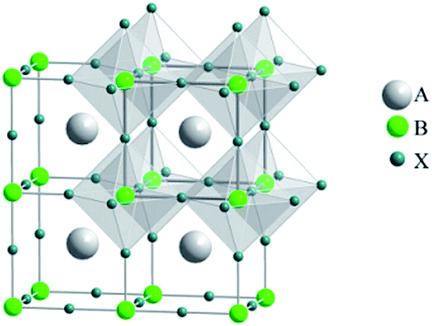 | ||
| Fig. 1 The basic perovskite structure (ABX3). Reprinted with permission.7 | ||
In the present paper, we aim to offer a brief review on the application of hybrid organic–inorganic perovskites (typically methylammonium lead halide perovskite) in different photovoltaic devices, including the mesoporous metal oxide solar cell, meso-superstructured solar cell and planar heterojunction solar cell. Although great progress has been achieved in the past three years, continued development of perovskite solar cells will require a better understanding of the relationships between the perovskite structure, device architecture, hole–electron conductor, and device performance than is currently available.
2. Progress in hybrid organic–inorganic perovskite solar cells
Since O'Regan and Grätzel first introduced the concept of DSSCs in 1991,8 in the following two decades, DSSCs have drawn great attention both in scientific and technological aspects and are considered to be a potential alternative to conventional inorganic silicon-based solar cells due to the low processing costs and inexpensive constituent materials. Generally, a DSSC contains a transparent conducting oxide electrode (typically fluorine-doped tin oxide (FTO) or indium-doped tin oxide (ITO)), a dye-sensitized mesoporous semiconductor metal oxide (typically nanocrystalline TiO2) film, a platinum (Pt) counter electrode, and an electrolyte containing redox couples (typically I−/I3−) dissolved in a solvent. However, although power conversion efficiencies (PCEs) of close to 13% have been achieved with this device architecture,9 such cells suffer from potential leakage problems associated with the corrosive and volatile nature of the liquid electrolyte and, thus, may be impractical for large-scale applications. In 1998, the first example of solid-state dye-sensitized solar cells (ss-DSSCs) emerged by using a solid hole-transporting material (HTM) 2,2′,7,7′-tetrakis(N,N-di-p-methoxyphenylamine)-9,9′-spirobifluorene (spiro-OMeTAD or spiro) instead of the conventional liquid redox electrolyte.10 With this change, ss-DSSCs appeared to be quickly becoming both efficient and stable. Nevertheless, in the following long period of time, this type of cell did not reach the predetermined level of high efficiencies, yielding a maximum PCE of 7.2% based on tris(2-(1H-pyrazol-1-yl)pyridine)cobalt(III) doped spiro-OMeTAD and an organic photosensitizer with a high molar extinction coefficient.11The real breakthrough in ss-DSSCs came in 2012, when Grätzel et al.12 and Snaith et al.13 independently employed CH3NH3PbI3 (MAPbI3) and CH3NH3PbI2Cl (MAPbI2Cl) perovskite nanocrystals as light harvesters using submicron thick mesoporous TiO2 film and spiro-MeOTAD as an electron- and a hole-transporting layer. PCEs of 9.7% and 7.6% were achieved under AM1.5G illumination along with excellent long term stability. Moreover, by replacing the n-type mesoporous TiO2 with insulating mesoporous Al2O3, evolution of the ss-DSSC, which is termed as the meso-superstructured solar cell (MSSC) was developed by Snaith et al.13 The FTO/blocking layer (bl)-TiO2/mesoporous (mp)-Al2O3/MAPbI2Cl/spiro-OMeTAD/Ag-based device showed a PCE of 10.9%.13 Etgar and coworkers also fabricated a hole conductor-free MAPbI3/mp-TiO2 heterojunction solar cell (FTO/bl-TiO2/mp-TiO2/MAPbI3/Au) and achieved a PCE of 5.5%.14 All the above mentioned studies proved that this organometal halide perovskite can not only act as an absorber (dye) but also as an ambipolar charge transporter, indicating the possibility for applying in various device architectures.
Actually, early in 2009, organometal halide perovskites MAPbBr3 and MAPbI3 were initially attempted in conventional liquid electrolyte-based DSSCs, yielding PCEs of 3.13% and 3.81%, respectively (see Fig. 2).15 Later, in 2011, via optimization of the titania surface and perovskite (MAPbI3) processing, Park and coworkers further improved the PCE to 6.54% in a perovskite quantum dot-sensitized 3.6 μm thick TiO2 film under AM1.5G 1 sun illumination.16 The authors also reported a (CH3CH2NH3)PbI3-sensitized solar cell with an iodide-based redox electrolyte and achieved a PCE of 2.4%.17 This pioneering work opened the prelude to organometal halide perovskites to be applied as active layers in ss-DSSCs. However, electrolyte-based devices were usually unstable and the performance degraded rapidly due to the dissolution or decomposition of the perovskite in the liquid electrolyte.
 | ||
| Fig. 2 (a) The schematic of perovskite-sensitized TiO2 undergoing photoexcitation and electron transfer. (b) The incident photon-to-electron conversion efficiency (IPCE) spectra for MAPbBr3/MAPbI3-sensitized solar cells. Reprinted with permission.15 | ||
 | ||
| Fig. 3 Solution-based deposition methods (e.g. MAPbI3). (a) One step precursor deposition (OSPD). Reprinted with permission.53 (b) Sequential deposition process (SDP). Reprinted with permission.54 (c) Two step spin-coating deposition (TSSD). Reprinted with permission.21 | ||
After the breakthrough work of ss-DSSCs based on organometal halide perovskites,12,13 in 2013, two papers published in the journal Nature lifted the study of perovskite solar cells to a new level.18,19 First, by using a sequential deposition process to fabricate MAPbI3 films, a remarkable PCE of 15% was measured in a FTO/bl-TiO2/mp-TiO2/MAPbI3/spiro-OMeTAD/Au-based device.18 Subsequently, Snaith and coworkers deposited a high-quality MAPbI3−xClx film via dual source vacuum deposition in a planar heterojunction (PHJ) perovskite solar cell (FTO/bl-TiO2/MAPbI3−xClx/spiro-OMeTAD/Ag) and achieved a PCE of 15.4%.19 Seok and coworkers also obtained a PCE of 12% in a FTO/bl-TiO2/mp-TiO2/MAPbI3/PTAA/Au-based device by replacing the conventional spiro-OMeTAD HTM with poly(triarylamine) (PTAA).20 Since then, follow-up work such as the morphology and crystal optimization, HTM/ETM (electron-transporting material) adjustment and interface/band-gap engineering further improved the device performance to nearly 20% efficiency, opening up a new direction for developing highly efficient solar cells with a low cost and good stability.
At present, two types of perovskite solar cells, based on a porous or planar architecture, are the focus of research. It is worth pointing out that in a porous device, mesoporous “scaffolds” can not only act as conductors (e.g. TiO2, ZnO, NiO) but also as insulators (e.g. Al2O3, ZrO2, SiO2). For the purpose of distinguishing these two types of devices, herein, we classify this porous device into two groups, including mesoporous metal oxide perovskite solar cell (MMOPSC) (with mesoporous conductors) and the above-mentioned MSSC (with mesoporous insulators). So far the highest PCEs achieved from MMOPSC, MSSC and planar heterojunction perovskite solar cell (PHJPSC) are 17.01%,21 15.9% (ref. 22) and 19.3%,23 respectively.
3. Deposition processes for perovskite films
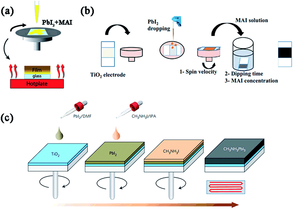
As the core part of perovskite solar cells, the morphology and crystal structure of perovskite absorbers are important for achieving high-performance devices. So far seven main deposition methods have been reported including one step precursor deposition (OSPD), sequential deposition process (SDP), two step spin-coating deposition (TSSD), dual source vacuum deposition (DSVD), sequential vapour deposition (SVD), vapour-assisted solution process (VASP) and spray-coating deposition (SCD). Among the above mentioned methods, devices fabricated using OSPD, SDP, TSSD, DSVD or SVD have yielded PCEs of over 15%, while PCEs of over 10% have been achieved using VASP or SCD (Table 1).3.1 Solution-based deposition methods (OSPD, SDP, TSSD, SCD) (Fig. 3)
The initial report of one step precursor deposition for organo-lead halide perovskite solar cells was from Miyasaka and coworkers in 2009, which involved spin-coating a precursor solution containing MAX and PbX2 (X = Br, I) on the mp-TiO2 layer to form nanocrystalline MAPbBr3 or MAPbI3.15 For the widely studied MAPbI3 or MAPbI3−xClx-based perovskite solar cells, γ-butyrolactone (GBL) and N,N-dimethylformamide (DMF) are commonly used solvents for dissolving PbX2 (X = I, Cl) and MAI, in which the mole ratio of MAI and PbI2 is 1![[thin space (1/6-em)]](https://www.rsc.org/images/entities/char_2009.gif) :1 while the MAI and PbCl2 are present in a molar ratio of 3:1. Generally, the perovskite precursor solution (∼40 wt%) is firstly stirred at a certain temperature (e.g. 80 °C) overnight before spin-coating on the substrate. Then thermal annealing (∼100 °C) is performed to remove the solvent and complete the transformation of the precursor to the resulting crystalline perovskite. The thickness of the perovskite film is tuned by changing the precursor concentration and/or spin speed of the perovskite precursor solution. The problem in this deposition method is the uncontrolled crystallization process of the perovskite, which always results in a wide spread of photovoltaic performance and low reproducibility in the resulting devices (especially for porous structure-based devices). To avoid the large perovskite grains and uncovered pin-hole areas, follow-up morphology optimizations such as solvent-engineering technology (e.g. using a mixed solvent or fast crystallization–deposition),24–30 thermal annealing,31–34 and additive treatment (e.g. 1,8-diiodooctane (DIO), NH4Cl and MACl)35–38 have been reported by several groups and excellent efficiencies have been achieved. To date, OSPD is still considered as one of the simplest and most important deposition methods, and the record efficiency (19.3%) of perovskite solar cells was achieved via this approach.23
:1 while the MAI and PbCl2 are present in a molar ratio of 3:1. Generally, the perovskite precursor solution (∼40 wt%) is firstly stirred at a certain temperature (e.g. 80 °C) overnight before spin-coating on the substrate. Then thermal annealing (∼100 °C) is performed to remove the solvent and complete the transformation of the precursor to the resulting crystalline perovskite. The thickness of the perovskite film is tuned by changing the precursor concentration and/or spin speed of the perovskite precursor solution. The problem in this deposition method is the uncontrolled crystallization process of the perovskite, which always results in a wide spread of photovoltaic performance and low reproducibility in the resulting devices (especially for porous structure-based devices). To avoid the large perovskite grains and uncovered pin-hole areas, follow-up morphology optimizations such as solvent-engineering technology (e.g. using a mixed solvent or fast crystallization–deposition),24–30 thermal annealing,31–34 and additive treatment (e.g. 1,8-diiodooctane (DIO), NH4Cl and MACl)35–38 have been reported by several groups and excellent efficiencies have been achieved. To date, OSPD is still considered as one of the simplest and most important deposition methods, and the record efficiency (19.3%) of perovskite solar cells was achieved via this approach.23
Another important solution-based deposition is the sequential deposition process, which was originally introduced by Mitzi et al. in 1998,39 then employed in perovskite solar cells by Grätzel et al. in 2013.18 In this process, a PbX2 (X = I, Cl40) solution in DMF (or dimethylsulphoxide (DMSO)41) is first spin-coated (one or more times42) on the top of porous or planar substrates, followed by dipping it into a solution of MAI in 2-propanol (seconds to tens of minutes) to transform into the perovskite. The perovskite crystal size and orientation on the substrate can be controlled by modifying the prewetting time of 2-propanol or reaction temperature in the second step.43–45 So far, using this deposition, perovskite solar cells based on mesoporous metal oxide, meso-superstructured or planar structures have achieved the highest PCE of 15%,18 10.8% (ref. 46) and 15.7%,47 respectively. Compared with OSPD, SDP is more beneficial to improve the coverage, pore-filling, and morphology of the deposited perovskite in porous substrates, thereby further improving the device performance. However, for most PHJ perovskite solar cells, SDP cannot perform as successfully as in nanostructured devices. Without the porous “scaffold”, it is hard for MAI to penetrate into the PbX2 films due to the limited reaction interface area, leading to a long reaction time and/or low conversion rate of PbX2.48 Also, large randomly distributed grains always appear during the quick crystallization of perovskite, which results in a very rough perovskite film and low efficiency.49
In 2014, Huang and coworkers reported an efficient planar perovskite solar cell (PCE = 15.4%) using a two step spin-coating deposition method,49 in which the solution of PbI2 in DMF and the solution of MAI in 2-propanol were spin-coated step by step on the ITO/PEDOT:PSS-based substrate at first, followed by thermal annealing at 100 °C to drive the interdiffusion of precursors (this step can be skipped via controlling well the thickness of PbI2 and the process of adding MAI50). Later, Park et al. found that the size of the MAPbI3 cuboids was very strongly dependent on MAI concentration and the exposure time of PbI2 to the MAI solution before spin coating, and high PCE of 17.01% was achieved using this modified TSSD.21,51 Lidzey et al. explored the use of ultra-sonic spray-coating as a deposition technique to create MAPbI3−xClx perovskite thin-films in ambient conditions.52 Precursor solution of MAI and PbCl2 (3:1 molar ratio) in DMF or DMSO was deposited on the substrates from a single pass of the spray-head, then transformed into MAPbI3−xClx through thermal annealing. A planar device with an ITO/PEDOT:PSS/MAPbI3−xClx/[6,6]-phenyl C61-butyric acid methyl ester (PC60BM)/Ca/Al structure yielded a PCE of 11.1% with an average efficiency of 7.8%, which was comparable to the devices fabricated via spin-coating, showing the commercial potential of SCD used in the large-area, low-cost, efficient manufacture of perovskite solar cells.
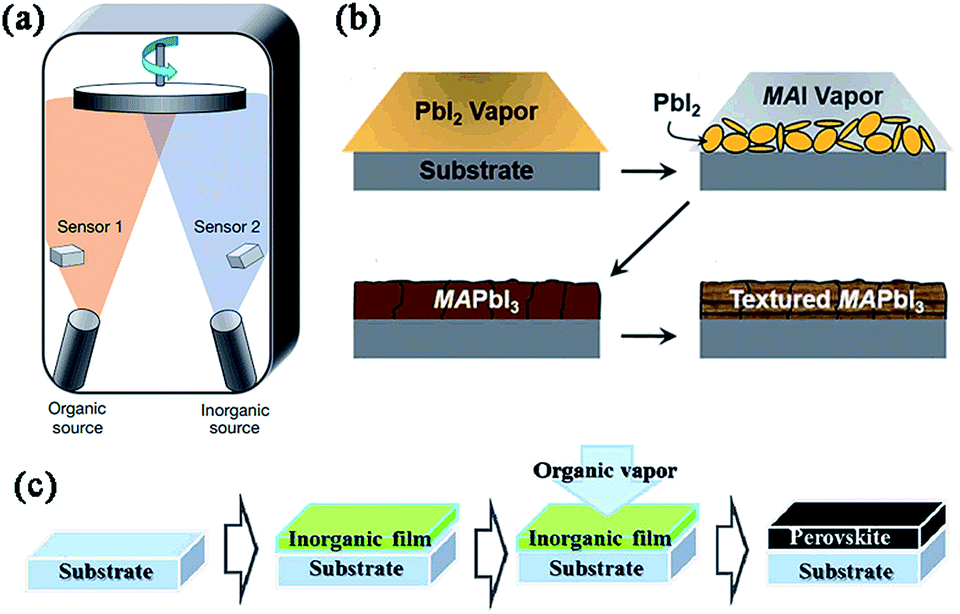
3.2 Vapor-based deposition methods (DSVD, SVD, VASP) (Fig. 4)
Vapor-based deposition processes are not used as commonly as solution-based deposition processes (especially OSPD and SDP), mainly due to the increasing manufacturing cost. In 2013, Snaith and coworkers initially fabricated a MAPbI3−xClx-based PHJ perovskite solar cell (FTO/bl-TiO2/MAPbI3−xClx/spiro-OMeTAD/Ag) via dual source vacuum deposition and achieved a high PCE of 15.4%.19 In this process, MAI and PbCl2 were evaporated simultaneously from separate sources and a superior uniformity of the perovskite films was observed over a range of length scales. Subsequently, using DSVD, Bolink and Sarkar groups reported three types of PHJ devices based on ITO/PEDOT:PSS/poly-TPD/MAPbI3/PC60BM/Au, FTO/NiO/MAPbI3−xClx/PC60BM/Ag and FTO/CuSCN/MAPbI3−xClx/PC60BM/Ag, yielding PCEs of 14.8%, 7.26%, and 3.8%, respectively.In 2014, Cui55 and Lin56et al. developed a sequential vapor deposition process, in which PbX2 (X = I, Cl) and MAI were vapour-deposited on the substrates layer by layer. PbX2 reacts with MAI in situ, followed by thermal annealing to complete the perovskite crystal transformation. This deposition process is very similar to the above mentioned precursor interdiffusion deposition method (TSSD), except that SVD uses vapor deposition. Compared with the perovskite films fabricated via DSVD, SVD fabricated films demonstrate a larger crystal domain size, which is beneficial in improving transport properties of carriers. Also, SVD enhances the control on the perovskite morphology by independent manipulation of PbX2 and MAI. Using SVD, Cui and coworkers prepared a uniform, smooth MAPbI3 film and fabricated an easy planar perovskite solar cell consisting of only a MAPbI3/fullerene (C60) layer sandwiched between two electrical contacts.55 No hole conductor (e.g. PEDOT:PSS or NiOx) was needed in this system and a PCE of 5.4% was achieved under AM1.5G one sun illumination. Lin et al. also achieved a high PCE of 15.4% in an ITO/PEDOT:PSS/MAPbI3−xClx/C60/bathophenanthroline (Bphen)/Ca/Ag-based device.56
Yang and coworkers reported a blended deposition method called vapour-assisted solution process to fabricate MAPbI3 films.48 First, the solution of PbI2 in DMF was spin-coated on the FTO/bl-TiO2 substrates, and dried at 110 °C for 15 min. Then the PbI2-coated substrates were annealed in MAI vapor at 150 °C in a N2 atmosphere for the desired time to yield the perovskite films. After cooling down, the as-prepared substrates were washed with isopropanol, dried and annealed to complete the deposition. The perovskite film derived from this approach exhibited full surface coverage, uniform grain structure with grain size up to micrometers, and ∼100% precursor transformation completeness. The PHJ device based on FTO/bl-TiO2/MAPbI3−xClx/spiro-OMeTAD/Ag yielded a PCE of 12.1%. Later, via VASP, the authors introduced a controllable self-induced passivation technique by tuning the amount of PbI2 species in perovskite grain boundaries and at the relevant interfaces, which was helpful for understanding the carrier behavior along the heterojunctions and the polycrystalline nature of hybrid perovskite thin films.57–59
| Deposition process (DP) | Device structure | J sc (mA cm−2) | V oc (V) | FF (%) | PCE (%) | Ref. |
|---|---|---|---|---|---|---|
| OSPD | ITO/PEIE/bl-TiO2(Y)/MAPbI3−xClx/spiro/Au | 22.75 | 1.13 | 75.01 | 19.3 | 23 |
| SDP | ITO/bl-ZnO/MAPbI3/spiro/Ag | 20.4 | 1.03 | 74.9 | 15.7 | 47 |
| TSSD | ITO/bl-TiO2/mp-TiO2/MAPbI3/spiro/Au | 21.64 | 1.056 | 74.1 | 17.01 | 21 |
| DSVD | FTO/bl-TiO2/MAPbI3−xClx/spiro/Ag | 21.5 | 1.07 | 67 | 15.4 | 19 |
| SVD | ITO/PEDOT:PSS/MAPbI3−xClx/C60/Bphen/Ca/Ag | 20.9 | 1.02 | 72.2 | 15.4 | 56 |
| VASP | FTO/bl-TiO2/MAPbI3−xClx/spiro/Ag | 19.8 | 0.924 | 66.3 | 12.1 | 48 |
| SCD | ITO/PEDOT:PSS/MAPbI3−xClx/PC60BM/Ca/Al | 16.8 | 0.92 | 72 | 11.1 | 52 |
4. Device architectures of perovskite solar cells
4.1 Mesoporous metal oxide-based perovskite solar cells
At present, tremendous attention has been paid on the optimization of this mesoporous TiO2-based device, including the modification of the TiO2 nanostructure, perovskite layer and HTM, along with the in-depth understanding on the detailed mechanism behind this high efficiency device architecture.73–77 So far, anatase TiO2 nanoparticles are the most frequently and successfully used nanostructures to construct mesoscopic perovskite solar cells, with the highest PCE of over 17%. In 2014, Park and coworkers used rutile TiO2 nanoparticles to fabricate a FTO/bl-TiO2/mp-TiO2(rutile)/MAPbI3/spiro-MeOTAD/Au device.78 Compared to the anatase TiO2-based device, higher electron diffusion coefficients and lower electron recombination were observed in the rutile TiO2-based device, suggesting that more electrons were injected from the perovskite to the rutile TiO2 layer. As a result, although a relatively lower open-circuit voltage (Voc) was observed due to the lower Fermi energy level at equilibrium between TiO2 and perovskite in the rutile-based device, the optimal device demonstrated a PCE of 14.46%, with a short-circuit current density (Jsc) of 20.02 mA cm−2, a Voc of 1.022 V, and a fill factor (FF) of 0.71 at AM1.5G one sun illumination.
Besides the mostly used TiO2 nanoparticles, many other nanostructured TiO2 materials, such as nanosheets,14,79,80 nanorods,81–85 nanotubes,86 nanofibers/nanowires87–89 and single crystals,90 were also tried to fabricate the mesoscopic TiO2 structure, due to the reason that the physical and chemical properties of TiO2 nanocrystals are affected not only by the intrinsic electronic structure, but also by their size, shape, organization, and surface properties. Jung and coworkers also fabricated a TiO2 nanoparticle/ITO nanowire nanocomposite for use as a photoelectrode material.91 However, compared with the state-of-the-art TiO2 nanoparticle-based device, lower efficiencies were observed in these nanostructured TiO2-based devices. Furthermore, researchers70,82,85 also introduced a way of surface modification to improve the perovskite-based device performance by doping metal (e.g. Y, Mg, Nb) ions into the nanostructured TiO2.
 | ||
| Fig. 5 SEM images of (a) bare ZnO nanorod grown on an FTO substrate, (b) MAPbI3-deposited ZnO nanorods, and (c) full cell. The inset in (b) is the surface SEM image of the MAPbI3 capping layer. (d) The fabrication procedure of the perovskite solar cell (via SDP) based on the ZnO nanorod electrode. Reprinted with permission.95 | ||
Mathews and coworkers also reported a ZnO NRA-based all-low-temperature processed device, in which the ZnO nanorods were fabricated using chemical bath deposition (CBD) while the ZnO compact layer was formed by electrodeposition.96 The typical ZnO nanorod diameters were in the range of 100–150 nm and the lengths were between 400 and 500 nm. Four types of devices, including FTO/bl-ZnO/MAPbI3/HTM/Au (T1), FTO/bl-ZnO/NRA-ZnO/MAPbI3/HTM/Au (T2), polyethylene terephthalate (PET)/FTO/bl-ZnO/MAPbI3/HTM/Au (T3), and PET/FTO/bl-ZnO/NRA-ZnO/MAPbI3/HTM/Au (T4), were fabricated and characterized. Relatively low PCEs were obtained under the condition without ZnO NRAs and at last, PCEs of 8.90% and 2.62% were achieved from the T2 and T4 devices, respectively.
In 2014, using plasma-enhanced chemical vapor deposition (PECVD), Ahmad et al. prepared a nanocolumnar ZnO thin film on the compact TiO2-coated FTO substrate at low temperature.97 Under AM1.5G solar illumination (100 mW cm−2), the MAPbI3-sensitized solar cell combined with spiro-OMeTAD or PTAA as the HTM yielded PCEs of 4.8% and 1.3%. Compared with the early result from Mathews et al.,96 the FTO/bl-TiO2/nanocolumns ZnO/MAPbI3/spiro-OMeTAD/Au-based device demonstrated a similar Jsc but significantly decreased FF and Voc, which can be attributed to the higher charge recombination.
Recently, Mahmood and coworkers fabricated a mesoporous ZnO or Al-doped mesoporous ZnO (AZO) film using the electrospraying method and studied the performance of the resulting perovskite solar cells.98 For the optimal device based on a pure ZnO film (∼440 nm thick), a PCE of 10.8% was achieved, with a Jsc of 16 mA cm−2, Voc of 1.01 V, and FF of 0.67. When the ZnO film was doped with Al, the device yielded a higher PCE of 12%, with obviously increased Voc (1.045 V) and FF (0.76). According to the reports,99 doping of ZnO with metals can not only enhance its n-type characteristics (e.g. increasing the conductivity) but also help to shift the Fermi level in the direction of the conduction band. As the Voc is mainly determined by the difference between the quasi-Fermi levels of the electrons in the n-type semiconductor and the holes in the HTM, a lower electron recombination rate and higher electron concentration of the conduction band can be obtained, which is beneficial in enhancing both the Voc and FF. Similar performance increase was also observed by Meng et al., by modifying the ZnO nanorod surface with a thin Al-doped ZnO layer, in a FTO/bl-ZnO/NRA-ZnO/AZO/MAPbI3/HTM/Au-based device (Jsc = 19.77 mA cm−2, Voc = 0.90 V, FF = 0.60 and PCE = 10.7%).100
| Perovskite layer (PL) | DP | Device structure | J sc (mA cm−2) | V oc (V) | FF (%) | PCE (%) | Ref. |
|---|---|---|---|---|---|---|---|
| MAPbI3 | OSPD | ITO/bl-ZnO/NRA-ZnO/PL/spiro/Ag | 12.7 | 0.68 | 58 | 5.0 | 94 |
| MAPbI3 | SDP | FTO/bl-ZnO/NRA-ZnO/PL/spiro/Au | 20.08 | 0.991 | 56 | 11.13 | 95 |
| MAPbI3 | SDP | FTO/bl-ZnO/PL/spiro/Au (T1) | 11.27 | 1.08 | 45.44 | 5.54 | 96 |
| MAPbI3 | SDP | FTO/bl-ZnO/NRA-ZnO/PL/spiro/Au (T2) | 16.98 | 1.02 | 51.11 | 8.90 | |
| MAPbI3 | SDP | PET/ITO/bl-ZnO/PL/spiro/Au (T3) | 5.57 | 0.99 | 39.58 | 2.18 | |
| MAPbI3 | SDP | PET/ITO/bl-ZnO/NRA-ZnO/PL/spiro/Au (T4) | 7.52 | 0.80 | 43.14 | 2.62 | |
| MAPbI3 | SDP | FTO/bl-TiO2/nanocolumn ZnO/PL/spiro/Au | 16 | 0.718 | 41.2 | 4.8 | 97 |
| MAPbI3 | SDP | FTO/bl-TiO2/nanocolumn ZnO/PL/PTAA/Au | 8.3 | 0.481 | 32.7 | 1.3 | |
| MAPbI3 | SDP | FTO/bl-ZnO/mp-ZnO/PL/spiro/Ag | 16 | 1.01 | 67 | 10.8 | 98 |
| MAPbI3 | SDP | FTO/bl-ZnO(Al)/mp-AZO/PL/spiro/Ag | 15.1 | 1.045 | 76 | 12 | |
| MAPbI3 | SDP | FTO/bl-ZnO/NRA-ZnO/AZO/PL/spiro/Au | 19.77 | 0.90 | 60 | 10.7 | 100 |
 | ||
| Fig. 6 (a) The photos and illustrations of patterned ITO glass, ITO glass with bl-NiOx and mp-NiO with a perovskite coated electrode. (b) The schematic of the whole device (ITO/bl-NiOx/mp-NiO/MAPbI3/PC60BM (or PC70BM)/BCP/Al). (c) The energy level diagram of the mp-NiO/perovskite/PC60BM heterojunction. Reprinted with permission.101 | ||
4.2 Meso-superstructured perovskite solar cells (Table 3)
In 2012, Snaith and coworkers put forward the concept of “meso-superstructured solar cell” for the first time.13 In this case, a Cl mixed perovskite MAPbI3−xClx was infiltrated within an insulating mp-Al2O3 film rather than the conventional mp-TiO2 film. No photoexcited electrons were injected into Al2O3 but directly transported throughout the perovskite layer and were collected at the compact TiO2-coated FTO electrode (see Fig. 7a). Unlike the mesoporous n-type TiO2-based perovskite solar cells, Al2O3 acts only as a “scaffold” and the perovskite layer functions both as an intrinsic absorber and electron transporter. Faster electronic charge transportation in the perovskite layer was observed than in the mesoporous TiO2, and the device based on mp-Al2O3 yielded a PCE of 10.9%, with a Jsc of 17.8 mA cm−2, Voc of 0.98 V, and FF of 0.63. It was found that a lower Voc (0.80 V) was measured for mp-TiO2-based devices than for the mp-Al2O3-based device (0.98 V). Initial theories attributed this to the declined electron quasi-Fermi levels in the TiO2-based device, which resulted in a narrowed splitting of hole and electron quasi-Fermi levels. Since the Voc is directly related to the difference between the hole- and electron quasi-Fermi levels, this decreased electron quasi-Fermi levels will lead to a lower Voc in the TiO2-based device. A similar change of Voc was also reported by Hodes et al. in MAPbBr3-based MSSCs using PDI as the HTM,105 where the device based on the FTO/bl-TiO2/mp-Al2O3/MAPbBr3/PDI/Au structure yielded a Voc as high as 1.3 V compared to the mp-TiO2 based device with a Voc of 1 V.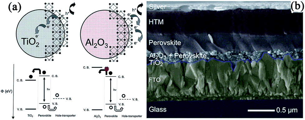 | ||
| Fig. 7 (a) The schematic of perovskite-coated TiO2 and Al2O3, illustrating electron and hole transfer. Reprinted with permission.13 (b) The schematic of MSSC with a thin Al2O3 layer. Reprinted with permission.67 | ||
In 2013, using a thin Al2O3 film (∼80 nm) processed at low temperature (<150 °C), Snaith et al. fabricated a “flat-junction” thin film solar cell with a thick perovskite “capping layer” on the top of the scaffold (see Fig. 7b), and improved the FTO/bl-TiO2/mp-Al2O3/MAPbI3−xClx/spiro-OMeTAD/Ag-based device efficiency to 12.3% (Jsc = 18 mA cm−2, Voc = 1.02 V, and FF = 0.67).67 Later, by incorporating core–shell Au@SiO2 nanoparticles (np-Au@SiO2) into the porous Al2O3 scaffold, the authors achieved significantly enhanced Jsc and PCE in the “Au@SiO2” device (Jsc = 16.91 mA cm−2, PCE = 11.4%) compared to the “Al2O3-only” device (Jsc = 14.76 mA cm−2, PCE = 10.7%), and introduced a new enhancement mechanism of reduced exciton binding energy with the incorporation of the metal nanoparticles, rather than enhanced light absorption.106 Worsley and coworkers reported a simplified one-step deposition process for the Al2O3–perovskite layer: a mixed DMF solution containing Al2O3 nanoparticles (np-Al2O3) and the MAPbI3−xClx perovskite precursor was directly spin-coated on the compact TiO2 layer, followed by a thermal treatment at low temperature (<110 °C).107 The device based on this co-deposited Al2O3–perovskite film, in which 5 wt% alumina was added to the precursor solution prior to spin-coating, yielded the highest PCE of 7.16%, with a Jsc of 12.78 mA cm−2, Voc of 0.925 V, and FF of 0.61. In 2014, Snaith and coworkers introduced a method to passivate the hole trapping states at the perovskite (MAPbI3−xClx) surface by assembling iodopentafluorobenzene (IPFB) via supramolecular halogen bonding.108 The passivation of the undercoordinated halides effectively reduced the density of accumulated charge at the perovskite/HTM heterojunction, leading to an increased FF (0.67) compared to that (0.57) in the unpassivated device and a high PCE of 15.7%. Later, using a low Al-doped TiO2 blocking layer (0.3 mol%), the authors also observed an increased Jsc (20 mA cm−2) and PCE (13.8%) compared with the undoped device (Jsc = 16.04 mA cm−2, PCE = 11.13%) due to the improved conductivity of Al-doped TiO2.109 Recently, by replacing the organic HTM with P3HT-functionalized single-walled carbon nanotubes (SWNTs) embedded in an insulating poly(methyl methacrylate) (PMMA) matrix, an MSSC device with unprecedented resilience against thermal stressing and moisture ingress was fabricated, and yielded a PCE of 15.3% with an average efficiency of 10 ± 2%.110
In spite of the elimination of high temperature sintering steps for the mesoporous Al2O3 scaffold, a high sintering temperature is still needed for the compact TiO2 layer (∼500 °C) in MSSCs, which lacks the compatibility with flexible substrates and thus presents a drawback in view of large scale industrial manufacture. In the end of 2013, by spin-coating the nanocomposites of graphene nanoflakes/TiO2 nanoparticles on the top of FTO-coated substrates, Snaith and coworkers fabricated low temperature processed electron collection layers at 150 °C.111 The superior charge mobility and proper work function of graphene effectively improved the electrical conductivity and reduced the formation of energy barriers at the material interfaces, leading to an excellent device efficiency of 15.6%. Subsequently, the authors reported a new route for fabricating a low temperature processed TiO2 compact layer (<150 °C). Compared with the previous MSSCs based on a high temperature sintered compact TiO2 layer, this all-low-temperature processed device yielded a PCE of up to 15.9%, with a Jsc of 21.5 mA cm−2, Voc of 1.02 V, and FF of 0.71 under simulated AM1.5 100 mW cm−2 sunlight. Also, the PCE of 15.9% is the highest reported value for Al2O3-based MSSCs.22 Furthermore, Yuan and coworkers also reported the use of compact ZnO layers which were fabricated by ALD at 70 °C, and achieved PCEs of 13.1% under standard AM1.5 illumination.112
Besides the Al2O3-based MSSCs, in 2013, Johansson46 and Park113et al. reported another type of MSSC based on a nanostructured ZrO2 scaffold. Like Al2O3, the much higher conduction band of ZrO2 than that of perovskite blocks the electron injection with no charge separation at the ZrO2/perovskite interface. Finally, using the SDP method, a PCE of 10.8% was achieved from this mp-ZrO2/MAPbI3-based device, with a high Voc up to 1.07 V. In 2014, Jiang and coworkers also fabricated a scaffold layer composed of SiO2 nanoparticles for perovskite solar cells.114 By controlling the size of the SiO2 nanoparticles, optimal FTO/bl-TiO2/mp-SiO2/MAPbI3−xClx/spiro-OMeTAD/Au-based devices yielded a PCE of 11.45%, with a Jsc of 16.4 mA cm−2, Voc of 1.05 V, and FF of 0.66.
| PL | DP | Device structure | J sc (mA cm−2) | V oc (V) | FF (%) | PCE (%) | Ref. |
|---|---|---|---|---|---|---|---|
| MAPbI3−xClx | OSPD | FTO/bl-TiO2/mp-Al2O3/PL/spiro/Ag | 17.8 | 0.98 | 63 | 10.9 | 13 |
| MAPbI3−xClx | OSPD | FTO/bl-TiO2/mp-Al2O3/PL/spiro/Ag | 18 | 1.02 | 67 | 12.3 | 67 |
| MAPbI3−xClx | OSPD | FTO/bl-TiO2/mp-Al2O3(np-Au@SiO2)/PL/spiro/Ag | 16.91 | 1.02 | 64 | 11.4 | 106 |
| MAPbI3−xClx | OSPD | FTO/bl-TiO2/PL(np-Al2O3)/spiro/Au | 12.78 | 0.925 | 61 | 7.16 | 107 |
| MAPbI3−xClx | OSPD | FTO/bl-TiO2/mp-Al2O3/PL/IPFB/spiro/Ag | 23.38 | 1.06 | 67 | 15.7 | 108 |
| MAPbI3−xClx | OSPD | FTO/bl-TiO2(Al)/mp-Al2O3/PL/spiro/Ag | 20 | 1.07 | 65 | 13.8 | 109 |
| MAPbI3−xClx | OSPD | FTO/bl-TiO2/mp-Al2O3/PL/P3HT-SWNTs-PMMA/Ag | 22.71 | 1.02 | 66 | 15.3 | 110 |
| MAPbI3−xClx | OSPD | FTO/bl-TiO2(graphene)/mp-Al2O3/PL/spiro/Au | 21.9 | 1.04 | 73 | 15.6 | 111 |
| MAPbI3−xClx | OSPD | FTO/bl-TiO2/mp-Al2O3/PL/spiro/Ag | 21.5 | 1.02 | 71 | 15.9 | 22 |
| MAPbI3 | OSPD | FTO/bl-ZnO/mp-Al2O3/PL/spiro/Ag | 20.4 | 0.976 | 66 | 13.1 | 112 |
| MAPbI3 | SDP | FTO/bl-TiO2/mp-ZrO2/PL/spiro/Ag | 17.3 | 1.07 | 59 | 10.8 | 46 |
| MAPbI3−xClx | OSPD | FTO/bl-TiO2/mp-SiO2/PL/spiro/Au | 16.4 | 1.05 | 66 | 11.45 | 114 |
4.3 Planar heterojunction perovskite solar cells
During the initial studies on MSSCs with an Al2O3 scaffold, Snaith and coworkers also fabricated a planar heterojunction perovskite solar cell based on a simple FTO/bl-TiO2/MAPbI3−xClx/spiro-OMeTAD/Ag structure. No porous metal-oxide structure was needed in this configuration and perovskite actually functioned as the ambipolar layer in a p–i–n junction, where the intrinsic (i) layer is the perovskite absorber. Preliminary research findings yielded PCEs from 1.8% (ref. 13) to 4.9%,67 and nearly 100% internal quantum efficiency (IQE) was measured.67 Also, it has been discovered that the typical 3-D organolead trihalide perovskites exhibit large charge carrier diffusion lengths (∼100 nm for the triiodide perovskite and >1 μm for the mixed halide perovskite with Cl).115,116 All the above mentioned studies indicate the possibility of this planar configuration to be a highly efficient architecture. In fact, the PHJ structure can not only simplify the device fabrication process but also avoid the pore filling problem in the mesosuperstucture device, which always leads to a large standard deviation. At present, two configurations for this planar device including a positive and inverted structure have been reported, in which a n-type (e.g. TiO2, ZnO) or p-type conductor (e.g. PEDOT:PSS, NiO, CuSCN, graphene oxide, polythiophene) was coated on a conductive glass, and both yielded excellent PCEs.In 2013, Kelly and coworkers reported the use of a thin ZnO nanoparticle film (∼25 nm) as an electron-transport layer in an ITO/bl-ZnO/MAPbI3/spiro-OMeTAD/Ag structure PHJ solar cell.47 The higher electron mobility of ZnO than TiO2 (ref. 92) and the large crystallite size on the surface of the ITO/bl-ZnO/MAPbI3 layer resulted in a higher Jsc (20.4 mA cm−2) with a PCE of 15.7%. Considering that no sintering or annealing step is required for fabricating the ZnO layer, the device on a flexible ITO/PET substrate was prepared, yielding a Voc of 1.03 V, Jsc of 13.4 mA cm−2, FF of 0.739 and PCE of 10.2%. Also, the PCE of 10.2% was the highest value in the reported flexible perovskite devices. Later, Lee et al. used a simple PC60BM modified, sol–gel processed ZnO layer as the electron conductor.118 Through this interfacial engineering, higher Voc values were observed in devices with bl-ZnO/PC60BM substrates compared to devices with only ZnO, and a PCE of 12.2% was achieved in ITO/bl-ZnO/PC60BM/MAPbI3/spiro-OMeTAD/MoO3/Ag-based devices. Bai and coworkers also reported low-temperature magnetron sputtered ZnO nanorod film as the cathode interlayer for ITO/bl-ZnO/MAPbI3/spiro-OMeTAD/MoO3/Ag-based device and achieved PCEs of 13.4% and 8.03% respectively in glass/ITO- and PET/ITO-based substrates.119
Besides the above-mentioned TiO2 or ZnO-based positive devices using spiro-OMeTAD as the HTM, other types of p–i–n junctions with different p-type HTMs such as organic P3HT,63,64PTB7-Th,118DR3TBDTT120 and inorganic CuSCN121 were also reported, with favorable performance achieved.
Very recently, through a method of Lewis base passivation,122 in which the crystal surfaces were treated with the Lewis bases thiophene and pyridine, a significant decrease in the rate of nonradiative recombination in perovskite films was measured by Snaith et al. The authors thought that the under-coordinated Pb ions in the perovskite crystal could be bound with Lewis base molecules, thus passivating these defect sites. At last, PCEs of 15.3% and 16.5% were achieved using thiophene and pyridine treated MAPbI3−xClx respectively in the FTO/bl-TiO2/MAPbI3−xClx/Lewis base/spiro-OMeTAD/Au-based device. Yang's group fabricated a modified planar configuration with an ITO/PEIE/bl-TiO2(Y)/MAPbI3−xClx/spiro-OMeTAD/Au structure, in which ITO was coated with polyethyleneimine ethoxylated (PEIE) while TiO2 was doped with yttrium (Y) (see Fig. 8).23 The PEIE-modified ITO effectively reduces the work function of ITO from 4.6 eV to 4.0 eV, which is beneficial to the efficient electron transport between the TiO2 and ITO layers. Also, like the Al-doped ZnO mentioned above,98 the doping of TiO2 with Y not only improves the conductivity (from 6 × 10⁻⁶ S cm−1 to 2 × 10⁻⁵ S cm−1) but also raises the Fermi level in the Y–TiO2 layer. At last, this all-low-temperature processed device yielded a record PCE of 19.3% with an average PCE of 16.6%.
 | ||
| Fig. 8 (a) SEM cross-sectional image of the device. (b) Diagram of energy levels (relative to the vacuum level) of each functional layer in the device. (c) J–V curves for the champion cell without antireflective coating. Reprinted with permission.23 | ||
| PL | PL thickness (nm) | DP | Device structure | J sc (mA cm−2) | V oc (V) | FF (%) | PCE (%) | Ref. |
|---|---|---|---|---|---|---|---|---|
| MAPbI3−xClx | 400–800 | OSPD | FTO/bl-TiO2/PL/spiro/Au | 20.3 | 0.89 | 64 | 11.4 | 31 |
| MAPbI3−xClx | ∼330 | DSVD | FTO/bl-TiO2/PL/spiro/Ag | 21.5 | 1.07 | 67 | 15.4 | 19 |
| MAPbI3−xClx | ∼400 | SDP | FTO/bl-TiO2/PL/spiro/Au | 22.9 | 0.98 | 69 | 14.82 | 43 and 117 |
| MAPbI3 | ∼350 | VASP | FTO/bl-TiO2/PL/spiro/Ag | 19.8 | 0.924 | 66.3 | 12.1 | 48 |
| MAPbI3 | ∼300 | SDP | FTO/bl-TiO2(rutile)/PL/spiro/Au | 19.8 | 1.05 | 64 | 13.7 | 66 |
| MAPbI3 | ∼300 | SDP | FTO/bl-TiO2/PL/spiro/Au | 20.71 | 1.02 | 64 | 13.5 | 41 |
| MAPbI3 | ∼350 | OSPD | FTO/bl-TiO2/PL/spiro/Ag | 21.1 | 1.04 | 74 | 16.2 | 27 |
| MAPbI3 | ∼300 | SDP | ITO/bl-ZnO/PL/spiro/Ag | 20.4 | 1.03 | 74.9 | 15.7 | 47 |
| MAPbI3 | ∼300 | SDP | PET/ITO/bl-ZnO/PL/spiro/Ag | 13.4 | 1.03 | 73.9 | 10.2 | |
| MAPbI3 | NA | SDP | ITO/bl-ZnO/PC60BM/PL/spiro/MoO3/Ag | 18.18 | 1.00 | 67 | 12.2 | 118 |
| MAPbI3 | NA | SDP | ITO/bl-ZnO/PL/spiro/MoO3/Ag | 22.4 | 1.04 | 57.4 | 13.4 | 119 |
| MAPbI3 | NA | SDP | PET/ITO/bl-ZnO/PL/spiro/MoO3/Ag | 18.4 | 0.87 | 49.7 | 8.03 | |
| MAPbI3−xClx | NA | OSPD | ITO/bl-TiO2/PL/P3HT/Ag | 21 | 0.936 | 69.1 | 13.6 | 63 and 64 |
| MAPbI3 | NA | SDP | ITO/bl-ZnO/PC60BM/PL/PTB7-Th/MoO3/Ag | 15.1 | 1.03 | 71 | 11.04 | 118 |
| MAPbI3−xClx | ∼350 | SDP | FTO/bl-TiO2/PL/DR3TBDTT/Au | 15.3 | 0.95 | 60 | 8.8 | 120 |
| MAPbI3 | ∼400 | OSPD | FTO/bl-TiO2/PL/CuSCN/Au | 14.4 | 0.727 | 61.7 | 6.4 | 121 |
| MAPbI3−xClx | NA | OSPD | FTO/bl-TiO2/MAPbI3−xClx/thiophene/spiro/Au | 21.3 | 1.02 | 68 | 15.3 | 122 |
| MAPbI3−xClx | NA | OSPD | FTO/bl-TiO2/MAPbI3−xClx/pyridine/spiro/Au | 24.1 | 1.05 | 72 | 16.5 | |
| MAPbI3−xClx | ∼350 | OSPD | ITO/PEIE/bl-TiO2(Y)/PL/spiro/Au | 22.75 | 1.13 | 75.01 | 19.3 | 23 |
Around the same time, Snaith, Bolink, and Yang reported independently several perovskite PHJ solar cells with high PCEs up to or over 10%. Snaith et al. demonstrated a device structure consisting of FTO/PEDOT:PSS/MAPbI3−xClx/PC60BM/TiOx/Al in which a bilayer of PC60BM and compact-TiOx were employed as the n-type charge collection layer.125 A PCE of 9.8% was obtained, with a Jsc of 15.8 mA cm−2, Voc of 0.94 V, and FF of 0.66. Also, a PCE of 6.4% was achieved for the same configuration on an ITO-coated PET plastic foil. Interestingly, when fabricating devices on ITO-covered glass, an obvious decrease of Jsc and FF was observed which arises likely from poorer perovskite film formation and lower surface coverage upon the PEDOT:PSS-coated ITO than on the PEDOT:PSS-coated FTO. Bolink et al. reported a MAPbI3 perovskite solar cell in which a highly oriented pure MAPbI3 film was sandwiched between an electron-blocking poly-TPD layer and a hole-blocking PC60BM layer (ITO/PEDOT:PSS/poly-TPD/MAPbI3/PC60BM/Au).126 A high Jsc of 16.12 mA cm−2 and Voc of 1.05 V revealed that very few electrons and holes recombine and at last, a PCE of 12.04% (cell area = 0.09 cm2) was achieved at the standard solar AM1.5G intensity of 100 mW cm−2 (the PCE was further improved to 14.8% with a 0.065 cm2 solar cell127). Yang and coworkers also fabricated two PHJ devices based on ITO/PEDOT:PSS/MAPbI3−xClx/PC60BM/Al and ITO/PEDOT:PSS/MAPbI3−xClx/ZnO/Al, yielding PCEs of 11.5% and 10.53% in a rigid substrate, respectively (a 9.2% efficiency was achieved in PET/ITO/PEDOT:PSS/MAPbI3−xClx/PC60BM/Al-based flexible devices).128 Later, Jen et al. reported a simple way to enhance the crystallization of solution-processed perovskite by incorporating additives into its precursor solution to modulate thin film formation.35 The device derived from the 1% DIO solution (FTO/PEDOT:PSS/MAPbI3−xClx/PC60BM/Bis-C60/Ag) exhibited a PCE of 11.8%, with a Jsc of 17.5 mA cm−2, Voc of 0.92 V, and FF of 0.73, compared to the 9.0% PCE of the device without using DIO. Similar enhancement was observed in the case of ITO substrates. Also, the relatively lower performance of the ITO-based device than the FTO-based device was consistent with Snaith's experiment. Lee et al. used a new self-organized hole extraction layer, which was composed of PEDOT:PSS and a perfluorinated ionomer (PFI) to modify the interface work function and then reduce the potential energy loss.129 The device based on an ITO/PEDOT:PSS/PFI/MAPbI3/PC60BM/Al structure yielded an enhanced performance (PCE = 11.7%, Jsc = 16.7 mA cm−2, Voc = 0.982 V, FF = 0.705) compared to that of an ITO/PEDOT:PSS/MAPbI3/PC60BM/Al-based device (PCE = 8.1%, Jsc = 14.1 mA cm−2, Voc = 0.835 V, FF = 0.685). Also, 8.0% efficiency was achieved in flexible perovskite solar cells with this self-organized hole extraction layer on a PET/ITO substrate. Seok and coworkers also used a solvent-engineering technology, which employed a mixture solution of DMSO:GBL (3:7, v/v), to fabricate the uniform and dense perovskite layer, and further improved the PCE to 14.1% in ITO/PEDOT:PSS/MAPbI3/PC60BM/LiF/Al-based devices.26
Huang and coworkers fabricated two types of PHJ perovskite solar cells with an ITO/PEDOT:PSS/MAPbI3/PC60BM/C60/BCP/Al or ITO/PEDOT:PSS/MAPbI3/IC60BA/C60/BCP/Al structure (see Fig. 9).130 A unique double fullerene layer was adopted in these devices which could effectively reduce dark current leakage by forming a Schottky junction with the anode. By varying the ratio and concentration of the precursor solutions, the morphology, absorption and crystallization of perovskite films could be tuned and at last, an optimal device with an IC60BA acceptor layer exhibited the best PCE of 12.2%, with a Jsc of 15.7 mA cm−2, Voc of 0.97 V, and FF of 0.80. Later, using a new film forming method by interdiffusion of spin-coated stacking layers of PbI2 and MAI (via TSSD), a high quality film was achieved by Huang et al.49 Perovskite based on an ITO/PEDOT:PSS/MAPbI3/PC60BM/C60/BCP/Al system gave a PCE of 15.3%, with a relatively high Jsc of 20.59 mA cm−2 under AM 1.5 simulated one sun illumination (further optimization using solvent annealing yielded a PCE of 15.6% with a perovskite thickness of 630 nm (ref. 131). Recently, Lin56 and Wu50 also obtained high PCEs of 15.4% and 16.3% in ITO/PEDOT:PSS/MAPbI3−xClx/C60/Bphen/Ca/Ag-based and ITO/PEDOT:PSS/MAPbI3/PC70BM/Ca/Al-based devices using SVD or TSSD.
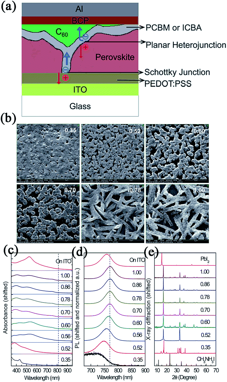 | ||
| Fig. 9 (a) The schematic of the device structure. (b) Top view SEM images. (c) Absorption spectra. (d) Photoluminescence spectra and (e) XRD patterns of the iodine perovskite films spun from solutions with a precursor ratio from 0.35 to 1. Reprinted with permission.130 | ||
Apart from the most widely used PEDOT:PSS, in early 2014, Guo and coworkers replaced the PEDOT:PSS layer with a thin NiOx interlayer (∼10 nm).102 The device containing ITO/NiOx/MAPbI3/C60/BCP/Al and ITO/NiOx/MAPbI3/PC60BM/BCP/Al showed PCEs of 5.7% and 7.8% respectively with enhanced Voc compared to devices using the PEDOT:PSS layer. The authors attributed this to the low energy loss for holes in the NiOx/MAPbI3 junction and a better surface coverage of MAPbI3 film on the glass/ITO/NiOx substrate. Sarkar and coworkers also reported two types of MAPbI3−xClx perovskite solar cells with a FTO/NiO/MAPbI3−xClx/PC60BM/Ag or FTO/CuSCN/MAPbI3−xClx/PC60BM/Ag structure.132 Devices with this electrodeposited NiO film and CuSCN film exhibited a PCE of 7.26% and 3.8%, respectively. Later, Yang et al. used a sol–gel process to fabricate a thin NiO nanocrystalline film (∼40 nm) for the development of a FTO/NiO/MAPbI3/PC60BM/Au-based solar cell, and further improved the PCE to 9.11%.133 Recently, by using a thin graphene oxide (GO) (∼2 nm)134 or polythiophene (PT) (∼18 nm)135 layer as a new p-type conductor instead of PEDOT:PSS, PCEs of 12.4% and 11.8% were achieved in ITO/GO/MAPbI3−xClx/PC60BM/ZnO/Al and ITO/PT/MAPbI3/C60/BCP/Ag-based devices, respectively.
| PL | PL thickness (nm) | DP | Device structure | J sc (mA cm−2) | V oc (V) | FF (%) | PCE (%) | Ref. |
|---|---|---|---|---|---|---|---|---|
| a With 1% DIO. | ||||||||
| MAPbI3 | 20–30 | OSPD | ITO/PEDOT:PSS/PL/C60/BCP/Al | 9.02 | 0.55 | 61 | 3.0 | 123 |
| MAPbI3 | 20–30 | OSPD | ITO/PEDOT:PSS/PL/PC60BM/BCP/Al | 10.32 | 0.60 | 63 | 3.9 | |
| MAPbI3 | 20–30 | OSPD | ITO/PEDOT:PSS/PL/IC60BA/BCP/Al | 10.03 | 0.58 | 58 | 3.4 | |
| MAPbI3 | 50 ± 5 | OSPD | ITO/PEDOT:PSS/PL/PC60BM/Al | 8.2 | 0.82 | 77 | 5.2 | 124 |
| MAPbI3 | 110 ± 5 | SDP | ITO/PEDOT:PSS/PL/PC60BM/Al | 10.8 | 0.91 | 76 | 7.4 | |
| MAPbI3−xClx | 300–400 | OSPD | FTO/PEDOT:PSS/PL/PC60BM/TiOx/Al | 15.8 | 0.94 | 66 | 9.8 | 125 |
| MAPbI3−xClx | 300–400 | OSPD | ITO/PEDOT:PSS/PL/PC60BM/TiOx/Al | 14.4 | 0.92 | 47 | 6.3 | |
| MAPbI3−xClx | 300–400 | OSPD | PET/ITO/PEDOT:PSS/PL/PC60BM/TiOx/Al | 14.4 | 0.88 | 51 | 6.4 | |
| MAPbI3 | ∼285 | DSVD | ITO/PEDOT:PSS/poly-TPD/PL PC60BM/Au | 16.12 | 1.05 | 67 | 12.04 | 126 |
| MAPbI3−xClx | ∼340 | OSPD | ITO/PEDOT:PSS/PL/PC60BM/Al | 18.5 | 0.87 | 72 | 11.5 | 128 |
| MAPbI3−xClx | ∼340 | OSPD | ITO/PEDOT:PSS/PL/ZnO/Al | 17.29 | 0.886 | 68.76 | 10.53 | |
| MAPbI3−xClx | ∼340 | OSPD | PET/ITO/PEDOT:PSS/PL/PC60BM/Al | 16.5 | 0.86 | 64 | 9.2 | |
| MAPbI3−xClx | ∼400 | OSPD | ITO/PEDOT:PSS/PL/PC60BM/Bis-C60/Ag | 15 | 0.90 | 58 | 7.9 | 35 |
| MAPbI3−xClx | ∼400 | OSPD | ITO/PEDOT:PSS/PL/PC60BM/Bis-C60/Ag | 15.6 | 0.92 | 71 | 10.3 | |
| MAPbI3−xClx | ∼400 | OSPD | FTO/PEDOT:PSS/PL/PC60BM/Bis-C60/Ag | 16 | 0.90 | 62 | 9 | |
| MAPbI3−xClx | ∼400 | OSPD | FTO/PEDOT:PSS/PL/PC60BM/Bis-C60/Ag | 17.5 | 0.92 | 73 | 11.8 | |
| MAPbI3 | NA | TSSD | ITO/PEDOT:PSS/PFI/PL/PC60BM/Al | 16.7 | 0.982 | 70.5 | 11.7 | 129 |
| MAPbI3 | NA | TSSD | PET/ITO/PEDOT:PSS/PFI/PL/PC60BM/Al | 15.5 | 1.04 | 49.9 | 8.0 | |
| MAPbI3 | ∼290 | OSPD | ITO/PEDOT:PSS/PL/PC60BM/LiF/Al | 20.7 | 0.886 | 78.3 | 14.1 | 26 |
| MAPbI3 | ∼140 | OSPD | ITO/PEDOT:PSS/PL/PC60BM/C60/BCP/Al | 15.9 | 0.88 | 72.2 | 10.1 | 130 |
| MAPbI3 | ∼140 | OSPD | ITO/PEDOT:PSS/PL/IC60BA/C60/BCP/Al | 15.7 | 0.97 | 80.1 | 12.2 | |
| MAPbI3 | 270–300 | TSSD | ITO/PEDOT:PSS/PL/PC60BM/C60/BCP/Al | 19.6 | 0.99 | 79.3 | 15.4 | 49 |
| MAPbI3 | ∼630 | TSSD | ITO/PEDOT:PSS/PL/PC60BM/C60/BCP/Al | 21.0 ± 0.5 | 0.96 ± 0.02 | 76.0 ± 1.5 | 15.6 | 131 |
| MAPbI3−xClx | ∼430 | SVD | ITO/PEDOT:PSS/PL/C60/Bphen/Ca/Ag | 20.9 | 1.02 | 72.2 | 15.4 | 56 |
| MAPbI3 | ∼360 | TSSD | ITO/PEDOT:PSS/PL/PC70BM/Ca/Al | 19.98 | 1.05 | 78 | 16.31 | 50 |
| MAPbI3 | ∼60 | OSPD | ITO/NiOx/PL/C60/BCP/Al | 12.95 | 0.74 | 60 | 5.7 | 102 |
| MAPbI3 | ∼60 | OSPD | ITO/NiOx/PL/PC60BM/BCP/Al | 12.43 | 0.92 | 68 | 7.8 | |
| MAPbI3−xClx | NA | DSVD | FTO/NiO/PL/PC60BM/Ag | 14.2 | 0.786 | 65 | 7.26 | 132 |
| MAPbI3−xClx | NA | DSVD | FTO/CuSCN/PL/PC60BM/Ag | NA | NA | NA | 3.8 | |
| MAPbI3 | ∼250 | SDP | FTO/NiO/PL/PC60BM/Au | 16.27 | 0.882 | 63.5 | 9.11 | 133 |
| MAPbI3−xClx | ∼170 | OSPD | ITO/GO/PL/PC60BM/ZnO/Al | 17.46 | 1.00 | 71 | 12.40 | 134 |
| MAPbI3 | 250 ± 20 | SDP | ITO/PT/PL/C60/BCP/Ag | 16.2 | 1.03 | 70.7 | 11.8 | 135 |
5. Hole-transporting materials (HTMs) for perovskite solar cells
Despite the rapid increase in efficiency associated with the evolution of different types of perovskites and device fabrication techniques, the development of HTM is very limited and mainly focused on organic compounds. In particular, the bulky 3-D spiro-OMeTAD (see Fig. 10) with the twisted spirobifluorene center has been proven as the most potential hole conductor for state-of-the-art perovskite-based devices since it was firstly introduced in 1998 for ss-DSSCs.10 So far, based on spiro-OMeTAD HTM, MMOPSCs,21 MSSCs22 and PHJPSCs23 have respectively showed their best device performance. However, the tedious synthesis of spiro-OMeTAD represents a potential hurdle for future commercialization due to its high cost. So looking for new kinds of alternative HTMs to spiro-OMeTAD with a simpler synthetic route, lower production cost and comparable device performance is very necessary. Also, a compatible HOMO energy level relative to perovskites and high charge-carrier mobility should also be considered. In the past two years, many new-type HTMs, including organic small molecules, polymers and inorganic materials, have been used for perovskite solar cells and promising performance has been achieved for the corresponding devices. | ||
| Fig. 10 The chemical structure of spiro-OMeTAD. | ||
5.1 HTMs based on small molecules (Table 6)
Early in 2013, Hodes and coworkers employed a small molecule TPD as the HTM for perovskite solar cells with MAPbBr3-coated alumina scaffolds and achieved a low PCE of 0.67%.105 Later, Johansson et al. reported a small molecule hole conductor DEH for fabricating MAPbI3 perovskite solar cells, and found that, compared with the spiro-OMeTAD-based device, the device with DEH showed a faster recombination rate (∼100 times higher), leading to a decreased performance with a low PCE of 1.6%.136 The authors suggested that for perovskite solar cells, the molecular structure of the HTM should be designed to block close contact between the perovskite and the hole on the HTM, which favors reduction of electronic coupling and charge recombination. Thus molecules with a bulky, twisty 3-D structure (e.g. phenylamine) may be a potential choice for future HTMs.
In the end of 2013, by replacing the spirobifluorene core of spiro-OMeTAD with a pyrene core, three HTMs based on pyrene-core arylamine derivatives, Py-A, Py-B and Py-C, were investigated by Seok et al.137 Comparable Jsc (∼20 mA cm−2) and PCE (∼12%) were observed in the cells fabricated with Py-B and Py-C, while the Py-A-based device showed low performance (Jsc = 10.8 mA cm−2, PCE = 3.3%), which was due to the insufficient driving force for hole injection from MAPbI3 (−5.44 eV) to Py-A (−5.41 eV). The optimal device based on Py-B and Py-C demonstrated PCEs of 12.3% and 12.4%, respectively, showing the possibility of using HTMs with the new structure instead of spiro-OMeTAD for efficient and low-cost organometal halide perovskite solar cells. Subsequently, a series of dumbbell-shaped or star-shaped molecules with phenylamine derivatives, especially triphenylamine (TPA), as the terminal group or core were synthesized and some of them exhibited comparable device performance to that of spiro-OMeTAD-based perovskite solar cells.
In 2014, Mhaisalkar and coworkers developed two thiophene/TPA-based HTMs H101138 and KTM3,139 incorporating 3,4-ethylenedioxythiophene or swivel-cruciform 3,3-bithiophene as the core unit terminated with two or four TPAs. Through appropriate chemical doping with tris(2-(1H-pyrazol-1-yl)pyridine)cobalt(III) tris(hexafluorophosphate) (FK102) (for H101) or bis(2,6-di(1H-pyrazol-1-yl)pyridine)cobalt(III) tris(bis(trifluoromethylsulfonyl)-imide) (FK269) (for KTM3), optimal mesoporous devices based on H101 or KTM3 yielded PCEs of 13.8% or 11%, respectively under AM1.5G solar simulation (100 mW cm−2). After that, the authors reported three star-shaped HTMs (T101, T102 and T103) based on a rigid triptycene central core.140 The HOMO levels of T101, T102 and T103 calculated from CV are −5.29, −5.35 and −5.33 eV, respectively, which are lower than that of spiro-OMeTAD (−5.22 eV). By modifying the linkage form between triptycene and diphenylamine groups, devices based on T101, T102 and T103 yielded PCEs of 8.42%, 12.24% and 12.38%, respectively with relatively high Voc. Ko et al. also reported two star-shaped HTMs OMeTPA-TPA and OMeTPA-FA with an incorporated fused quinolizino acridine or TPA as a core unit.141 Devices comprising FTO/bl-TiO2/mp-TiO2/MAPbI3/OMeTPA-TPA/Au and FTO/bl-TiO2/mp-TiO2/MAPbI3/OMeTPA-FA/Au demonstrated PCEs of 12.31% and 13.63% using three dopants composed of 4-tert-butylpyridine (TBP), bis(trifluoromethane)sulfonimide lithium salt (LiTFSI), and tris(2-(1H-pyrazol-1-yl)-4-tert-butylpyridine)cobalt(III) tris(bis(trifluoromethylsulfonyl)imide) (FK209) into the HTMs. A noteworthy feature is that even without any p-type additives, a high PCE of 11.7% was still achieved in the OMeTPA-FA-based device. Later, Meng and coworkers developed two simple HTMs TPBS and TPBC by introducing electron-donating groups asymmetrically into the N,N,N′,N′-tetraphenyl-benzidine core, and achieved impressive PCEs of 10.29% and 13.10% respectively in TPBS- and TPBC-based devices without any doping.142
Recently, Sun and coworkers fabricated FTO/bl-TiO2/mp-TiO2/MAPbI3−xClx/HTM/Ag-based perovskite solar cells using two carbazole-based small molecules X19 and X51 as HTMs.143 Almost three times higher hole mobilities than that of spiro-OMeTAD (X19: 1.19 × 10⁻⁴ cm2 V−1 s−1, X51: 1.51 × 10⁻⁴ cm2 V−1 s−1, spiro-OMeTAD: 5.31 × 10⁻⁵ cm2 V−1 s−1) were measured for these two materials. Optimal devices with X19 and X51 HTMs yielded PCEs of 7.6% and 9.8% under AM1.5G (100 mW cm−2) illumination. Lee et al. reported the synthesis and characterization of three carbazole-based HTMs with two-arm and three-arm type structures SGT-404. SGT-405 and SGT-407, which are linked through phenylene, diphenylene or triphenyl amine derived core units.144 FTO/bl-TiO2/mp-TiO2/MAPbI3/HTM/Au-based devices yielded high efficiencies of 13.28% (SGT-404), 14.79% (SGT-405) and 13.86% (SGT-407), which were comparable to that of the device employing commercial spiro-OMeTAD (15.23%).
Xiao and coworkers synthesized a series of HTMs based on a diphenyl core with TPA as the terminal group bridged with olefinic bonds of different lengths, which is the first case of adoption of small molecule HTMs with a linear π-conjugated structure.145 Without any dopant for HTMs, the FTO/TiO2/MAPbI3/2TPA-2-DP/Au solar cell exhibits an encouraging PCE of 9.1%, with a Voc of 0.94 V, Jsc of 16.3 mA cm−2, and FF of 0.597. Meng et al. reported two TPA-based hole conductors HTM1 and HTM2 containing butadiene derivatives.146 Both of them exhibited high hole mobilities, which were 2.98 × 10⁻³ cm2 V−1 s−1 for HTM1 and 1.27 × 10⁻³ cm2 V−1 s−1 for HTM2. MAPbI3 perovskite solar cells showed a PCE of 11.34% for HTM1 and 11.63% for HTM2, respectively. Later, the authors employed another low-cost, non-traditional TPA-based HTM PNBA in FTO/bl-TiO2/mp-TiO2/MAPbI3/PNBA/Au-based devices and achieved a PCE of 11.4%.147
Besides looking for alternative HTMs with new structures, studies based on the classic spiro-OMeTAD, such as structure optimization or energy level engineering, are still needed. In 2014, Seok et al. synthesized and reported two more spiro-OMeTAD isomers by replacing pareb (p)-OMe groups in spiro-OMeTAD (pp-spiro-OMeTAD) with ortho (o)- and meta (m)-OMe groups (which are named as po-spiro-OMeTAD and pm-spiro-OMeTAD, respectively; see Fig. 11).60 Similar Jsc and Voc were observed for the three pp-, pm-, and po-spiro-OMeTAD derivatives while po-spiro-OMeTAD showed the highest FF value which can be attributed to its low series resistance (Rs) and shunt resistance (Rsh). As a result, a higher PCE of 16.7% was obtained for the po-spiro-OMeTAD-based device compared with the classic pp-spiro-OMeTAD with a PCE of ∼15%. Leo and coworkers used five TPA-based HTMs (including MeO-TPD, spiro-MeO-TPD, spiro-TTB, spiro-TAD and BPAPF) with spiro-OMeTAD to correlate their HOMO energy levels with the Voc of the inverted planar MAPbI3−xClx-based devices, and highlighted the delicate energetic balance between the driving force for hole-extraction and maximizing the photovoltage (see Fig. 12).148
 | ||
| Fig. 11 A summary of small molecule HTMs based on phenylamine derivatives. | ||
 | ||
| Fig. 12 (a) Chemical structures of HTMs reported by Leo et al. (b) General device architecture and corresponding energy level diagram. Reprinted with permission.148 | ||
 | ||
| Fig. 13 A summary of small molecule HTMs without phenylamine derivatives. | ||
In 2014, Han and coworkers employed an alkyl-substituted tetrathiafulvalene TTF-1 as the HTM for an MAPbI3-based device.152 The long alkyl chains in TTF-1 not only improve its solubility for solution processes, but also maintain a certain amount of intermolecular stacking due to the fastener-effect of the long alkyl chains. No p-type dopants were added, and FTO/bl-TiO2/mp-TiO2/MAPbI3/TTF-1/Ag-based devices yielded a PCE of 11.03%, with a Jsc of 19.9 mA cm−2, Voc of 0.86 V, and FF of 0.644.
Xiao et al. reported a low band gap oligothiophene HTM named DR3TBDTT, containing benzodithiophene as the central block and ethylrhodanine as the end group.120 No ion additive was mixed into DR3TBDTT but for the addition of a small amount of insulated polydimethylsiloxane (PDMS), which acted as a flow agent to improve film formation of HTM on perovskites. Optimal PHJ devices with a FTO/bl-TiO2/MAPbI3−xClx/DR3TBDTT/Au structure yielded a PCE of 8.8% with excellent stability. Grätzel et al. also developed two more S,N-heteroacene-based dopant-free oligothiophenes G1 and G2 as HTMs for FTO/bl-TiO2/mp-TiO2/MAPbI3/HTM/Au-based perovskite solar cells, and achieved PCEs of 10.5% and 9.5%, respectively.150 Nazeeruddin and coworkers synthesized a flattened star-shaped molecule Fused-F with quinolizino acridine as the core.151 The device based on Fused-F achieved a high PCE of 12.8% under the illumination of 98.8 mW cm−2, with a Voc of 1.04 V, Jsc of 17.9 mA cm−2, and FF of 0.68 without any additives.
| HTM | E HOMO (eV) | p-Doping | Device structure | DP | J sc (mA cm−2) | V oc (V) | FF (%) | PCE (%) | Ref. |
|---|---|---|---|---|---|---|---|---|---|
| a1 | −5.3 | NA | FTO/bl-TiO2/mp-Al2O3/MAPbBr3/a1/Au | OSPD | 1.22 | 1.20 | 46 | 0.67 | 105 |
| a2 | NA | LiTFSI/TBP | FTO/bl-TiO2/mp-TiO2/MAPbI3/a2/Au | OSPD | NA | NA | NA | 1.6 | 136 |
| a3 | −5.41 | LiTFSI/TBP/FK209 | FTO/bl-TiO2/mp-TiO2/MAPbI3/a3/Au | OSPD | 10.8 | 0.89 | 34.6 | 3.3 | 137 |
| a4 | −5.25 | LiTFSI/TBP/FK209 | FTO/bl-TiO2/mp-TiO2/MAPbI3/a4/Au | OSPD | 20.4 | 0.95 | 63.7 | 12.3 | |
| a5 | −5.11 | LiTFSI/TBP/FK209 | FTO/bl-TiO2/mp-TiO2/MAPbI3/a5/Au | OSPD | 20.2 | 0.89 | 69.4 | 12.4 | |
| a6 | −5.16 | LiTFSI/TBP/FK102 | FTO/bl-TiO2/mp-TiO2/MAPbI3/a6/Au | SDP | 20.5 | 1.04 | 65 | 13.8 | 138 |
| a7 | −5.29 | LiTFSI/TBP/FK269 | FTO/bl-TiO2/mp-TiO2/MAPbI3/a7/Au | SDP | 13.0 | 1.08 | 78.3 | 11.0 | 139 |
| a8 | −5.29 | LiTFSI/TBP/FK102 | FTO/bl-TiO2/mp-TiO2/MAPbI3/a8/Au | SDP | 13.5 | 0.996 | 62.6 | 8.42 | 140 |
| a9 | −5.35 | LiTFSI/TBP/FK102 | FTO/bl-TiO2/mp-TiO2/MAPbI3/a9/Au | SDP | 17.2 | 1.03 | 69.1 | 12.24 | |
| a10 | −5.33 | LiTFSI/TBP/FK102 | FTO/bl-TiO2/mp-TiO2/MAPbI3/a10/Au | SDP | 20.3 | 0.985 | 61.9 | 12.38 | |
| a11 | −5.13 | LiTFSI/TBP/FK209 | FTO/bl-TiO2/mp-TiO2/MAPbI3/a11/Au | SDP | 20.88 | 0.946 | 62 | 12.31 | 141 |
| a12 | −5.14 | LiTFSI/TBP/FK209 | FTO/bl-TiO2/mp-TiO2/MAPbI3/a12/Au | SDP | 20.98 | 0.972 | 67 | 13.63 | |
| a13 | −5.30 | No dopant | FTO/bl-TiO2/mp-TiO2/MAPbI3/a13/Au | SDP | 15.75 | 0.932 | 70 | 10.29 | 142 |
| a14 | −5.33 | No dopant | FTO/bl-TiO2/mp-TiO2/MAPbI3/a14/Au | SDP | 19.32 | 0.942 | 72 | 13.10 | |
| a15 | NA | LiTFSI/TBP | FTO/bl-TiO2/mp-TiO2/MAPbI3−xClx/a15/Ag | OSPD | 17.14 | 0.76 | 58 | 7.6 | 143 |
| a16 | NA | LiTFSI/TBP | FTO/bl-TiO2/mp-TiO2/MAPbI3−xClx/a16/Ag | OSPD | 16.79 | 0.88 | 66 | 9.8 | |
| a17 | NA | LiTFSI/TBP/FK209 | FTO/bl-TiO2/mp-TiO2/MAPbI3/a17/Au | SDP | 19.76 | 0.963 | 69.8 | 13.28 | 144 |
| a18 | NA | LiTFSI/TBP/FK209 | FTO/bl-TiO2/mp-TiO2/MAPbI3/a18/Au | SDP | 20.28 | 1.023 | 71.3 | 14.79 | |
| a19 | NA | LiTFSI/TBP/FK209 | FTO/bl-TiO2/mp-TiO2/MAPbI3/a19/Au | SDP | 20.35 | 0.993 | 68.6 | 13.86 | |
| a20 | −4.96 | No dopant | FTO/bl-TiO2/mp-TiO2/MAPbI3/a20/Au | OSPD | 16.3 | 0.94 | 59.7 | 9.1 | 145 |
| a21 | −5.35 | NA | FTO/bl-TiO2/mp-TiO2/MAPbI3/a21/Au | SDP | 18.1 | 0.921 | 68 | 11.34 | 146 |
| a22 | −5.23 | NA | FTO/bl-TiO2/mp-TiO2/MAPbI3/a22/Au | SDP | 17.9 | 0.942 | 69 | 11.63 | |
| a23 | −5.42 | NA | FTO/bl-TiO2/mp-TiO2/MAPbI3/a23/Au | SDP | 17.5 | 0.945 | 68.9 | 11.4 | 147 |
| a24 | −5.31 | LiTFSI/TBP | FTO/bl-TiO2/mp-TiO2/MAPbI3/a24/Au | OSPD | 21.1 | 1.01 | 65.2 | 13.9 | 60 |
| a25 | −5.22 | LiTFSI/TBP | FTO/bl-TiO2/mp-TiO2/MAPbI3/a25/Au | OSPD | 21.2 | 1.02 | 77.6 | 16.7 | |
| spiro | −5.0 | F6-TCNNQ | ITO/dopant/spiro/MAPbI3−xClx/C60/Ag | DSVD | 14.4 | 0.795 | 69 | 7.8 | 148 |
| a26 | −5.1 | F6-TCNNQ | ITO/dopant/a26/MAPbI3−xClx/C60/Ag | DSVD | 14.9 | 0.863 | 69 | 8.7 | |
| a27 | −5.1 | F6-TCNNQ | ITO/dopant/a27/MAPbI3−xClx/C60/Ag | DSVD | 16 | 1.03 | 66 | 10.9 | |
| a28 | −5.3 | F6-TCNNQ | ITO/dopant/a28/MAPbI3−xClx/C60/Ag | DSVD | 16.1 | 0.968 | 70 | 10.9 | |
| a29 | −5.4 | F6-TCNNQ | ITO/dopant/a29/MAPbI3−xClx/C60/Ag | DSVD | 12.4 | 0.820 | 58 | 6.7 | |
| a30 | −5.6 | NDP9 | ITO/dopant/a30/MAPbI3−xClx/C60/Ag | DSVD | 0.72 | 0.835 | 13 | 0.08 | |
| b1 | −5.8 | NA | FTO/bl-TiO2/mp-Al2O3/MAPbBr3/b1/Au | OSPD | 1.08 | 1.30 | 40 | 0.56 | 105 |
| b1 | −5.8 | NA | FTO/bl-TiO2/mp-TiO2/MAPbBr3/b1/Au | OSPD | 1.14 | 1.00 | 41 | 0.47 | |
| b2 | −6.1 | NA | FTO/bl-TiO2/mp-Al2O3/MAPbBr3/b2/Au | OSPD | 1.57 | 1.06 | 43 | 0.72 | |
| b3 | −6.23 | LiTFSI/TBP | FTO/bl-TiO2/mp-Al2O3/MAPbBr3−xClx/b3/Au | OSPD | 4.0 | 1.50 | 46 | 2.7 | 149 |
| b4 | −5.05 | No dopant | FTO/bl-TiO2/mp-TiO2/MAPbI3/b4/Ag | SDP | 19.9 | 0.86 | 64.4 | 11.03 | 152 |
| b5 | −5.39 | PDMS | FTO/bl-TiO2/MAPbI3−xClx/b5/Au | SDP | 15.3 | 0.95 | 60 | 8.8 | 120 |
| b6 | −5.26 | No dopant | FTO/bl-TiO2/mp-TiO2/MAPbI3/b6/Au | SDP | 16.4 | 0.992 | 65 | 10.5 | 150 |
| b7 | −5.10 | No dopant | FTO/bl-TiO2/mp-TiO2/MAPbI3/b7/Au | SDP | 15.2 | 0.90 | 68 | 9.5 | |
| b8 | −5.23 | No dopant | FTO/bl-TiO2/mp-TiO2/MAPbI3/b8/Au | SDP | 17.9 | 1.04 | 68 | 12.8 | 151 |
5.2 HTMs based on polymers (Table 7 and Fig. 14)
As spiro-OMeTAD is the model material in small molecule HTMs, P3HT is the model material in polymer HTMs. In previous reports, low PCEs less than 1% were obtained by Hodes and Qiu et al. in the mp-TiO2/MAPbBr3/P3HT/Au- or mp-Al2O3/MAPbBr3/P3HT/Au-based devices.105,153 Later, by using MAPbI3 or MAPbI3−xClx instead of MAPbBr3 as the active layer, PCEs from 6.7% to over 13% were achieved by several groups,20,63,64,154–157 showing that P3HT can be a suitable HTM for efficient and low cost perovskite based solar cells. Bian and coworkers also used a thin polythiophene film prepared via electrochemical polymerization as the HTM in an ITO/PT/MAPbI3/C60/BCP/Ag-based device, and observed a PCE of 11.8%.135In 2013, Seok and coworkers reported the use of PTAA as the hole conductor for perovskite solar cells.20 A pillared structure consisting of 3-D composites of TiO2/MAPbI3 with partially infiltrated PTAA was observed and the optimized solar cell device based on FTO/bl-TiO2/mp-TiO2/MAPbI3/PTAA/Au exhibited a Jsc of 16.5 mA cm−2, Voc of 0.997 V and FF of 0.727, yielding a PCE of 12.0% under standard AM 1.5 conditions. Subsequently, two more triarylamine polymer derivatives containing fluorene and indenofluorene, named PF8-TAA, and PIF8-TAA, combined with PTAA, were studied to understand and optimize the Voc of the resulting perovskite solar cells with an architecture consisting of FTO/TiO2/MAPbBr3/HTM/Au or FTO/TiO2/MAPbI3/HTM/Au.158 Both the perovskite materials and the HOMO level of the HTM determine the high voltage output and at last, a PCE of 6.7% with a high Voc of 1.40 V was obtained in PIF8-TAA-based MAPbBr3 perovskite solar cells, which is the highest PCE reported for MAPbBr3 perovskite solar cells. Also, the PCE of the PTAA/MAPbI3-based device was further improved to 16.2%. Later, Yang and coworkers reported three polyfluorene derivatives, named PFO, TFB and PFB, as the HTMs in MAPbI3-based devices. The highest hole extraction rate of TFB was observed and the optimal device (FTO/bl-TiO2/mp-TiO2/MAPbI3/TFB/Au) yielded a PCE of 10.92% and 12.8% via the OSPD and SDP techniques.159 Grätzel et al. also developed a novel 2,4-dimethoxy-phenyl substituted triarylamine oligomer S197 as the HTM for FTO/bl-TiO2/mp-TiO2/MAPbI3/S197/Au-based device, and achieved comparable PCE (12%) with PTAA-based devices.160
Conjugated donor–accepter (D–A) copolymers are widely used in OPVs. D–A polymers with high hole mobility and an appropriate HOMO level can be potential HTM materials for perovskite solar cells. Seok et al. fabricated MAPbI3 perovskite solar cells with D–A copolymers PCPDTBT or PCDTBT as the HTM, in which benzothiadiazole was used as the acceptor and carbazole or cyclopentadithiophene as the donor.20 A PCE of 4.2% (Jsc = 10.5 mA cm−2, Voc = 0.92 V, FF = 0.437) was observed for PCDTBT and a PCE of 5.3% (Jsc = 10.3 mA cm−2, Voc = 0.77 V, FF = 0.667) was observed for PCPDTBT in FTO/bl-TiO2/mp-TiO2/MAPbI3/HTM/Au-based devices.
Qiu and Park et al. reported two diketopyrrolopyrrole-containing polymer HTMs PCBTDPP and PDPPDBTE. PCEs of 5.55% and 9.2% were obtained respectively by using a FTO/TiO2/MAPbI3/HTM/Au structure at 100 mA cm−2 illumination (AM1.5G);153,161 it is worth noting that without encapsulation, devices containing PCBTDPP or PDPPDBTE showed excellent long-term stability in air at room temperature, guaranteeing the practical applicability of these solid-state hybrid solar cells under outdoor working conditions.
Park and coworkers also investigated two D–A polymer HTMs PTB-BO and PTB-DCB21 and found that,162 compared with PTB-BO without a 3,4-dichlorobenzyl group, the introduction of functionalized PTB-DCB21 was more effective in accelerating electron transport and retarding charge recombination. As a result, under the condition of the absence of any additives, higher PCE of 8.7% was achieved for PTB-DCB21-based devices while PTB-BO-based devices showed a PCE of 7.4%. Recently, Lee et al. fabricated a PHJ perovskite solar cell using PTB7-Th as the HTM. Devices using an ITO/bl-ZnO/PC60BM/MAPbI3/PTB7-Th/MoO3/Ag structure yielded a PCE of 11.04%, with a Jsc of 15.1 mA cm−2, Voc of 1.03 V, and FF of 0.71.118
 | ||
| Fig. 14 A summary of polymer HTMs. | ||
However, despite the wide absorption of low band gap polymers, it has been proven that the role of polymers is only limited to a charge transporting layer rather than as a light harvester because no obvious contribution to external quantum efficiency is found in the long wavelength range. Recently, Snaith and coworkers combined a MAPbI3−xClx perovskite with a fullerene selfassembled monolayer (C60SAM) functionalized TiO2 to produce a dual absorbing, perovskite–polymer HTM hybrid solar cell (see Fig. 15).163 In this case, electron transfer from the perovskite to the TiO2 can be blocked and the Voc loss reduced. C60SAM acts as a very effective electron acceptor from the perovskite and the polymer HTM, additionally providing polymer photoactivation. With C60SAM fullerene functionalization, an increased PCE from 0.17% to 0.43% was observed in no-perovskite devices containing P3HT. MAPbI3−xClx perovskite solar cells based on P3HT or PCPDTBT showed increased PCE from 3.8% to 6.7% or 0.58% to 6.84%, respectively.
 | ||
| Fig. 15 (a) Absorption spectra of P3HT and perovskite films with and without C60SAM fullerene functionalization. (b) The schematic of the device structure. Reprinted with permission.163 | ||
| HTM | E HOMO (eV) | p-Doping | Device structure | DP | J sc (mA cm−2) | V oc (V) | FF (%) | PCE (%) | Ref. |
|---|---|---|---|---|---|---|---|---|---|
| c1 | −5.2 | LiTFSI/TBP | FTO/bl-TiO2/mp-TiO2/MAPbI3/c1/Au | OSPD | 16.5 | 0.997 | 72.7 | 12 | 20 |
| c1 | −5.2 | LiTFSI/TBP | FTO/bl-TiO2/mp-TiO2/MAPbBr3/c1/Au | OSPD | 6.6 | 1.29 | 70 | 5.9 | 158 |
| c2 | −5.44 | LiTFSI/TBP | FTO/bl-TiO2/mp-TiO2/MAPbBr3/c2/Au | OSPD | 6.3 | 1.36 | 70 | 6.0 | |
| c2 | −5.44 | LiTFSI/TBP | FTO/bl-TiO2/mp-TiO2/MAPbI3/c2/Au | OSPD | 8.9 | 0.92 | 56 | 4.6 | |
| c3 | −5.51 | LiTFSI/TBP | FTO/bl-TiO2/mp-TiO2/MAPbBr3/c3/Au | OSPD | 6.1 | 1.40 | 79 | 6.7 | |
| c3 | −5.51 | LiTFSI/TBP | FTO/bl-TiO2/mp-TiO2/MAPbI3/c3/Au | OSPD | 19.0 | 1.04 | 46 | 9.1 | |
| c4 | −5.8 | LiTFSI/TBP | FTO/bl-TiO2/mp-TiO2/MAPbI3/c4/Au | OSPD | 3.6 | 0.61 | 56 | 1.22 | 159 |
| c5 | −5.3 | LiTFSI/TBP | FTO/bl-TiO2/mp-TiO2/MAPbI3/c5/Au | OSPD | 17.5 | 0.96 | 65 | 10.92 | |
| c5 | −5.3 | LiTFSI/TBP | FTO/bl-TiO2/mp-TiO2/MAPbI3/c5/Au | SDP | NA | NA | NA | 12.8 | |
| c6 | −5.1 | LiTFSI/TBP | FTO/bl-TiO2/mp-TiO2/MAPbI3/c6/Au | OSPD | 13.8 | 0.91 | 64 | 8.03 | |
| c7 | −5.12 | LiTFSI/TBP | FTO/bl-TiO2/mp-TiO2/MAPbI3/c7/Au | SDP | 17.6 | 0.967 | 70 | 12 | 160 |
| c8 | −5.3 | LiTFSI/TBP | FTO/bl-TiO2/mp-TiO2/MAPbI3/c8/Au | OSPD | 10.3 | 0.77 | 66.7 | 5.3 | 20 |
| c9 | −5.45 | LiTFSI/TBP | FTO/bl-TiO2/mp-TiO2/MAPbI3/c9/Au | OSPD | 10.5 | 0.92 | 43.7 | 4.2 | |
| c10 | −5.4 | No dopant | FTO/bl-TiO2/mp-TiO2/MAPbBr3/c10/Au | OSPD | 4.47 | 1.16 | 59 | 3.04 | 153 |
| c10 | −5.4 | No dopant | FTO/bl-TiO2/mp-TiO2/MAPbI3/c10/Au | OSPD | 13.86 | 0.83 | 48 | 5.55 | |
| c11 | −5.4 | LiTFSI/TBP | FTO/bl-TiO2/mp-TiO2/MAPbI3/c11/Au | OSPD | 14.4 | 0.855 | 74.9 | 9.2 | 161 |
| c12 | −5.22 | No dopant | FTO/bl-TiO2/mp-TiO2/MAPbI3/c12/Au | OSPD | 14.35 | 0.827 | 62 | 7.4 | 162 |
| c13 | −5.25 | No dopant | FTO/bl-TiO2/mp-TiO2/MAPbI3/c13/Au | OSPD | 15.35 | 0.888 | 64 | 8.7 | |
| c14 | −5.22 | No dopant | ITO/bl-ZnO/PC60BM/MAPbI3/c14/MoO3/Ag | SDP | 15.1 | 1.03 | 71 | 11.04 | 118 |
| P3HT | −5.2 | No dopant | FTO/bl-TiO2/mp-TiO2/P3HT/Ag | — | 0.69 | 0.42 | 58 | 0.17 | 163 |
| P3HT | −5.2 | No dopant | FTO/bl-TiO2/mp-TiO2/C60SAM/P3HT/Ag | — | 1.6 | 0.5 | 55 | 0.43 | |
| P3HT | −5.2 | No dopant | FTO/bl-TiO2/mp-TiO2/MAPbI3−xClx/P3HT/Ag | OSPD | 10.1 | 0.68 | 55.3 | 3.8 | |
| P3HT | −5.2 | No dopant | FTO/bl-TiO2/mp-TiO2/C60SAM/MAPbI3−xClx/P3HT/Ag | OSPD | 14.9 | 0.81 | 55.5 | 6.7 | |
| c8 | −5.3 | No dopant | FTO/bl-TiO2/mp-TiO2/MAPbI3−xClx/c8/Ag | OSPD | 5.02 | 0.3 | 40 | 0.58 | |
| c8 | −5.3 | No dopant | FTO/bl-TiO2/mp-TiO2/C60SAM/MAPbI3−xClx/c8/Ag | OSPD | 15.6 | 0.88 | 51 | 6.84 |
5.3 HTMs based on inorganics
Compared with organic HTMs, inorganic p-type semiconductors appear to be an ideal choice due to their high mobility, stability, ease of synthesis and low cost. However, until now, the study on inorganic HTMs for perovskite solar cells is very limited. In 2013, Kamat and coworkers reported a FTO/bl-TiO2/mp-TiO2/MAPbI3/CuI/Au structure device using CuI as the HTM and achieved a PCE of 6%, with a relatively lower Voc of 0.55 V compared to that (0.79 V) of the device with spiro-OMeTAD.164 The authors attributed this to the higher recombination in the CuI-based device and this research highlighted the direction to develop all-inorganic materials for perovskite-based photovoltaic devices. Subsequently, Sarkar,132 Ito,165,166 Tena-Zaera121 and Nazeeruddin167et al. independently fabricated a conventional or inverted device based on CuSCN HTM and achieved a PCE from 3.8% to 12.4%.Inspired by the application of a NiO layer in polymer bulk-heterojunction solar cells,168,169 Guo and Sarkar et al. developed a series of perovskite-based mesoscopic or PHJ solar cells using spin-coated NiOx thin film,102 nanocrystalline NiO101,104 or electrodeposited NiO film132 on a glass/ITO or FTO electrode as the HTM, and the PCE increased from 5.7% to 11.6% was obtained finally.
5.4 HTM-free perovskite solar cells
Apart from the widely used TiO2/perovskite/HTM configuration, another configuration, in which n-type metal oxides combine with perovskites to form a p–n junction without additional HTMs, was developed. Organometal halide perovskite acts both as a light harvester and as a hole conductor simultaneously. Elimination of the hole conductor can improve the stability, lower the cost and simplify the fabrication process.In 2012, Etgar and coworkers firstly reported a HTM-free perovskite solar cell with a FTO/bl-TiO2/mp-TiO2/MAPbI3/Au structure using TiO2 (anatase) nanosheets as the electron collector.14 The device based on this simple MAPbI3 perovskite/TiO2 heterojunction showed a promising PCE of 5.5%, with a Jsc of 16.1 mA cm−2, Voc of 0.63 V, and FF of 0.57 under standard AM 1.5 solar light of 100 mW cm−2 intensity. Subsequently, the authors further improved the photovoltaic performance to 8% (ref. 170) then to 10.85% (ref. 171) through the optimization of the MAPbI3 perovskite film formation.54 In 2014, Etgar et al. introduced Br ions into the perovskite structure to construct MAPbInBr3−n (where 0 ≤ n ≤ 3) as a hole conductor and light harvester in the solar cell.172 Compared to the pure MAPbI3 which yielded a PCE of 7.2%, perovskite film with an MABr to MAI molar ratio of 1:2 (in the dip solution) exhibited a PCE of 8.54% with improved stability.
Considering the Schottky contact at the metal–semiconductor interface between MAPbI3 and Au, in 2013, Meng et al. deposited an ultrathin Al2O3 insulator layer on a MAPbI3 layer to construct a metal–insulator–semiconductor back contact and an enhanced PCE from 3.30% to 5.07% was obtained.173 Later, they developed a simple solution process to engineer the M–S interface using a thin wide band gap organic semiconductor N,N,N′,N′-tetraphenyl-benzidine layer, yielding an enhanced PCE from 5.26% to 6.71%.174 In 2014, using an ideal model for a single heterojunction solar cell, Meng and coworkers confirmed the heterojunction nature of the TiO2/MAPbI3/Au cell and improved PCEs to over 10% with high Voc over 0.9 V in a HTM-free perovskite system.42,175 Recently, by the in situ preparation of a perovskite sensitized photoanode, Xiao et al. also achieved PCEs of 9.03% (ref. 87) and 10.03% (ref. 176) in a TiO2 nanofiber- and TiO2 nanoparticle-based device. Zhang et al. deposited MAPbI3 on the oriented rod-type TiO2 by a solvothermal process and a PCE of 4.2% was obtained with good stability.65 Kanatzidis et al. achieved a PCE of over 10.6% with a negligible standard deviation by depositing MAPbI3via a facile low-temperature (<150 °C), gas–solid crystallization process.177
The inexpensive and abundantly available carbon (work function: −5.0 eV) may be an ideal material to substitute Au or Ag as a counter electrode (CE) in perovskite solar cells. In 2013, Han and coworkers initially developed a HTM-free fully printable mp-TiO2/MAPbI3 heterojunction solar cell with low-cost carbon CE.178 In this device, a double layer of mesoporous TiO2 and ZrO2 is firstly deposited on the top of FTO/bl-TiO2 substrates, followed by the printing of a porous carbon black/graphite composite as the CE (see Fig. 16a). The inserted ZrO2 layer acts as an insulating layer to prevent short circuit. Then the MAPbI3 perovskite is infiltrated into the porous TiO2/ZrO2 scaffold by drop-casting a solution through the printed carbon layer. The authors selected two types of carbon CEs including a carbon black/flaky graphite (FG) composite and carbon black/spheroidal graphite (SG) composite to fabricate devices, and achieved PCEs of 4.08% (Jsc = 10.6 mA cm−2, Voc = 0.825 V, FF = 0.46) and 6.64% (Jsc = 12.4 mA cm−2, Voc = 0.878 V, FF = 0.61), respectively. The main difference in FF can be attributed to the different morphologies of FG- and SG-based CEs. In the FG-based device, large graphite sheets were stacked on the top of ZrO2, while a loose structure was observed in SG-based CE, which is more beneficial to the pore-filling of MAPbI3 in the TiO2 films. Later, via optimization of the carbon CEs179 (e.g. ordered mesoporous carbon/FG), TiO2 nanostructure80 (e.g. TiO2 nanosheets), perovskite deposition method80 or perovskite structure180,181 (e.g. (5-AVA)x(MA)1−xPbI3 or (FA)x(MA)1−xPbI3), higher PCE up to ∼13% was achieved, which is the highest reported value for HTM-free perovskite solar cells. Zhao et al. also replaced the insulating ZrO2 with the p-type mesoscopic NiO, and observed enhanced performances in the TiO2/mp-NiO(MAPbI3)/carbon-based device (Jsc = 18.2 mA cm−2, Voc = 0.89 V, FF = 0.71, PCE = 11.4%) compared with the TiO2/mp-ZrO2(MAPbI3)/carbon-based device (Jsc = 16.4 mA cm−2, Voc = 0.818 V, FF = 0.60, PCE = 8.2%), which was attributed to the enlarged electron lifetime and the augmented interfacial charge transfer process on the carbon counter electrode.182
 | ||
| Fig. 16 (a) The schematic structure of a carbon based monolithic device. Reprinted with permission.181 (b) Device architecture and energy levels (relative to vacuum) of various device components. Reprinted with permission.183 | ||
Yang183 and Ma184 also reported a low-temperature-processed carbon CE-based device with a conventional FTO/bl-TiO2/mp-TiO2/MAPbI3/carbon CE structure at the same time. Similar PCE of 8.31% and 9.08% were achieved and both devices demonstrated good stability (see Fig. 16b). Later, slightly higher PCE of 10.2% was reported by Meng et al. in a similar device, in which the counter electrode contained a composition of graphite and carbon black.185 Recently, by using the inkjet printing technique, the first example of planar carbon-based perovskite solar cell FTO/bl-TiO2/MAPbI3/carbon was fabricated.186 Unlike the traditional perovskite deposition via OSPD or SDP, a reactive ink mixing carbon black and MAI in isopropanol was directly printed on the top of FTO/bl-TiO2/PbI2-based devices, leading to a quick chemical transformation in situ and significantly improving the carbon/MAPbI3 interface. Also, another noteworthy feature is the precisely controlled pattern of the carbon electrodes. As a result, a PCE of 11.60% was achieved, with a Jsc of 17.2 mA cm−2, Voc of 0.95 V, and FF of 0.71.
6. Perovskite structure engineering
6.1 Bromine (Br)-based organic–inorganic halide perovskite
For methylammonium lead halide perovskite (MAPbX3), the tuning of the halide in the X position from Cl to Br and I can effectively broaden the absorption spectrum, with a decreased Eg from 3.11 (ref. 187) to 2.3 (ref. 188) and 1.50 eV.12 At present, two types of perovskites including the single halide perovskite (typically MAPbI3 or MAPbBr3) and the mixed halide perovskite (typically MAPbI3−xClx, MAPbI3−xBrx or MAPbBr3−xClx) have been applied in perovskite solar cells. Especially, devices with MAPbI3 or MAPbI3−xClx as the active layer have attracted significant attention due to their relatively low band gaps (∼1.5 eV) and large charge carrier diffusion lengths.115,116 Excellent efficiencies (∼10%) were obtained in 2012 from the two initial reports on solid organometal trihalide perovskite solar cells based on MAPbI3(ref. 12) or MAPbI3−xClx.13 So far, via the optimization of device architecture and perovskite morphology, cells incorporating MAPbI3 or MAPbI3−xClx perovskite have yielded PCE of over 17% (ref. 21) and 19%.23While great progress has been achieved in MAPbI3-based devices, MAPbBr3-based devices have not exhibited satisfactory performance. Initial studies on porous TiO2 or Al2O3-based devices using PDI, TPD, PC60BM or P3HT as the HTM demonstrated low PCEs of less than 1%,105,153 which then improved to 6.7% efficiency in a FTO/bl-TiO2/mp-TiO2/MAPbBr3/PIF8-TAA/Au based device (Jsc = 6.1 mA cm−2, Voc = 1.4 V, FF = 0.79).153,158 The main reason for this low device performance can be attributed to the wider band gap of MAPbBr3 (2.3 eV) than MAPbI3 (1.5 eV), which limits the light harvesting and then decreases the short current. However, higher Voc was always observed in MAPbBr3-based devices compared to the referenced MAPbI3-based devices (with the same device architecture), which is due to the lower valence band edge (−5.6 eV) and the higher conduction band edge (−3.4 eV) of MAPbBr3 compared to that of MAPbI3 (−5.4/−3.9), leading to a larger difference between the quasi-Fermi level of the electron and the quasi-Fermi level of the hole in MAPbBr3-based devices. Later, by doping chloride ions in MAPbBr3 films with CBP as the HTM, a Voc as high as 1.5 V was obtained in a FTO/bl-TiO2/mp-Al2O3/MAPbBr3−xClx/CBP/Au-based device, with a Jsc of 4 mA cm−2, a FF of 0.46 and a PCE of 2.7%.149
In 2013, Seok and coworkers introduced band gap engineering by the chemical management of perovskites MAPb(I1−xBrx)3 (0 ≤ x ≤ 1).188 With the increase of Br concentration (x), the tetragonal phase (I4/mcm) of MAPbI3 gradually transited to a cubic phase (Pmm) due to the enhanced symmetry (x > 0.2), along with the decrease of the band gap, which was clearly demonstrated in the perovskite films where the color changed from dark brown to brown/red, then to yellow (see Fig. 17). In the J−V characteristics of the resultant devices with a FTO/bl-TiO2/mp-TiO2/MAPb(I1−xBrx)3/PTAA/Au structure, with increasing x from 0 to 1, regularly decreased Jsc and increased Voc were obtained, corresponding to the variation of absorption and energy levels. Interestingly, an increase in the fill factor from 0.66 to 0.74 was also measured, indicating the better charge transport properties in Br-doped cells. At last, an average of more than 10% with maximum PCEs of 12.3% were achieved when x varied in the range of 0 to 0.2, and a low sensitivity to humidity when x ≥ 0.2 was observed (the authors further achieved a higher PCE of up to 16.2% in later reports using solvent engineering in MAPb(I1−xBrx)3 (x = 0.1–0.15)-based devices24).
 | ||
| Fig. 17 (a) Crystal structures and unit lattice vectors on the (00l) plane of the tetragonal (I4/mcm) (top) and cubic (Pmm) (bottom) phases are represented. (b) UV-vis absorption spectra of FTO/bl-TiO2/mp-TiO2/MAPb(I1−xBrx)3/Au cells measured using an integral sphere. (c) Photographs of TiO2/MAPb(I1−xBrx)3 bilayer nanocomposites on FTO glass substrates. (d) A quadratic relationship of the band-gaps of MAPb(I1−xBrx)3 as a function of Br composition (x). Reprinted with permission.188 | ||
Yang and coworkers also fabricated a MAPbI2Br-based mesoporous device by spin-coating a precursor solution of equimolar MABr and PbI2 on the top of one-dimensional TiO2 nanowire arrays, and achieved a PCE of 4.87%, with a Jsc of 10.12 mA cm−2, Voc of 0.82 V, and FF of 0.59.83 In 2014, Zhu et al. prepared a high-quality MAPbI2Br film on a planar device by thermal decomposition from a film deposited using a precursor containing PbI2, MABr, and MACl.37 The amount of Cl in the film decreased with annealing duration and no trace of Cl was observed at the latter stage of annealing.36 The incorporation of MACl not only effectively adjusted the crystallization process for MAPbI2Br but also enhanced the absorption of the resultant film. Finally, a compact packing of nanosheets completely covering the substrate was achieved and the device based on FTO/bl-TiO2/MAPbI2Br/spiro-MeOTAD/Ag showed a PCE of 10.03%, with a Jsc of 14.81 mA cm−2, Voc of 1.09 V, and FF of 0.62 under the simulated AM1.5G illumination (100 mW cm−2).
6.2 Formamidinium (FA)-based organic–inorganic halide perovskite (Table 8)
The first formamidinium (FA) lead trihalide-based perovskite solar cell was reported by Boix and coworkers in the end of 2013,189 in which the FA cation (HC(NH2)2+) was employed to substitute the conventional MA cation to synthesize FAPbI3. The incorporation of the larger FA cation can effectively lower the band gap of the commonly used MAPbI3 perovskite towards the optimum value of ∼1.4 eV (Eg = 1.47 eV), which is beneficial in the extended absorption of light and increasing the short-circuit current density. The primary device based on FTO/bl-TiO2/mp-TiO2/FAPbI3/spiro-OMeTAD/Au yielded a PCE of 4.3% (Jsc = 6.45 mA cm−2, Voc = 0.97 V, FF = 0.687),189 which was further improved to 7.5% (ref. 190) in a mesoscopic FTO/bl-TiO2/mp-TiO2/FAPbI3/P3HT/Au device and 14.2% (ref. 191) in a planar FTO/bl-TiO2/FAPbI3/spiro-OMeTAD/Au device. Unlike MAPbI3, the complete conversion of FAPbI3via OSPD always needs a high temperature (>140 °C), which may result in a poor crystal quality FAPbI3 perovskite layer. Thus a SDP method is suitable, as the film fabrication can be performed at a low temperature (∼100 °C). Snaith et al. also reported a method to prepare uniform and continuous films by adding a small amount of hydroiodic acid (HI) to the precursor solution (FAI:PbI2 = 1:1).191 The authors thought that the presence of HI could help to solubilize the inorganic component, then slow down perovskite film crystallization, enabling a smoother film to be formed, without influencing the crystal structure. Another noteworthy feature is that FAPbI3 has two polymorphs, including a black perovskite-type material (α-phase) with trigonal symmetry (P3m1), and a yellow hexagonal nonperovskite (γ-phase) counterpart (P63mc).192 In a humid atmosphere at room temperature, the black α-phase can quickly and fully convert to the yellow γ-phase. For a FAPbI3-based perovskite solar cell, the presence of the yellow γ-phase is an adverse factor to the device performance; however, in most cases, the yellow γ-phase disappears at a higher annealing temperature (>100 °C). Later, considering the weak light absorption of FAPbI3 at long wavelengths (>700 nm), Park and coworkers introduced a thin MAPbI3 overlayer on top of FAPbI3.193 Enhanced IPCE at long wavelengths and a modified perovskite/HTM interface resulted in increased average photocurrent (∼2.8%) and photovoltage (∼1.9%) compared to the non-MAPbI3 overlayer devices, yielding a high PCE of 16.01%, with an average PCE of 15.56%.
Grätzel and coworkers fabricated a mixed-cation perovskite (MA)x(FA)1−xPbI3 (x = 0–1) as the active layer via SDP.194 Devices based on FTO/bl-TiO2/mp-TiO2/MA0.6FA0.4PbI3/spiro-OMeTAD/Au yielded the highest PCE of 14.9%, with an average PCE of 13.4%, which is higher than pure FAPbI3- (11%) and MAPbI3- (12.5%) based devices. The mixed-cation perovskite MA0.6FA0.4PbI3 could avoid the formation of the yellow phase and, interestingly, exhibited the same band gap as FAPbI3. Also, by optimizing the ratio of FA and MA cations, a PCE of 12.9% was achieved in a hole-conductor-free-based device with a FTO/bl-TiO2/mp-TiO2/ZrO2/carbon CE/MA0.4FA0.6PbI3 structure.180 Besides the modification of the organic cation, Cui et al.195 and Docampo et al.196 reported two devices based on FAPbI3−xClx (FTO/bl-TiO2/mp-TiO2/FAPbI3−xClx/P3HT/Au) and FAPbBr3 (FTO/bl-TiO2/FAPbBr3/spiro-OMeTAD/Au) perovskites, and achieved PCEs of 7.51% and 6.5%.
| PL | DP | Device structure | J sc (mA cm−2) | V oc (V) | FF (%) | PCE (%) | Ref. |
|---|---|---|---|---|---|---|---|
| FAPbI3 | SDP | FTO/bl-TiO2/mp-TiO2/PL/spiro/Au | 6.45 | 0.97 | 68.7 | 4.3 | 189 |
| FAPbI3 | SDP | FTO/bl-TiO2/mp-TiO2/PL/P3HT/Au | 18.3 | 0.84 | 50 | 7.5 | 190 |
| FAPbI3 | OSPD | FTO/bl-TiO2/PL/spiro/Au | 23.3 | 0.94 | 65 | 14.2 | 191 |
| FAPbI3 | SDP | FTO/bl-TiO2/mp-TiO2/PL/MAPbI3/spiro/Au | 20.97 | 1.032 | 74 | 16.01 | 193 |
| MA0.6FA0.4PbI3 | SDP | FTO/bl-TiO2/mp-TiO2/PL/spiro/Au | 21.2 | 1.003 | 70 | 14.9 | 194 |
| MA0.4FA0.6PbI3 | SDP | FTO/bl-TiO2/mp-TiO2/ZrO2/carbon CE/PL | 20.9 | 0.921 | 67 | 12.9 | 180 |
| FAPbI3−xClx | OSPD | FTO/bl-TiO2/mp-TiO2/PL/P3HT/Au | 19.24 | 0.73 | 54 | 7.51 | 195 |
| FAPbBr3 | SDP | FTO/bl-TiO2/PL/spiro/Au | 6.6 | 1.35 | 73 | 6.5 | 196 |
6.3 Tin (Sn)-based organic–inorganic halide perovskite
Sn could be a potential alternative to Pb for organic–inorganic halide perovskites due to the reasons that both of them belong to the IVA group with similar ionic radii. Also, the low toxicity of Sn compared to Pb and the low optical band gap of MASnI3 (ref. 92 and 197) (∼1.3 eV) compared to MAPbI3 (∼1.55 eV) provide an opportunity to develop lead-free solar cells with high efficiencies. In 2014, Ogomi and coworkers first fabricated a series of mixed Pb/Sn alloy MASnxPb1−xI3 perovskites in a FTO/bl-TiO2/mp-TiO2/MASnxPb1−xI3/P3HT/Ag/Au-based device.198 The optimal photovoltaic performance was observed when x was 0.5 (MASn0.5Pb0.5I3), exhibiting a PCE of 4.18%, with a Jsc of 20.04 mA cm−2, Voc of 0.42 V, and FF of 0.50 at AM1.5G one sun illumination. The wide absorption area up to 1060 nm leads to this high Jsc while the low Voc can be attributed to the poor perovskite morphology with flowerlike crystals and the obvious observation of the Sn2+ oxidation in the Sn perovskites.192 Later, Kanatzidis et al. also reported ∼7% efficiency, with a ∼20 mA cm−2Jsc in a FTO/bl-TiO2/mp-TiO2/MASn0.5Pb0.5I3/spiro-OMeTAD/Au device (see Fig. 18).199 Higher PCE of 10.1% was achieved by Jen and coworkers in a planar ITO/PEDOT:PSS/MAPb0.85Sn0.15I3−xClx/PC60BM/C60-bis/Ag-based device, with a Jsc of 19.5 mA cm−2, Voc of 0.77 V, and FF of 0.67.200 Compared with the referential MAPbI3−xClx film with a coverage of 87%, the MAPb0.85Sn0.15I3−xClx film demonstrated an increased coverage (∼97%) and excellent continuity due to the Sn's effect on nucleation and growth, which is beneficial to suppress charge recombination and improve transport.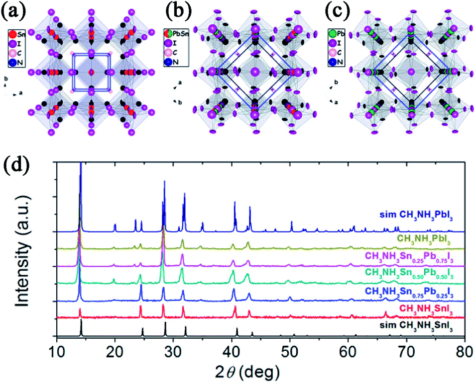 | ||
| Fig. 18 Crystal structure (a–c) and X-ray diffraction pattern (d) of the MASn1−xPbxI3 solid solutions. Simulated X-ray diffraction patterns of the two end compositions of MAPbI3 and MASnI3 are also shown in (d). Reprinted with permission.199 | ||
While the good semiconducting behaviour has been observed in the Pb/Sn alloy perovskite-based device, completely lead-free organic–inorganic tin halide perovskites have not exhibited inspiring photovoltaic performance, and have always yielded a relatively low fill factor (<60%), which is mainly because of the more significant self-doping in the Sn perovskites. So far, devices based on the different lead-free perovskites MASnI3 (ref. 199 and 201) (FTO/bl-TiO2/mp-TiO2/MASnI3/spiro-OMeTAD/Au), MASnI3−xBrx(ref. 202) (FTO/bl-TiO2/mp-TiO2/MASnI3−xBrx/spiro-OMeTAD/Au), MASnI3−xClx (ref. 200) (ITO/PEDOT:PSS/MASnI3−xClx/PC60BM/C60-bis/Ag) have yielded PCEs of 6.4%, 5.73%, and 0.04%, respectively.
7. Conclusions and prospects
In this review, we summarize and discuss recent developments in organometal halide perovskite-based all-solid-state solar cells. With extensive research and accumulated understanding, the unique physical and optoelectronic properties of organometal halide perovskites have been explored and elucidated. The organometal halide perovskites can not only act as light absorbers but also work efficiently in various device architectures going from a dye sensitized concept due to the bipolar transport of both holes and electrons.For the core part of ABX3 perovskites (a) reasonable structure engineering based on A (e.g. MA and FA), B (e.g. Pb and Sn), and/or X (e.g. Cl, Br and I) can effectively modify the resultant optical band gaps, the HOMO/LUMO energy levels as well as the charge diffusion length, which finally affect the resultant photovoltaic performance. For example, long electron–hole diffusion lengths exceeding 1 μm for the mixed halide perovskite of MAPbI3−xClx were measured, while it was only 100 nm for the triiodide perovskite of MAPbI3; (b) the morphology and crystals in perovskite films are not only related to the nature of materials, but also can be optimized by carefully modifying the deposition methods (e.g. solution-based deposition and vapor-based deposition) and/or controlling the device fabrication conditions (e.g. thermal annealing, additive treatment and solvent engineering); (c) since in perovskite layers, as well as for most ionic crystals, the coordination number for ions at the crystal surfaces is always lower than in the bulk material, disorderness with respect to energy (i.e., charge traps and structural defects) always exists at the perovskite surface and/or grain boundaries; thus a passivation technique (e.g. IPFB, Lewis base and PbI2) could be employed to lower carrier recombination rate and improve device performance.
For perovskite solar cells based on a porous structure (MMOPSC and MSSC), the porous scaffold can be conductive metal oxides including n-type TiO2 (17.01%, ITO/bl-TiO2/mp-TiO2/MAPbI3/spiro-OMeTAD/Au), ZnO (12%, FTO/bl-ZnO(Al)/mp-ZnO(Al)/MAPbI3/HTM/Ag) and p-type NiO (11.6%, ITO/bl-NiOx/mp-NiO/MAPbI3/PC60BM/BCP/Al); or insulating materials including Al2O3 (15.9%, FTO/bl-TiO2/mp-Al2O3/MAPbI3−xClx/spiro-OMeTAD/Ag), ZrO2 (10.8%, FTO/bl-TiO2/mp-ZrO2/MAPbI3/spiro-OMeTAD/Ag) and SiO2 (11.45%, FTO/bl-TiO2/mp-SiO2/MAPbI3−xClx/spiro-OMeTAD/Au). The contents in parentheses are the highest efficiencies and the corresponding device architectures based on different porous structures reported so far. At present, bl-TiO2/mp-TiO2/perovskite/HTM-based MMOPSC and bl-TiO2/mp-Al2O3/perovskite/HTM-based MSSC are the two most widely studied types of device architectures. Optimization of the following factors, (a) “scaffold” thickness and porosity modification, (b) interface/electrode engineering, (c) doping, and (d) HTM adjustment can effectively improve the device performance. Also, exploring on some new types of “scaffold” substances is still necessary (e.g. MO3,203 Zn2SnO4,204 SrTiO3 (ref. 205)). However, for fabricating these porous scaffolds as well as the thin blocking layer, especially employed in state-of-the-art perovskite solar cells, the process of sintering at high temperatures is always needed, which increases production cost and energy consumption, and also limits the possibility of fabricating large-area, flexible devices. Thus, in the future, developing low-temperature fabricated devices would be a promising direction and trend.
For PHJPSC, two configurations including a positive or inverted structure, in which a n-type (e.g. TiO2 and ZnO) or p-type conductor (e.g. PEDOT:PSS, NiO, CuSCN, graphene oxide and polythiophene) was coated on a conductive glass, have been widely studied with the highest PCEs of 19.3% (ITO/PEIE/bl-TiO2(Y)/MAPbI3−xClx/spiro-OMeTAD/Au) and 16.31% (ITO/PEDOT:PSS/MAPbI3/PC70BM/Ca/Al), respectively. Apart from the above-mentioned optimization methods of (b), (c) and (d) for MMOPSC and/or MSSC, the PHJ device performance is more dependent on the perovskite morphology, in particular the film thickness, roughness, and coverage. Also, due to the similar device architecture of the inverted planar perovskite solar cells (typically devices based on an ITO/PEDOT:PSS substrate) and the OPVs, some device engineering methods for OPVs can be used as a reference to this inverted perovskite device for further improving the device performance.
Although great success in the photovoltaic field has been achieved for organometal halide perovskites, the extremely high sensitivity of organometal halide perovskites to elevated temperature and moisture is still the main limiting factor for further practical application. Also, the low reproducibility, high deviation of the device performance and environmental pollution are problems exigent to be solved. Optimizing the perovskite material and structure of devices (e.g. large-area/flexible/durable/semitransparent/tandem device) will benefit its real application finally.26,206–214 We believe that, in the near future, the development of perovskite solar cells will open a new chapter on solving the problem of energy crisis.
Nomenclature
| 3-D | Three-dimensional |
| ALD | Atomic layer deposition |
| AZO | Al-doped mesoporous ZnO |
| BCP | Bathocuproine |
| BHJ | Bulk-heterojunction |
| Bphen | Bathophenanthroline |
| C60 | Fullerene |
| CBD | Chemical bath deposition |
| CE | Counter electrode |
| DIO | 1,8-Diiodooctane |
| DMF | N,N-Dimethylformamide |
| DMSO | Dimethylsulfoxide |
| DP | Deposition process |
| DSSC | Dye sensitized solar cell |
| DSVD | Dual source vacuum deposition |
| ETM | Electron-transporting material |
| FA | Formamidinium |
| FF | Fill factor |
| FG | Flaky graphite |
| FK102 | Tris(2-(1H-pyrazol-1-yl)pyridine)cobalt(III) tris(hexafluorophosphate) |
| FK209 | Tris(2-(1H-pyrazol-1-yl)-4-tert-butylpyridine)cobalt(III) tris(bis(trifluoromethylsulfonyl)imide) |
| FK269 | Bis(2,6-di(1H-pyrazol-1-yl)pyridine)cobalt(III) tris(bis(trifluoromethylsulfonyl)-imide) |
| FTO | Fluorine-doped tin oxide |
| GBL | γ-Butyrolactone |
| GO | Graphene oxide |
| HI | Hydroiodic acid |
| HMTA | Hexamethylenetetramine |
| HTM | Hole-transporting material |
| IC60BA | Indene–C60 bisadduct |
| IPCE | Incident photon-to-electron conversion efficiency |
| IPFB | Iodopentafluorobenzene |
| IQE | Internal quantum efficiency |
| ITO | Indium tin oxide |
| J sc | Short-circuit current density |
| LiTFSI | Bis(trifluoromethane)sulfonimide lithium salt |
| MMOPSC | Mesoporous metal oxide perovskite solar cell |
| MSSC | Meso-superstructured solar cell |
| NRA | Nanorod array |
| OPV | Organic photovoltaic cell |
| OSPD | One step precursor deposition |
| PA | Phenylamine |
| PC60BM | [6,6]-Phenyl C61-butyric acid methyl ester |
| PC70BM | [6,6]-Phenyl C71-butyric acid methyl ester |
| PCE | Power conversion efficiency |
| PDMS | Polydimethylsiloxane |
| PECVD | Plasma-enhanced chemical vapor deposition |
| PEIE | Polyethyleneimine ethoxylated |
| PET | Polyethylene terephthalate |
| PFI | Perfluorinated ionomer |
| PHJ | Planar heterojunction |
| PHJPSC | Planar heterojunction perovskite solar cell |
| PL | Perovskite layer |
| PMMA | Poly(methyl methacrylate) |
| Poly-TPD | Poly(N,N′-bis(4-butylphenyl)-N,N′-bis(phenyl)benzidine) |
| PT | Polythiophene |
| PTAA | Poly(triarylamine) |
| QDSC | Quantum dot solar cell |
| R s | Series resistance |
| R sh | Shunt resistance |
| SCD | Spray-coating deposition |
| SDP | Sequential deposition process |
| SG | Spheroidal graphite |
| Spiro-OMeTAD or spiro | 2′,7,7′-Tetrakis(N,N-di-p-methoxyphenylamine)-9,9′-spirobifluorene |
| ss-DSSCs | Solid-state dye-sensitized solar cells |
| SVD | Sequential vapour deposition |
| SWNTs | Single-walled carbon nanotubes |
| TAA | Triarylamine |
| TBP | 4-tert-Butylpyridine |
| TPA | Triphenylamine |
| TSSD | Two step spin-coating deposition |
| VASP | Vapor assisted solution process |
| V oc | Open-circuit voltage |
Notes and references
- http://news.sciencemag.org/breakthrough-of-the-year-2013 .
- http://www.nature.com/news/365-days-nature-s-10-1.14367 .
- P. V. Kamat, J. Am. Chem. Soc., 2014, 136, 3713 CrossRef CAS PubMed.
- Z. Cheng and J. Lin, CrystEngComm, 2010, 12, 2646 RSC.
- C. Li, X. Lu, W. Ding, L. Feng, Y. Gao and Z. Guo, Acta Crystallogr., Sect. B: Struct. Sci., 2008, 64, 702 CrossRef CAS PubMed.
- M. A. Green, A. Ho-Baillie and H. J. Snaith, Nat. Photonics, 2014, 8, 506 CrossRef CAS.
- I. Borriello, G. Cantele and D. Ninno, Phys. Rev. B: Condens. Matter Mater. Phys., 2008, 77, 235214 CrossRef.
- B. O'Regan and M. Grätzel, Nature, 1991, 353, 737 CrossRef.
- A. Yella, H. W. Lee, H. N. Tsao, C. Yi, A. K. Chandiran, M. K. Nazeeruddin, E. W. Diau, C. Y. Yeh, S. M. Zakeeruddin and M. Grätzel, Science, 2011, 334, 629 CrossRef CAS PubMed.
- U. Bach, D. Lupo, P. Comte, J. E. Moser, F. Weissörtel, J. Salbeck, H. Spreitzer and M. Grätzel, Nature, 1998, 395, 583 CrossRef CAS PubMed.
- J. Burschka, A. Dualeh, F. Kessler, E. Baranoff, N. L. Cevey-Ha, C. Yi, M. K. Nazeeruddin and M. Grätzel, J. Am. Chem. Soc., 2011, 133, 18042 CrossRef CAS PubMed.
- H. S. Kim, C. R. Lee, J. H. Im, K. B. Lee, T. Moehl, A. Marchioro, S. J. Moon, R. Humphry-Baker, J. H. Yum, J. E. Moser, M. Grätzel and N. G. Park, Sci. Rep., 2012, 2, 591 Search PubMed.
- M. M. Lee, J. Teuscher, T. Miyasaka, T. N. Murakami and H. J. Snaith, Science, 2012, 338, 643 CrossRef CAS PubMed.
- L. Etgar, P. Gao, Z. Xue, Q. Peng, A. K. Chandiran, B. Liu, M. K. Nazeeruddin and M. Grätzel, J. Am. Chem. Soc., 2012, 134, 17396 CrossRef CAS PubMed.
- A. Kojima, K. Teshima, Y. Shirai and T. Miyasaka, J. Am. Chem. Soc., 2009, 131, 6050 CrossRef CAS PubMed.
- J. H. Im, C. R. Lee, J. W. Lee, S. W. Park and N. G. Park, Nanoscale, 2011, 3, 4088 RSC.
- J. H. Im, J. Chung, S. J. Kim and N. G. Park, Nanoscale Res. Lett., 2012, 7, 353 CrossRef PubMed.
- J. Burschka, N. Pellet, S. J. Moon, R. Humphry-Baker, P. Gao, M. K. Nazeeruddin and M. Grätzel, Nature, 2013, 499, 316 CrossRef CAS PubMed.
- M. Liu, M. B. Johnston and H. J. Snaith, Nature, 2013, 501, 395 CrossRef CAS PubMed.
- J. H. Heo, S. H. Im, J. H. Noh, T. N. Mandal, C.-S. Lim, J. A. Chang, Y. H. Lee, H.-j. Kim, A. Sarkar, M. K. Nazeeruddin, M. Grätzel and S. I. Seok, Nat. Photonics, 2013, 7, 486 CrossRef CAS.
- J. H. Im, I. H. Jang, N. Pellet, M. Grätzel and N. G. Park, Nat. Nanotechnol., 2014, 9, 927 CrossRef CAS PubMed.
- K. Wojciechowski, M. Saliba, T. Leijtens, A. Abate and H. J. Snaith, Energy Environ. Sci., 2014, 7, 1142 CAS.
- H. Zhou, Q. Chen, G. Li, S. Luo, T. B. Song, H. S. Duan, Z. Hong, J. You, Y. Liu and Y. Yang, Science, 2014, 345, 542 CrossRef CAS PubMed.
- N. J. Jeon, J. H. Noh, Y. C. Kim, W. S. Yang, S. Ryu and S. I. Seok, Nat. Mater., 2014, 13, 897 CrossRef CAS PubMed.
- H. B. Kim, H. Choi, J. Jeong, S. Kim, B. Walker, S. Song and J. Y. Kim, Nanoscale, 2014, 6, 6679 RSC.
- J. Seo, S. Park, Y. Chan Kim, N. J. Jeon, J. H. Noh, S. C. Yoon and S. I. Seok, Energy Environ. Sci., 2014, 7, 2642 CAS.
- M. Xiao, F. Huang, W. Huang, Y. Dkhissi, Y. Zhu, J. Etheridge, A. Gray-Weale, U. Bach, Y. B. Cheng and L. Spiccia, Angew. Chem., Int. Ed., 2014, 53, 9898 CrossRef CAS PubMed.
- S. Paek, N. Cho, H. Choi, H. Jeong, J. S. Lim, J.-Y. Hwang, J. K. Lee and J. Ko, J. Phys. Chem. C, 2014, 118, 25899 CAS.
- J. W. Jung, S. T. Williams and A. K. Y. Jen, RSC Adv., 2014, 4, 62971 RSC.
- R. Kang, J.-E. Kim, J.-S. Yeo, S. Lee, Y.-J. Jeon and D.-Y. Kim, J. Phys. Chem. C, 2014, 118, 26513 CAS.
- G. E. Eperon, V. M. Burlakov, P. Docampo, A. Goriely and H. J. Snaith, Adv. Funct. Mater., 2014, 24, 151 CrossRef CAS.
- H. L. Hsu, C. P. Chen, J. Y. Chang, Y. Y. Yu and Y. K. Shen, Nanoscale, 2014, 6, 10281 RSC.
- M. Saliba, K. W. Tan, H. Sai, D. T. Moore, T. Scott, W. Zhang, L. A. Estroff, U. Wiesner and H. J. Snaith, J. Phys. Chem. C, 2014, 118, 17171 CAS.
- A. Dualeh, N. Tétreault, T. Moehl, P. Gao, M. K. Nazeeruddin and M. Grätzel, Adv. Funct. Mater., 2014, 24, 3250 CrossRef CAS.
- P. W. Liang, C. Y. Liao, C. C. Chueh, F. Zuo, S. T. Williams, X. K. Xin, J. Lin and A. K. Jen, Adv. Mater., 2014, 26, 3748 CrossRef CAS PubMed.
- Y. Zhao and K. Zhu, J. Phys. Chem. C, 2014, 118, 9412 CAS.
- Y. Zhao and K. Zhu, J. Am. Chem. Soc., 2014, 136, 12241 CrossRef CAS PubMed.
- C. Zuo and L. Ding, Nanoscale, 2014, 6, 9935 RSC.
- D. B. M. Kangning Liang and T. P. Michael, Chem. Mater., 1998, 10, 403 CrossRef.
- Y. Ma, L. Zheng, Y.-H. Chung, S. Chu, L. Xiao, Z. Chen, S. Wang, B. Qu, Q. Gong, Z. Wu and X. Hou, Chem. Commun., 2014, 50, 12458 RSC.
- Y. Wu, A. Islam, X. Yang, C. Qin, J. Liu, K. Zhang, W. Peng and L. Han, Energy Environ. Sci., 2014, 7, 2934 CAS.
- J. Shi, Y. Luo, H. Wei, J. Luo, J. Dong, S. Lv, J. Xiao, Y. Xu, L. Zhu, X. Xu, H. Wu, D. Li and Q. Meng, ACS Appl. Mater. Interfaces, 2014, 6, 9711 CAS.
- P. Docampo, F. C. Hanusch, N. Giesbrecht, P. Angloher, A. Ivanova and T. Bein, APL Mater., 2014, 2, 081508 CrossRef PubMed.
- L. Zheng, Y. Ma, S. Chu, S. Wang, B. Qu, L. Xiao, Z. Chen, Q. Gong, Z. Wu and X. Hou, Nanoscale, 2014, 6, 8171 RSC.
- D. H. Cao, C. C. Stoumpos, C. D. Malliakas, M. J. Katz, O. K. Farha, J. T. Hupp and M. G. Kanatzidis, APL Mater., 2014, 2, 091101 CrossRef PubMed.
- D. Bi, S.-J. Moon, L. Häggman, G. Boschloo, L. Yang, E. M. J. Johansson, M. K. Nazeeruddin, M. Grätzel and A. Hagfeldt, RSC Adv., 2013, 3, 18762 RSC.
- D. Liu and T. L. Kelly, Nat. Photonics, 2013, 8, 133 CrossRef.
- Q. Chen, H. Zhou, Z. Hong, S. Luo, H. S. Duan, H. H. Wang, Y. Liu, G. Li and Y. Yang, J. Am. Chem. Soc., 2014, 136, 622 CrossRef CAS PubMed.
- Z. Xiao, C. Bi, Y. Shao, Q. Dong, Q. Wang, Y. Yuan, C. Wang, Y. Gao and J. Huang, Energy Environ. Sci., 2014, 7, 2619 CAS.
- C.-H. Chiang, Z.-L. Tseng and C.-G. Wu, J. Mater. Chem. A, 2014, 2, 15897 CAS.
- J.-H. Im, H.-S. Kim and N.-G. Park, APL Mater., 2014, 2, 081510 CrossRef PubMed.
- A. T. Barrows, A. J. Pearson, C. K. Kwak, A. D. F. Dunbar, A. R. Buckley and D. G. Lidzey, Energy Environ. Sci., 2014, 7, 2944 CAS.
- D. T. Moore, H. Sai, K. Wee Tan, L. A. Estroff and U. Wiesner, APL Mater., 2014, 2, 081802 CrossRef PubMed.
- B.-E. Cohen, S. Gamliel and L. Etgar, APL Mater., 2014, 2, 081502 CrossRef PubMed.
- H. Hu, D. Wang, Y. Zhou, J. Zhang, S. Lv, S. Pang, X. Chen, Z. Liu, N. P. Padture and G. Cui, RSC Adv., 2014, 4, 28964 RSC.
- C. W. Chen, H. W. Kang, S. Y. Hsiao, P. F. Yang, K. M. Chiang and H. W. Lin, Adv. Mater., 2014, 26, 6647 CrossRef CAS PubMed.
- Q. Chen, H. Zhou, T. B. Song, S. Luo, Z. Hong, H. S. Duan, L. Dou, Y. Liu and Y. Yang, Nano Lett., 2014, 14, 4158 CrossRef CAS PubMed.
- T. Supasai, N. Rujisamphan, K. Ullrich, A. Chemseddine and T. Dittrich, Appl. Phys. Lett., 2013, 103, 183906 CrossRef PubMed.
- L. Wang, C. McCleese, A. Kovalsky, Y. Zhao and C. Burda, J. Am. Chem. Soc., 2014, 136, 12205 CrossRef CAS PubMed.
- N. J. Jeon, H. G. Lee, Y. C. Kim, J. Seo, J. H. Noh, J. Lee and S. I. Seok, J. Am. Chem. Soc., 2014, 136, 7837 CrossRef CAS PubMed.
- Y. Bai, I. Mora-Sero, F. De Angelis, J. Bisquert and P. Wang, Chem. Rev., 2014, 114, 10095 CrossRef CAS PubMed.
- G. Murugadoss, G. Mizuta, S. Tanaka, H. Nishino, T. Umeyama, H. Imahori and S. Ito, APL Mater., 2014, 2, 081511 CrossRef PubMed.
- B. Conings, L. Baeten, T. Jacobs, R. Dera, J. D'Haen, J. Manca and H. G. Boyen, APL Mater., 2014, 2, 081505 CrossRef PubMed.
- B. Conings, L. Baeten, C. De Dobbelaere, J. D'Haen, J. Manca and H. G. Boyen, Adv. Mater., 2014, 26, 2041 CrossRef CAS PubMed.
- W. Liu and Y. Zhang, J. Mater. Chem. A, 2014, 2, 10244 CAS.
- A. Yella, L. P. Heiniger, P. Gao, M. K. Nazeeruddin and M. Grätzel, Nano Lett., 2014, 14, 2591 CrossRef CAS PubMed.
- J. M. Ball, M. M. Lee, A. Hey and H. J. Snaith, Energy Environ. Sci., 2013, 6, 1739 CAS.
- Y. Wu, X. Yang, H. Chen, K. Zhang, C. Qin, J. Liu, W. Peng, A. Islam, E. Bi, F. Ye, M. Yin, P. Zhang and L. Han, Appl. Phys. Express, 2014, 7, 052301 CrossRef.
- A. K. Chandiran, A. Yella, M. T. Mayer, P. Gao, M. K. Nazeeruddin and M. Grätzel, Adv. Mater., 2014, 26, 4309 CrossRef CAS PubMed.
- P. Qin, A. L. Domanski, A. K. Chandiran, R. Berger, H. J. Butt, M. I. Dar, T. Moehl, N. Tetreault, P. Gao, S. Ahmad, M. K. Nazeeruddin and M. Grätzel, Nanoscale, 2014, 6, 1508 RSC.
- J. Xia, N. Masaki, K. Jiang and S. Yanagida, J. Phys. Chem. B, 2006, 110, 25222 CrossRef CAS PubMed.
- W. Ke, G. Fang, J. Wang, P. Qin, H. Tao, H. Lei, Q. Liu, X. Dai and X. Zhao, ACS Appl. Mater. Interfaces, 2014, 6, 15959 CAS.
- J. J. Choi, X. Yang, Z. M. Norman, S. J. Billinge and J. S. Owen, Nano Lett., 2014, 14, 127 CrossRef CAS PubMed.
- E. Edri, S. Kirmayer, A. Henning, S. Mukhopadhyay, K. Gartsman, Y. Rosenwaks, G. Hodes and D. Cahen, Nano Lett., 2014, 14, 1000 CrossRef CAS PubMed.
- Q. Shen, Y. Ogomi, J. Chang, S. Tsukamoto, K. Kukihara, T. Oshima, N. Osada, K. Yoshino, K. Katayama, T. Toyoda and S. Hayase, Phys. Chem. Chem. Phys., 2014, 16, 19984 RSC.
- Y. Zhao, A. M. Nardes and K. Zhu, Faraday Discuss., 2014 10.1039/c4fd00128a.
- R. Lindblad, D. Bi, B.-w. Park, J. Oscarsson, M. Gorgoi, H. Siegbahn, M. Odelius, E. M. J. Johansson and H. Rensmo, J. Phys. Chem. Lett., 2014, 5, 648 CrossRef CAS.
- J. W. Lee, T. Y. Lee, P. J. Yoo, M. Grätzel, S. Mhaisalkar and N. G. Park, J. Mater. Chem. A, 2014, 2, 9251 CAS.
- M. I. Dar, F. J. Ramos, Z. Xue, B. Liu, S. Ahmad, S. A. Shivashankar, M. K. Nazeeruddin and M. Grätzel, Chem. Mater., 2014, 26, 4675 CrossRef CAS.
- Y. Rong, Z. Ku, A. Mei, T. Liu, M. Xu, S. Ko, X. Li and H. Han, J. Phys. Chem. Lett., 2014, 5, 2160 CrossRef CAS.
- H. S. Kim, J. W. Lee, N. Yantara, P. P. Boix, S. A. Kulkarni, S. Mhaisalkar, M. Grätzel and N. G. Park, Nano Lett., 2013, 13, 2412 CrossRef CAS PubMed.
- K. Manseki, T. Ikeya, A. Tamura, T. Ban, T. Sugiura and T. Yoshida, RSC Adv., 2014, 4, 9652 RSC.
- J. Qiu, Y. Qiu, K. Yan, M. Zhong, C. Mu, H. Yan and S. Yang, Nanoscale, 2013, 5, 3245 RSC.
- H. Chen, Z. Wei, K. Yan, Y. Yi, J. Wang and S. Yang, Faraday Discuss., 2014 10.1039/c4fd00155a.
- M. Yang, R. Guo, K. Kadel, Y. Liu, K. O'Shea, R. Bone, X. Wang, J. He and W. Li, J. Mater. Chem. A, 2014, 2, 19616 CAS.
- X. Gao, J. Li, J. Baker, Y. Hou, D. Guan, J. Chen and C. Yuan, Chem. Commun., 2014, 50, 6368 RSC.
- Y. M. Xiao, G. Y. Han, Y. P. Li, M. Y. Li and J. H. Wu, J. Mater. Chem. A, 2014, 2, 16856 CAS.
- S. Dharani, H. K. Mulmudi, N. Yantara, P. T. Thu Trang, N. G. Park, M. Graetzel, S. Mhaisalkar, N. Mathews and P. P. Boix, Nanoscale, 2014, 6, 1675 RSC.
- Q. Jiang, X. Sheng, Y. Li, X. Feng and T. Xu, Chem. Commun., 2014, 50, 14720 RSC.
- E. J. Crossland, N. Noel, V. Sivaram, T. Leijtens, J. A. Alexander-Webber and H. J. Snaith, Nature, 2013, 495, 215 CrossRef CAS PubMed.
- G. S. Han, S. Lee, J. H. Noh, H. S. Chung, J. H. Park, B. S. Swain, J. H. Im, N. G. Park and H. S. Jung, Nanoscale, 2014, 6, 6127 RSC.
- Q. Zhang, C. S. Dandeneau, X. Zhou and G. Cao, Adv. Mater., 2009, 21, 4087 CrossRef CAS.
- J. A. Anta, E. Guillén and R. Tena-Zaera, J. Phys. Chem. C, 2012, 116, 11413 CAS.
- D. Bi, G. Boschloo, S. Schwarzmuller, L. Yang, E. M. Johansson and A. Hagfeldt, Nanoscale, 2013, 5, 11686 RSC.
- D. Y. Son, J. H. Im, H. S. Kim and N. G. Park, J. Phys. Chem. C, 2014, 118, 16567 CAS.
- M. H. Kumar, N. Yantara, S. Dharani, M. Graetzel, S. Mhaisalkar, P. P. Boix and N. Mathews, Chem. Commun., 2013, 49, 11089 RSC.
- F. J. Ramos, M. C. Lopez-Santos, E. Guillen, M. K. Nazeeruddin, M. Grätzel, A. R. Gonzalez-Elipe and S. Ahmad, ChemPhysChem, 2014, 15, 1148 CrossRef CAS PubMed.
- K. Mahmood, B. S. Swain and H. S. Jung, Nanoscale, 2014, 6, 9127 RSC.
- K. Mahmood, R. Munir, B. S. Swain, G.-S. Han, B.-J. Kim and H. S. Jung, RSC Adv., 2014, 4, 9072 RSC.
- J. Dong, Y. Zhao, J. Shi, H. Wei, J. Xiao, X. Xu, J. Luo, J. Xu, D. Li, Y. Luo and Q. Meng, Chem. Commun., 2014, 50, 13381 RSC.
- K. C. Wang, J. Y. Jeng, P. S. Shen, Y. C. Chang, E. W. G. Diau, C. H. Tsai, T. Y. Chao, H. C. Hsu, P. Y. Lin, P. Chen, T. F. Guo and T. C. Wen, Sci. Rep., 2014, 4, 4756 Search PubMed.
- J.-Y. Jeng, K.-C. Chen, T.-Y. Chiang, P.-Y. Lin, T.-D. Tsai, Y.-C. Chang, T.-F. Guo, P. Chen, T.-C. Wen and Y.-J. Hsu, Adv. Mater., 2014, 26, 4107 CrossRef CAS PubMed.
- L. Hu, J. Peng, W. Wang, Z. Xia, J. Yuan, J. Lu, X. Huang, W. Ma, H. Song, W. Chen, Y.-B. Cheng and J. Tang, ACS Photonics, 2014, 1, 547 CrossRef CAS.
- K. C. Wang, P. S. Shen, M. H. Li, S. Chen, M. W. Lin, P. Chen and T. F. Guo, ACS Appl. Mater. Interfaces, 2014, 6, 11851 CAS.
- E. Edri, S. Kirmayer, D. Cahen and G. Hodes, J. Phys. Chem. Lett., 2013, 4, 897 CrossRef CAS.
- W. Zhang, M. Saliba, S. D. Stranks, Y. Sun, X. Shi, U. Wiesner and H. J. Snaith, Nano Lett., 2013, 13, 4505 CrossRef CAS PubMed.
- M. J. Carnie, C. Charbonneau, M. L. Davies, J. Troughton, T. M. Watson, K. Wojciechowski, H. Snaith and D. A. Worsley, Chem. Commun., 2013, 49, 7893 RSC.
- A. Abate, M. Saliba, D. J. Hollman, S. D. Stranks, K. Wojciechowski, R. Avolio, G. Grancini, A. Petrozza and H. J. Snaith, Nano Lett., 2014, 14, 3247 CrossRef CAS PubMed.
- S. K. Pathak, A. Abate, P. Ruckdeschel, B. Roose, K. C. Godel, Y. Vaynzof, A. Santhala, S. I. Watanabe, D. J. Hollman, N. Noel, A. Sepe, U. Wiesner, R. Friend, H. J. Snaith and U. Steiner, Adv. Funct. Mater., 2014, 24, 6046 CrossRef CAS.
- S. N. Habisreutinger, T. Leijtens, G. E. Eperon, S. D. Stranks, R. J. Nicholas and H. J. Snaith, Nano Lett., 2014, 14, 5561 CrossRef CAS PubMed.
- J. T. Wang, J. M. Ball, E. M. Barea, A. Abate, J. A. Alexander-Webber, J. Huang, M. Saliba, I. Mora-Sero, J. Bisquert, H. J. Snaith and R. J. Nicholas, Nano Lett., 2014, 14, 724 CrossRef CAS PubMed.
- X. Dong, H. Hu, B. Lin, J. Ding and N. Yuan, Chem. Commun., 2014, 50, 14405 RSC.
- H. S. Kim, I. Mora-Sero, V. Gonzalez-Pedro, F. Fabregat-Santiago, E. J. Juarez-Perez, N. G. Park and J. Bisquert, Nat. Commun., 2013, 4, 2242 Search PubMed.
- S. H. Hwang, J. Roh, J. Lee, J. Ryu, J. Yun and J. Jang, J. Mater. Chem. A, 2014, 2, 16429 CAS.
- S. D. Stranks, G. E. Eperon, G. Grancini, C. Menelaou, M. J. Alcocer, T. Leijtens, L. M. Herz, A. Petrozza and H. J. Snaith, Science, 2013, 342, 341 CrossRef CAS PubMed.
- G. Xing, N. Mathews, S. Sun, S. S. Lim, Y. M. Lam, M. Grätzel, S. Mhaisalkar and T. C. Sum, Science, 2013, 342, 344 CrossRef CAS PubMed.
- P. Docampo, F. C. Hanusch, S. D. Stranks, M. Döblinger, J. M. Feckl, M. Ehrensperger, N. K. Minar, M. B. Johnston, H. J. Snaith and T. Bein, Adv. Energy Mater., 2014, 4 DOI:10.1002/aenm.201400355.
- J. Kim, G. Kim, T. K. Kim, S. Kwon, H. Back, J. Lee, S. H. Lee, H. Kang and K. Lee, J. Mater. Chem. A, 2014, 2, 17291 CAS.
- L. Liang, Z. Huang, L. Cai, W. Chen, B. Wang, K. Chen, H. Bai, Q. Tian and B. Fan, ACS Appl. Mater. Interfaces, 2014, 6, 20585 CAS.
- L. Zheng, Y. H. Chung, Y. Ma, L. Zhang, L. Xiao, Z. Chen, S. Wang, B. Qu and Q. Gong, Chem. Commun., 2014, 50, 11196 RSC.
- S. Chavhan, O. Miguel, H. J. Grande, V. Gonzalez-Pedro, R. S. Sanchez, E. M. Barea, I. Mora-Sero and R. Tena-Zaera, J. Mater. Chem. A, 2014, 2, 12754 CAS.
- N. K. Noel, A. Abate, S. D. Stranks, E. S. Parrott, V. M. Burlakov, A. Goriely and H. J. Snaith, ACS Nano, 2014, 8, 9815 CrossRef CAS PubMed.
- J. Y. Jeng, Y. F. Chiang, M. H. Lee, S. R. Peng, T. F. Guo, P. Chen and T. C. Wen, Adv. Mater., 2013, 25, 3727 CrossRef CAS PubMed.
- S. Sun, T. Salim, N. Mathews, M. Duchamp, C. Boothroyd, G. Xing, T. C. Sum and Y. M. Lam, Energy Environ. Sci., 2014, 7, 399 CAS.
- P. Docampo, J. M. Ball, M. Darwich, G. E. Eperon and H. J. Snaith, Nat. Commun., 2013, 4, 2761 Search PubMed.
- O. Malinkiewicz, A. Yella, Y. H. Lee, G. M. Espallargas, M. Graetzel, M. K. Nazeeruddin and H. J. Bolink, Nat. Photonics, 2013, 8, 128 CrossRef.
- O. Malinkiewicz, C. Roldán-Carmona, A. Soriano, E. Bandiello, L. Camacho, M. K. Nazeeruddin and H. J. Bolink, Adv. Energy Mater., 2014, 4 DOI:10.1002/aenm.201400345.
- J. You, Z. Hong, Y. M. Yang, Q. Chen, M. Cai, T. B. Song, C. C. Chen, S. Lu, Y. Liu, H. Zhou and Y. Yang, ACS Nano, 2014, 8, 1674 CrossRef CAS PubMed.
- K.-G. Lim, H.-B. Kim, J. Jeong, H. Kim, J. Y. Kim and T.-W. Lee, Adv. Mater., 2014, 26, 6461 CrossRef CAS PubMed.
- Q. Wang, Y. C. Shao, Q. F. Dong, Z. G. Xiao, Y. B. Yuan and J. S. Huang, Energy Environ. Sci., 2014, 7, 2359 CAS.
- Z. Xiao, Q. Dong, C. Bi, Y. Shao, Y. Yuan and J. Huang, Adv. Mater., 2014, 26, 6503 CrossRef CAS PubMed.
- A. S. Subbiah, A. Halder, S. Ghosh, N. Mahuli, G. Hodes and S. K. Sarkar, J. Phys. Chem. Lett., 2014, 5, 1748 CrossRef CAS.
- Z. Zhu, Y. Bai, T. Zhang, Z. Liu, X. Long, Z. Wei, Z. Wang, L. Zhang, J. Wang, F. Yan and S. Yang, Angew. Chem., Int. Ed., 2014, 53, 12571 CAS.
- Z. Wu, S. Bai, J. Xiang, Z. Yuan, Y. Yang, W. Cui, X. Gao, Z. Liu, Y. Jin and B. Sun, Nanoscale, 2014, 6, 10505 RSC.
- W. Yan, Y. Li, W. Sun, H. Peng, S. Ye, Z. Liu, Z. Bian and C. Huang, RSC Adv., 2014, 4, 33039 RSC.
- D. Bi, L. Yang, G. Boschloo, A. Hagfeldt and E. M. J. Johansson, J. Phys. Chem. Lett., 2013, 4, 1532 CrossRef CAS.
- N. J. Jeon, J. Lee, J. H. Noh, M. K. Nazeeruddin, M. Grätzel and S. I. Seok, J. Am. Chem. Soc., 2013, 135, 19087 CrossRef CAS PubMed.
- H. Li, K. Fu, A. Hagfeldt, M. Grätzel, S. G. Mhaisalkar and A. C. Grimsdale, Angew. Chem., Int. Ed., 2014, 53, 4085 CrossRef CAS PubMed.
- T. Krishnamoorthy, F. Kunwu, P. P. Boix, H. Li, T. M. Koh, W. L. Leong, S. Powar, A. Grimsdale, M. Grätzel, N. Mathews and S. G. Mhaisalkar, J. Mater. Chem. A, 2014, 2, 6305 CAS.
- A. Krishna, D. Sabba, H. R. Li, J. Yin, P. P. Boix, C. Soci, S. G. Mhaisalkar and A. C. Grimsdale, Chem. Sci., 2014, 5, 2702 RSC.
- H. Choi, S. Paek, N. Lim, Y. H. Lee, M. K. Nazeeruddin and J. Ko, Chem.–Eur. J., 2014, 20, 10894 CrossRef CAS PubMed.
- Y. Song, S. Lv, X. Liu, X. Li, S. Wang, H. Wei, D. Li, Y. Xiao and Q. Meng, Chem. Commun., 2014, 50, 15239 RSC.
- B. Xu, E. Sheibani, P. Liu, J. Zhang, H. Tian, N. Vlachopoulos, G. Boschloo, L. Kloo, A. Hagfeldt and L. Sun, Adv. Mater., 2014, 26, 6629 CrossRef CAS PubMed.
- S. D. Sung, M. S. Kang, I. T. Choi, H. M. Kim, H. Kim, M. Hong, H. K. Kim and W. I. Lee, Chem. Commun., 2014, 50, 14161 RSC.
- J. Wang, S. Wang, X. Li, L. Zhu, Q. Meng, Y. Xiao and D. Li, Chem. Commun., 2014, 50, 5829 RSC.
- S. Lv, L. Han, J. Xiao, L. Zhu, J. Shi, H. Wei, Y. Xu, J. Dong, X. Xu, D. Li, S. Wang, Y. Luo, Q. Meng and X. Li, Chem. Commun., 2014, 50, 6931 RSC.
- J. Xiao, L. Han, L. Zhu, S. Lv, J. Shi, H. Wei, Y. Xu, J. Dong, X. Xu, Y. Xiao, D. Li, S. Wang, Y. Luo, X. Li and Q. Meng, RSC Adv., 2014, 4, 32918 RSC.
- L. E. Polander, P. Pahner, M. Schwarze, M. Saalfrank, C. Koerner and K. Leo, APL Mater., 2014, 2, 081503 CrossRef PubMed.
- E. Edri, S. Kirmayer, M. Kulbak, G. Hodes and D. Cahen, J. Phys. Chem. Lett., 2014, 5, 429 CrossRef CAS.
- P. Qin, H. Kast, M. K. Nazeeruddin, S. M. Zakeeruddin, A. Mishra, P. Bäuerle and M. Grätzel, Energy Environ. Sci., 2014, 7, 2981 CAS.
- P. Qin, S. Paek, M. I. Dar, N. Pellet, J. Ko, M. Grätzel and M. K. Nazeeruddin, J. Am. Chem. Soc., 2014, 136, 8516 CrossRef CAS PubMed.
- J. Liu, Y. Wu, C. Qin, X. Yang, T. Yasuda, A. Islam, K. Zhang, W. Peng, W. Chen and L. Han, Energy Environ. Sci., 2014, 7, 2963 CAS.
- B. Cai, Y. Xing, Z. Yang, W.-H. Zhang and J. Qiu, Energy Environ. Sci., 2013, 6, 1480 CAS.
- F. Di Giacomo, S. Razza, F. Matteocci, A. D'Epifanio, S. Licoccia, T. M. Brown and A. Di Carlo, J. Power Sources, 2014, 251, 152 CrossRef CAS PubMed.
- Y. Guo, C. Liu, K. Lnoue, K. Harano, H. Tanaka and E. Nakamura, J. Mater. Chem. A, 2014, 2, 13827 CAS.
- J. H. Heo and S. H. Im, Phys. Status Solidi RRL, 2014, 8, 816 CrossRef CAS.
- M. Zhang, M. Lyu, H. Yu, J.-H. Yun, Q. Wang and L. Wang, Chem.–Eur. J., 2014, 21, 434 CrossRef PubMed.
- S. Ryu, J. H. Noh, N. J. Jeon, Y. C. Kim, S. Yang, J. W. Seo and S. I. Seok, Energy Environ. Sci., 2014, 7, 2614 CAS.
- Z. Zhu, Y. Bai, H. K. H. Lee, C. Mu, T. Zhang, L. Zhang, J. Wang, H. Yan, S. K. So and S. Yang, Adv. Funct. Mater., 2014, 24, 7357 CrossRef CAS.
- P. Qin, N. Tetreault, M. I. Dar, P. Gao, K. L. McCall, S. R. Rutter, S. D. Ogier, N. D. Forrest, J. S. Bissett, M. J. Simms, A. J. Page, R. Fisher, M. Grätzel and M. K. Nazeeruddin, Adv. Energy Mater., 2014 DOI:10.1002/aenm.201400980.
- Y. S. Kwon, J. Lim, H.-J. Yun, Y.-H. Kim and T. Park, Energy Environ. Sci., 2014, 7, 1454 CAS.
- J. W. Lee, S. Park, M. J. Ko, H. J. Son and N. G. Park, ChemPhysChem, 2014, 15, 2595 CrossRef CAS PubMed.
- A. Abrusci, S. D. Stranks, P. Docampo, H. L. Yip, A. K. Jen and H. J. Snaith, Nano Lett., 2013, 13, 3124 CrossRef CAS PubMed.
- J. A. Christians, R. C. Fung and P. V. Kamat, J. Am. Chem. Soc., 2014, 136, 758 CrossRef CAS PubMed.
- S. Ito, S. Tanaka, K. Manabe and H. Nishino, J. Phys. Chem. C, 2014, 118, 16995 CAS.
- S. Ito, S. Tanaka, H. Vahlman, H. Nishino, K. Manabe and P. Lund, ChemPhysChem, 2014, 15, 1194 CrossRef CAS PubMed.
- P. Qin, S. Tanaka, S. Ito, N. Tetreault, K. Manabe, H. Nishino, M. K. Nazeeruddin and M. Grätzel, Nat. Commun., 2014, 5, 3834 CAS.
- M. D. Irwin, D. B. Buchholz, A. W. Hains, R. P. H. Chang and T. J. Marks, Proc. Natl. Acad. Sci. U. S. A., 2008, 105, 2783 CrossRef CAS.
- K. X. Steirer, P. F. Ndione, N. E. Widjonarko, M. T. Lloyd, J. Meyer, E. L. Ratcliff, A. Kahn, N. R. Armstrong, C. J. Curtis, D. S. Ginley, J. J. Berry and D. C. Olson, Adv. Energy Mater., 2011, 1, 813 CrossRef CAS.
- W. A. Laban and L. Etgar, Energy Environ. Sci., 2013, 6, 3249 CAS.
- S. Aharon, S. Gamliel, B. E. Cohen and L. Etgar, Phys. Chem. Chem. Phys., 2014, 16, 10512 RSC.
- S. Aharon, B. El Cohen and L. Etgar, J. Phys. Chem. C, 2014, 118, 17160 CAS.
- J. J. Shi, W. Dong, Y. Z. Xu, C. H. Li, S. T. Lv, L. F. Zhu, J. Dong, Y. H. Luo, D. M. Li, Q. B. Meng and Q. Chen, Chin. Phys. Lett., 2013, 30, 128402 CrossRef.
- Y. Xu, J. Shi, S. Lv, L. Zhu, J. Dong, H. Wu, Y. Xiao, Y. Luo, S. Wang, D. Li, X. Li and Q. Meng, ACS Appl. Mater. Interfaces, 2014, 6, 5651 CAS.
- J. Shi, J. Dong, S. Lv, Y. Xu, L. Zhu, J. Xiao, X. Xu, H. Wu, D. Li, Y. Luo and Q. Meng, Appl. Phys. Lett., 2014, 104, 063901 CrossRef PubMed.
- Y. M. Xiao, G. Y. Han, Y. P. Li, M. Y. Li, Y. Z. Chang and J. H. Wu, J. Mater. Chem. A, 2014, 2, 16531 CAS.
- F. Hao, C. C. Stoumpos, Z. Liu, R. P. Chang and M. G. Kanatzidis, J. Am. Chem. Soc., 2014, 136, 16411 CrossRef CAS PubMed.
- Z. Ku, Y. Rong, M. Xu, T. Liu and H. Han, Sci. Rep., 2013, 3, 3132 Search PubMed.
- M. Xu, Y. Rong, Z. Ku, A. Mei, T. Liu, L. Zhang, X. Li and H. Han, J. Mater. Chem. A, 2014, 2, 8607 CAS.
- M. Hu, L. Liu, A. Mei, Y. Yang, T. Liu and H. Han, J. Mater. Chem. A, 2014, 2, 17115 CAS.
- A. Mei, X. Li, L. Liu, Z. Ku, T. Liu, Y. Rong, M. Xu, M. Hu, J. Chen, Y. Yang, M. Grätzel and H. Han, Science, 2014, 345, 295 CrossRef CAS PubMed.
- Z. Liu, M. Zhang, X. Xu, L. Bu, W. Zhang, W. Li, Z. Zhao, M. Wang, Y. B. Cheng and H. He, Dalton Trans., 2014 10.1039/c4dt02904f.
- F. Zhang, X. Yang, H. Wang, M. Cheng, J. Zhao and L. Sun, ACS Appl. Mater. Interfaces, 2014, 6, 16140 CAS.
- H. Zhou, Y. Shi, Q. Dong, H. Zhang, Y. Xing, K. Wang, Y. Du and T. Ma, J. Phys. Chem. Lett., 2014, 5, 3241 CrossRef CAS.
- Y. Yang, J. Xiao, H. Wei, L. Zhu, D. Li, Y. Luo, H. Wu and Q. Meng, RSC Adv., 2014, 4, 52825 RSC.
- Z. Wei, H. Chen, K. Yan and S. Yang, Angew. Chem., Int. Ed., 2014, 53, 13239 CrossRef CAS PubMed.
- N. Kitazawa, Y. Watanabe and Y. Nakamura, J. Mater. Sci., 2002, 37, 3585 CrossRef CAS.
- J. H. Noh, S. H. Im, J. H. Heo, T. N. Mandal and S. I. Seok, Nano Lett., 2013, 13, 1764 CAS.
- T. M. Koh, K. Fu, Y. Fang, S. Chen, T. C. Sum, N. Mathews, S. G. Mhaisalkar, P. P. Boix and T. Baikie, J. Phys. Chem. C, 2014, 118, 16458 CAS.
- S. Pang, H. Hu, J. Zhang, S. Lv, Y. Yu, F. Wei, T. Qin, H. Xu, Z. Liu and G. Cui, Chem. Mater., 2014, 26, 1485 CrossRef CAS.
- G. E. Eperon, S. D. Stranks, C. Menelaou, M. B. Johnston, L. M. Herz and H. J. Snaith, Energy Environ. Sci., 2014, 7, 982 CAS.
- C. C. Stoumpos, C. D. Malliakas and M. G. Kanatzidis, Inorg. Chem., 2013, 52, 9019 CrossRef CAS PubMed.
- J. W. Lee, D. J. Seol, A. N. Cho and N. G. Park, Adv. Mater., 2014, 26, 4991 CrossRef CAS PubMed.
- N. Pellet, P. Gao, G. Gregori, T. Y. Yang, M. K. Nazeeruddin, J. Maier and M. Grätzel, Angew. Chem., Int. Ed., 2014, 53, 3151 CrossRef CAS PubMed.
- S. Lv, S. Pang, Y. Zhou, N. P. Padture, H. Hu, L. Wang, X. Zhou, H. Zhu, L. Zhang, C. Huang and G. Cui, Phys. Chem. Chem. Phys., 2014, 16, 19206 RSC.
- F. C. Hanusch, E. Wiesenmayer, E. Mankel, A. Binek, P. Angloher, C. Fraunhofer, N. Giesbrecht, J. M. Feckl, W. Jaegermann, D. Johrendt, T. Bein and P. Docampo, J. Phys. Chem. Lett., 2014, 5, 2791 CrossRef CAS.
- C. Bernal and K. Yang, J. Phys. Chem. C, 2014, 118, 24383 CAS.
- Y. Ogomi, A. Morita, S. Tsukamoto, T. Saitho, N. Fujikawa, Q. Shen, T. Toyoda, K. Yoshino, S. S. Pandey, T. Ma and S. Hayase, J. Phys. Chem. Lett., 2014, 5, 1004 CrossRef CAS.
- F. Hao, C. C. Stoumpos, R. P. Chang and M. G. Kanatzidis, J. Am. Chem. Soc., 2014, 136, 8094 CrossRef CAS PubMed.
- F. Zuo, S. T. Williams, P. W. Liang, C. C. Chueh, C. Y. Liao and A. K. Jen, Adv. Mater., 2014, 26, 6454 CrossRef CAS PubMed.
- N. K. Noel, S. D. Stranks, A. Abate, C. Wehrenfennig, S. Guarnera, A.-A. Haghighirad, A. Sadhanala, G. E. Eperon, S. K. Pathak, M. B. Johnston, A. Petrozza, L. M. Herz and H. J. Snaith, Energy Environ. Sci., 2014, 7, 3061 CAS.
- F. Hao, C. C. Stoumpos, D. H. Cao, R. P. H. Chang and M. G. Kanatzidis, Nat. Photonics, 2014, 8, 489 CrossRef CAS.
- K. Mahmood, B. S. Swain, A. R. Kirmani and A. Amassian, J. Mater. Chem. A, 2015 10.1039/c4ta04883k.
- L. S. Oh, D. H. Kim, J. A. Lee, S. S. Shin, J.-W. Lee, I. J. Park, M. J. Ko, N.-G. Park, S. G. Pyo, K. S. Hong and J. Y. Kim, J. Phys. Chem. C, 2014, 118, 22991 CAS.
- A. Bera, K. Wu, A. Sheikh, E. Alarousu, O. F. Mohammed and T. Wu, J. Phys. Chem. C, 2014, 118, 28494 CAS.
- G. E. Eperon, V. M. Burlakov, A. Goriety and H. J. Snaith, ACS Nano, 2014, 8, 591 CrossRef CAS PubMed.
- P.-Y. Chen, J. Qi, M. T. Klug, X. Dang, P. T. Hammond and A. M. Belcher, Energy Environ. Sci., 2014, 7, 3659 CAS.
- E. Horvath, M. Spina, Z. Szekrenyes, K. Kamaras, R. Gaal, D. Gachet and L. Forro, Nano Lett., 2014, 14, 6761 CrossRef CAS PubMed.
- S. M. Kang, N. Ahn, J.-W. Lee, M. Choi and N.-G. Park, J. Mater. Chem. A, 2014, 2, 20017 CAS.
- B. J. Kim, D. H. Kim, Y.-Y. Lee, H.-W. Shin, G. S. Han, J. S. Hong, K. Mahmood, T. K. Ahn, Y.-C. Joo, K. S. Hong, N.-G. Park, S. Lee and H. S. Jung, Energy Environ. Sci., 2014 10.1039/c4ee02441a.
- F. Matteocci, S. Razza, F. Di Giacomo, S. Casaluci, G. Mincuzzi, T. M. Brown, A. D'Epifanio, S. Licoccia and A. Di Carlo, Phys. Chem. Chem. Phys., 2014, 16, 3918 RSC.
- L. Qiu, J. Deng, X. Lu, Z. Yang and H. Peng, Angew. Chem., Int. Ed., 2014, 53, 10425 CrossRef CAS PubMed.
- C. Roldán-Carmona, O. Malinkiewicz, R. Betancur, G. Longo, C. Momblona, F. Jaramillo, L. Camacho and H. J. Bolink, Energy Environ. Sci., 2014, 7, 2968 Search PubMed.
- C. Chen, S. Hsiao, C. Chen, H. Kang, Z. Huang and H. Lin, J. Mater. Chem. A 10.1039/c4ta05237d.
| This journal is © The Royal Society of Chemistry 2015 |