
Modulation of hybrid organic–perovskite photovoltaic performance by controlling the excited dynamics of fullerenes†
Chang-Zhi
Li
a,
Po-Wei
Liang
a,
Dana B.
Sulas
b,
Phu D.
Nguyen
b,
Xiaosong
Li
b,
David S.
Ginger
b,
Cody W.
Schlenker
b and
Alex K.-Y.
Jen
*ab
aDepartment of Materials Science and Engineering, University of Washington, Seattle, WA 98195, USA. E-mail: ajen@u.washington.edu
bDepartment of Chemistry, University of Washington, Seattle, WA 98195, USA
First published on 2nd April 2015
Abstract
We present a synergistic approach to modulate organic–perovskite interfaces and their photovoltaic behaviors by tuning the properties of n-contact fullerenes layered atop of perovskite. Fullerenes with excited charge transfer are found to not only suppress fullerene photoluminescence, but also enhance molecular polarization and transport capabilities. This results in optimized perovskite–fullerene contact.
Conceptual insightsRecent developments demonstrated that perovskite photovoltaics can be well built with an inorganic–organic p–i–n planar heterojunction architecture, in which organics interface with the perovskite. Across this heterointerface between two distinct material classes, efficient extraction of photogenerated charge carriers needs to be fulfilled in determining efficient device operation. One piece of absent chemical and physical pictures associated with these is how the organic functionalities control the properties of such a heterointerface. This report presents a synergistic approach to modulate organic–perovskite interfaces and their corresponding photovoltaic behaviors by tuning the properties of n-contact fullerenes layered atop of perovskite. The integrative chemistry, devices, computational and spectroscopic studies show that fullerenes with excited charge transfer (CT) characteristics compete with singlet exciton decay and counteract the excitonic nature associated with regular organic semiconductors. An important correlation is elucidated, which shows that the increase of excited CT probabilities between the fullerene and triphenylamine functionalities of n-layer organic contacts results in optimized interface and device operation of perovskite photovoltaics, with photocurrent enhancement and elimination of device hysteresis. This study provides a conceptually innovative model and identifies material knobs to uncover the fundamental factors of organic–inorganic hybrid electronics. |
Methyl ammonium lead halide perovskites have recently gained popularity as solution-processable materials for highly efficient photovoltaics (PVs), with power conversion efficiencies (PCEs) rising from 3.8% to over 20% within the last five years.1–5 State-of-the-art perovskite photovoltaics perform well with an inorganic–organic p–i–n planar heterojunction (PHJ) architecture, in which organic layers (p or n-layer) interface with the perovskite (i-layer) (Scheme 1).5–11 One intriguing, yet less explored, question is how the properties of the organic–perovskite heterointerface affect the operation of photovoltaics. Ideally, efficient device operation requires photo-generated charge carriers to be extracted from the perovskite into molecular orbitals of organic semiconductors with only minimal energy and carrier losses.12–14 Appropriate charge selective contacts are vital to realize this.15 Low charge carrier mobilities and carrier densities in organic semiconductors may limit efficient charge extraction at the perovskite/organic interface. For instance, commonly used electron extraction layers, such as non-polar PCBM,16 typically have mobilities around 10−2 cm2 V−1 s−1 in comparison to the organohalide lead perovskite, which exhibits a very high carrier mobility of ∼30 cm2 V−1 s−1 and photoconductivities up to 10−2 S cm−1.17–20 In addition, the search for new electron-selective contacts is also largely motivated by the desire to introduce mild processing materials for device fabrication.
 | ||
| Scheme 1 Schematic representation of the excited CT character of four chosen fullerene derivatives that are layered atop of CH3NH3PbI3−xClx perovskite planar heterojunction PVs. | ||
In this work, we present a synergistic approach to modulate organic–perovskite interfaces and their photovoltaic behaviours by tuning the properties of n-contact fullerenes layered atop of perovskite (Scheme 1). New fullerenes are functionalized with triphenylamine (TPA) moieties and used as n-layer contacts to CH3NH3PbI3−xClx perovskite for PHJ PVs. The resulting photovoltaic devices employing these fullerenes show correlations between increasing photocurrent and increasing electron-donating character of the TPA. The integrative computational and spectroscopic studies on these chosen materials suggest that the increase of CT probabilities between the fullerene and TPA competes with singlet exciton decay and counteracts the excitonic nature associated with regular organic semiconductors. Accordingly, fullerenes exhibiting CT characteristics simultaneously improve molecular polarization, carrier densities, and charge transport capabilities under light excitation, leading to improved photocurrent and performance of perovskite PVs when the perovskite layer is interfaced with these fullerenes.
Scheme 1 shows the molecular structures of the fullerenes we studied, PCBM, TPA–PCBM, BrTPA–PCBM and CNTPA–PCBM, respectively, where we replace the phenyl group of PC61BM with functional TPA moieties (ESI,† Fig. S1 and S2).21,22 The resulting fullerenes can be easily processed through common organic solvents, such as chloroform, toluene, chlorobenzene, and o-dichlorobenzene. TPA–PC61BM was previously demonstrated to improve the thermal stability of BHJ solar cells with P3HT due to its low crystallinity and good electron mobility.22 In the present study, we examine how the fine-tuning of TPA moieties affects the operation of fullerene–perovskite junctions and their photovoltaic behaviours. By increasing the electron-withdrawing abilities of the TPA substituents (H < Br ≪ CN), we effectively tune the donating strength of TPA moieties and regulate CT between TPA and the fullerene cage (i.e. electron localization on the fullerene and hole localization on the TPA). These changes result in the modulation of PV performance.
We first examine these modified fullerenes as n-layer contacts atop of the CH3NH3PbI3−xClx perovskite absorber, and we find ∼99% quenching of the perovskite photoluminescence intensity (Fig. S3, ESI†), suggesting effective charge transfer from the perovskite to the fullerene layer. We employ a planar heterojunction (PHJ) solar cell architecture to evaluate their photovoltaic performance in the configuration of ITO/PEDOT:PSS (∼30 nm)/perovskite (∼250 nm)/fullerene (∼55 nm)/bis-C60 (10 nm)/Ag (150 nm).6 The purpose of using relatively thin perovskite from the one-step process is to provide easier probing of the effect of fullerene functionalities on the photovoltaic behaviours of organic–perovskite PHJ solar cells. A bis-C60 interfacial layer is used to improve the interfacial contact between n-layer fullerenes and silver cathodes (please see the ESI† for a bis-C60 structure).23–25Fig. 1 and Table 1 summarize the current–voltage characteristics, external quantum efficiency (EQE), and overall perovskite device performance with the four different fullerene n-layers under 1 sun AM 1.5 simulated solar irradiation.
 | ||
| Fig. 1 (a) Current density–voltage curves by reverse and forward sweeping at a rate of 1 V s−1. (b) EQE spectra of the different fullerene based solar cells measured under AM 1.5G illumination at 100 mW cm−2. | ||
| PCE (%) | V OC/V | FF | J SC/mA cm−2 | |
|---|---|---|---|---|
| a The error bars represent the standard deviation of 25 devices. | ||||
| PCBM | 9.88 ± 0.37 | 0.90 ± 0.01 | 0.68 ± 0.02 | 15.70 ± 0.42 |
| TPA– | 10.87 ± 0.51 | 0.88 ± 0.02 | 0.69 ± 0.03 | 17.71 ± 0.54 |
| BrTPA– | 10.20 ± 0.38 | 0.89 ± 0.02 | 0.67 ± 0.05 | 17.18 ± 0.43 |
| CNTPA– | 5.60 ± 0.81 | 0.90 ± 0.02 | 0.48 ± 0.06 | 13.76 ± 0.37 |
The proof-of-concept device employing the TPA–PCBM contact layer exhibits a promising averaged PCE of 10.87 ± 0.51% with a much improved JSC of 17.71 ± 0.54 mA cm−2, which represents a ∼13% enhancement of JSC compared to that of the standard PC61BM device (JSC, 15.70 ± 0.42 mA cm−2 and PCE of 9.88 ± 0.37%). This notable current enhancement is consistent with the improved EQE over the entire spectral range shown in Fig. 1b. The TPA–PCBM based devices achieve a photon-to-electron conversion of ∼80% of external quantum efficiencies (EQE) in a broad range of spectra, which is comparable to that of state-of-the-art perovskite devices reported so far.26 A similar current enhancement for BrTPA–PCBM, with higher JSC and EQE as well as decent PCE of 10.20 ± 0.38% (VOC: 0.89 V; JSC: 17.18 mA cm−2; FF: 0.67), is observed. Note that a severe decrease of performance is observed for the CNTPA–PCBM device with a PCE of 5.60 ± 0.81% due to a large drop of JSC (13.76 ± 0.37 mA cm−2) and FF (0.48 ± 0.06). The CNTPA–PCBM device also shows the lowest EQE among four fullerenes. The calculated JSC values (PC61BM of 15.6 mA cm−2; TPA–PC61BM of 17.6 mA cm−2; BrTPA–PC61BM of 17.2 mA cm−2 and CNTPA–PC61BM of 12.0 mA cm−2) are estimated by the integration of EQE spectra matching well with those obtained from the J–V measurements. In addition, devices employing no fullerene n-contact layers between perovskite and the bis-C60 interfacial layer fail to yield normal operations. More importantly, we observe the negligible hysteresis for these devices with both reverse and forward voltage sweeps (Fig. 1a and Fig. S4, ESI†), which is in sharp contrast to the severe hysteresis reported for many types of perovskite PVs. Detailed studies along this direction are in progress. We expect that the organic contacts and thin-perovskite layer based PHJ architecture used here allow suppressing charge trapping to eliminate photocurrent hysteresis.9,14,26,27
It is interesting to note that photovoltaic devices employing fullerenes with electron-donating TPA moieties (i.e., TPA–PC61BM and BrTPA–PC61BM) show notable enhancement of photocurrent and EQE compared to those derived using PC61BM. On the other hand, devices employing CNTPA–PC61BM, in which the nitrile group suppresses TPA electron-donating character, show poor photocurrent and low overall device efficiency. This suggests some correlations between increasing photocurrent and increasing electron-donating character of the TPA.
Cyclic voltammetry (Fig. 2 and Table 2) shows similar reversible reduction peaks for all species, with the first reduction potential, Ered11/2, values being −587 mV (PC61BM), −596 mV (TPA–PC61BM), −585 mV (BrTPA–PC61BM) and −568 mV (CNTPA–PC61BM). These values indicate that fullerene LUMO energetics show negligible variation in the small range of 30 meV (Table 2). It suggests that no extra barrier is introduced for extracting electrons from perovskite to fullerenes when replacing the phenyl group of PC61BM with TPA moieties. Reversible oxidative peaks are observed for TPA–PC61BM (1094 mV) and BrTPA–PC61BM (1198 mV), which are similar to that of TPA itself (1052 mV). The oxidative peaks are absent for PC61BM and CNTPA–PC61BM due to the suppressed electron-donating character of the CNTPA pendent.
 | ||
| Fig. 2 Cyclic voltammogram of four different fullerenes measured in dichloromethane solution. | ||
| Compounds | G D (Debye) | E D (Debye) | E OX11/2 (mV) | E Red11/2 (mV) | E Red21/2 (mV) | HOMOa (meV) | LUMOa (meV) | J ph/Job | FET![[thin space (1/6-em)]](https://www.rsc.org/images/entities/char_2009.gif) (μ) (cm2 V−1 s−1) (μ) (cm2 V−1 s−1) |
|---|---|---|---|---|---|---|---|---|---|
| a The energy levels are determined from the equations EHOMO = −(EOX11/2 – EFc/Fc+ + 4800) (meV) and ELUMO = − (ERed11/2 – EFc/Fc+ + 4800) (meV), respectively. b Averaged Jph/Jo ratio of ITO/ZnO/fullerene/Ca/Al devices (Veff from 0 V to 0.8 V). | |||||||||
| PCBM | 3.60 | 4.49 | N.A. | −587 | −979 | N.A. | −3698 | 6.11 | 0.084 |
| TPA–PCBM | 3.94 | 37.32 | 1094 | −596 | −989 | 5379 | −3689 | 36.22 | 0.036 |
| BrTPA–PCBM | 3.26 | 36.46 | 1198 | −585 | −993 | 5483 | −3700 | 40.67 | 0.049 |
| CNTPA–PCBM | 6.13 | 5.87 | N.A. | −568 | −937 | N.A. | −3717 | 15.35 | 0.019 |
Note that TPA–PC61BM and BrTPA–PC61BM exhibit not only the existence of oxidative peaks (electron donating character) but also improved photocurrent and EQE in photovoltaic devices, suggesting that the photovoltaic enhancement instead arises from variation in charge localization. We direct our attention to the electronic structure of these new fullerene derivatives. We model the frontier molecular orbitals (HOMO and LUMO), excited states, and dipole moment using density functional theory (DFT) (see also Fig. 3 and Fig. S5, ESI†). Fig. 3 shows the charge distribution of the lowest singlet excited state of the four fullerenes, which can be divided into two categories: fullerenes with intramolecular CT (hereafter CT-fullerenes) and fullerenes without CT character (NCT-fullerenes). CT-fullerenes (TPA–PC61BM and BrTPA–PC61BM) show spatial separation of the hole (cyan) on TPA moieties, and electrons (blue) on the fullerene cage. These CT-fullerenes exhibit an exceptionally large excited state dipole moment (ED) of approximately 35 Debye, which is an order of magnitude higher than their ground state dipole moments (GD) (Table 2). However, the NCT-fullerenes (PC61BM and CNTPA–PC61BM) display negligible changes between ED and GD (Table 2), suggesting that the excited state likely consists of a bound electron–hole pair located on the fullerene cage.
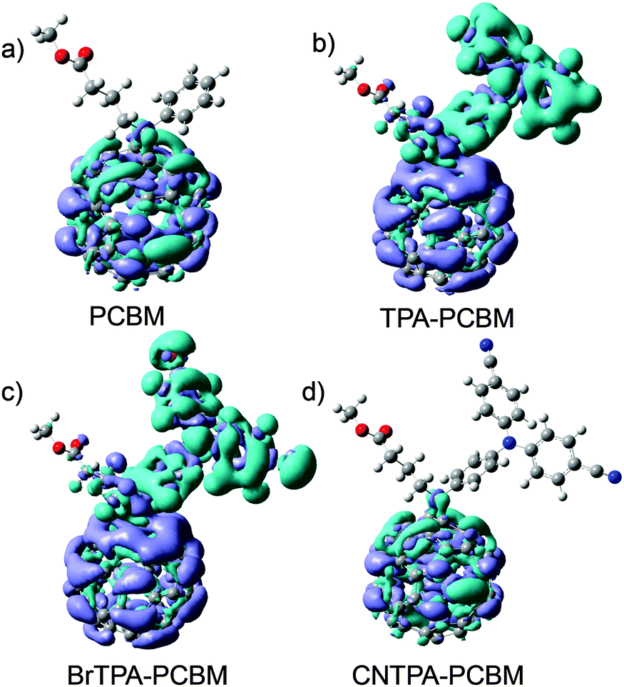 | ||
| Fig. 3 Frontier orbital charge density distribution shown for the lowest excited fullerene (color code: cyan for electrons while light blue represents the hole). | ||
Fig. 4a shows PL spectra of a dilute solution of each fullerene in benzonitrile (dielectric constant, ε = 26.0), and Fig. 4b shows the corresponding PIA spectra. The PL spectral shape remains the same for all fullerenes, and the spectra match previous literature reports for C60 singlet emission.28 We observe quenched emission for CT-fullerenes (TPA–PC61BM and BrTPA–PC61BM) compared to NCT-fullerenes (PC61BM and CNTPA–PC61BM). The PIA spectra of NCT fullerenes both exhibit strong peaks at 780 nm, which has been previously assigned as the triplet absorption band.28,29 In contrast, this triplet absorption band is strongly suppressed in the CT fullerenes. Together, these data suggest that the intramolecular CT state forms faster than the fullerene PL decay (∼1.4 ns), or intersystem crossing times (>1.4 ns for PC61BM).30
 | ||
| Fig. 4 (a) Photoluminescence and (b) photoinduced absorption spectra of diluted fullerene solutions in anaerobic benzonitrile (0.17 mg mL−1). | ||
We further study how the excited CT between fullerenes and TPA affects electron transport of the n-contact layer, finding the enhanced photoexcited charge transport in CT-fullerenes. By evaluating the change in current densities measured in the dark (Jo) and under 1 sun AM 1.5 solar irradiation (Jph) in ITO/ZnO/fullerene/Ca/Al devices, we find that the trend for Jph/Jo enhancement correlates with the increased ratio in dipole moment E(D)/E(G) (Fig. 5 and Table 2).
 | ||
| Fig. 5 Plots of the current density ratio, Jph/Jo, under light and dark conditions along with the calculated dipole change, E(D)/E(G). | ||
CT-fullerenes (TPA–PC61BM and BrTPA–PC61BM) exhibit large enhancement in Jph/Jo (>36 times), while the NCT-fullerenes, PC61BM (6.1 times) and CNTPA–PC61BM (15.3 times), show less prominent change in the Jph/Jo ratio. Although PC61BM itself exhibits relatively better field-effect transistor (FET) and space charge limited current (SCLC) mobilities measured in the dark (Fig. S6–S8, ESI†), the CT-fullerene generates the spatially separated hole on TPA moieties and electrons on the fullerene cage under excitation, a polarized state that results in the optimized inorganic/fullerene interfacial contact and the enhanced fullerene photoconductive effect, especially carrier densities, thus boosting photocurrent and EQE of perovskite PHJ PVs.
Conclusions
In conclusion, we combine new fullerene synthesis, computation, spectroscopy, and device characterization to demonstrate that controlled charge transfer between fullerenes and functional addends allows us to modulate PV performance. Interestingly, these devices do not show the common hysteresis effect observed in many perovskite PVs, which indicates that organic contacts used here can mitigate the perovskite defect states and minimize photocurrent hysteresis in organic/perovskite PHJ solar cells. Fullerenes with intramolecular CT characteristics improve molecular polarization, carrier density, and transport upon excitation, which in turn improve the device operation of PHJ perovskite PVs. It provides a useful model to uncover the fundamental factors to optimize organic–inorganic hybrid electronics.Experimental section
All reactions dealing with air- or moisture-sensitive compounds were carried out using the standard Schlenk technique. P-Tosylhydrazides were synthesized according to literature methods.21,22Synthesis of functional fullerenes
To the dry pyridine (5 mL) solution of methyl-4-(diphenylamino)phenylbenzoylbutyrate tosylhydrazone (0.6 mmol), sodium methoxide (0.6 mmol) was added in one portion under an argon atmosphere. The mixture was stirred at room temperature for 10 min. [60]fullerene (0.42 mmol) in anhydrous ODCB (50 mL) was then transferred to the resulting suspension. The reaction mixture was heated to 75 °C for 40 hours in argon, and then refluxed for additional 5 hours. After cooling to room temperature, the solution was then precipitated with methanol. Chromatography purification on a silica gel column was done to give the product. TPA–PC61BM and BrTPA–PC61BM were purified with the eluent of the toluene–hexane mixture (first 1/4, then toluene/hexane = 1/1). CNTPA–PC61BM was purified with the eluent of toluene, and then with toluene/EA. Spectral data for TPA–PC61BM (36% yield) were identical to the reported one.22 BrTPA–PCBM (40% yield), 1H NMR (CDCl3, δ): 2.22 (m, 2H), 2.56 (t, J = 7 Hz, 2H), 2.90 (m, 2H), 3.70 (s, 3H), 7.04 (d, J = 9 Hz, 4H), 7.16 (d, J = 8.5 Hz, 2H), 7.41 (d, J = 9 Hz, 4H), 7.76 (d, J = 9 Hz, 2H); 13C NMR (CDCl3, δ): 22.96, 34.07, 34.41, 51.80, 52.22, 80.49, 116.84, 106.99, 107.06, 119.28, 123.12, 123.41, 126.74, 131.34, 133.12, 133.53, 138.02, 138.51, 141.27, 141.48, 142.61, 142.62, 142.66, 142.73, 143.44, 143.50, 143.64, 144.27, 144.57, 144.92, 145.01, 145.17, 145.26, 145.30, 145.56, 145.60, 145.65, 145.69, 145.72, 146.32, 146.63, 147.14, 148.27, 149.31, 173.99; ESI HR-mass (C84H21Br2NO2) calcd, 1232.9934; found, 1132.9887. CNTPA–PCBM (30% yield), 1H NMR (CDCl3, δ): 2.23 (m, 2H), 2.58 (t, J = 7.5 Hz, 2H), 2.93 (m, 2H), 3.71 (s, 3H), 7.20 (d, J = 8.5 Hz, 4H), 7.28 (d, J = 9 Hz, 4H), 7.60 (d, J = 9 Hz, 4H), 7.92 (d, J = 9 Hz, 2H); 13C NMR (CDCl3, δ): 22.95, 33.98, 34.31, 51.52, 52.87, 80.12, 106.92, 106.99, 107.06, 119.28, 123.36, 123.41, 124.66, 124.70, 126.96, 127.01, 133.59, 133.66, 134.92, 134.94, 134.97, 135.00, 137.85, 138.59, 141.36, 141.58, 142.54, 142.62, 142.73, 143.51, 143.58, 143.61, 143.70, 144.30, 144.68, 145.00, 145.08, 145.22, 145.25, 145.34, 145.52, 145.65, 145.73, 145.76, 145.80, 146.20, 147.91, 149.02, 150.54, 173.97; ESI HR-mass (C86H21N3O2) calcd, 1127.1628; found, 1127.1639.Perovskite PV fabrication and characterization
The devices were fabricated in the configuration of ITO/PEDOT:PSS/CH3NH3PbI3−xClx/fullerene/fullerene surfactant (C60-bis)/Ag. ITO (15 Ω sq−1) glass substrates were cleaned sequentially with detergent and deionized water, acetone, and isopropanol under sonication for 10 minutes. After drying under a N2 stream, substrates were further cleaned by a plasma treatment for 20 s. PEDOT:PSS (Baytron P VP Al 4083, filtered through a 0.45 μm nylon filter) was first spin-coated onto the substrates at 5k rpm for 30 s and annealed at 150 °C for 10 min in air. Methylammonium iodide (MAI) was synthesized by reacting methylamine (33 wt% in absolute ethanol, Aldrich) and hydroiodic acid (57 wt% in water with 1.5% hypophosphorous acid, Alfa Aesar) at a 2:1 ratio in ethanol at 0 °C for 2 h with stirring in nitrogen. After reaction, MAI precipitation was recovered by rotary evaporation at 40 °C and then dissolved in ethanol. The pure MAI was recrystallized from diethyl ether and dried at 50 °C in a vacuum oven for 24 h. To prepare the perovskite precursor solution, MAI and lead chloride (PbCl2, Aldrich) powders were mixed in anhydrous dimethylformamide (DMF, Aldrich) at a molar ratio of 3:1 with 1 wt% of 1,8-diiodooctane (DIO, Aldrich) with respect to perovskite weight. Perovskite precursors were then deposited through spin-coating at 6k rpm for 45 s (300–500 nm in thickness) and then annealed at 90 °C for 2–3 hours. Afterward, the PCBM/TPA–PCBM/BrTPA–PCBM/CNTPA–PCBM (15 mg mL−1 in chloroform) and C60-bis (2 mg mL−1 in isopropyl alcohol) surfactants were then sequentially deposited by spin coating at 1k rpm for 60 s and 3k rpm for 60 s, respectively. Silver electrodes with a thickness of 150 nm were finally evaporated under high vacuum (<2 × 10⁻⁶ Torr) through a shadow mask. The device area is determined to be 3.14 mm2. All the J–V curves in this study were recorded using a Keithley 2400 source meter unit. The device photocurrent was measured under AM 1.5 illumination conditions at an intensity of 100 mW cm−2. The illumination intensity of the light source was accurately calibrated using a standard Si photodiode detector equipped with a KG-5 filter, which can be traced back to the standard cell of the National Renewable Energy Laboratory (NREL). The EQE spectra recorded here were obtained from an IPCE setup consisting of a Xenon lamp (Oriel, 450 W) as the light source, a monochromator, a chopper with a frequency of 100 Hz, a lock-in amplifier (SR830, Stanford Research Corp), and a Si-based diode (J115711-1-Si detector) for calibration.
Acknowledgements
We acknowledge the DOE SunShot (DE-EE0006710), the AOARD (FA2386–11–1–4072), the ONR (N00014-14-1-0170 and N00014-14-1-246), the NSF (CHE-1265945 & DMR-1215753) and the Boeing Foundation for financial support. D.B.S. is grateful for the NSF Graduate Research Fellowship (No. 2013118402). We thank Dr Yue Zang and Dr Jiang Huang for the SCLC mobility measurements, and Mr Namchul Cho for FET mobility measurements.Notes and references
- A. Kojima, K. Teshima, Y. Shirai and T. Miyasaka, J. Am. Chem. Soc., 2009, 131, 6050 CrossRef CAS PubMed.
- H. Zhou, Q. Chen, G. Li, S. Luo, T.-b. Song, H.-S. Duan, Z. Hong, J. You, Y. Liu and Y. Yang, Science, 2014, 345, 542 CrossRef CAS PubMed.
- H. J. Snaith, J. Phys. Chem. Lett., 2013, 4, 3623 CrossRef CAS.
- N.-G. Park, J. Phys. Chem. Lett., 2013, 4, 2423 CrossRef CAS.
- Q. Wang, Y. Shao, Q. Dong, Z. Xiao, Y. Yuan and J. Huang, Energy Environ. Sci., 2014, 7, 2359 CAS.
- P.-W. Liang, C.-Y. Liao, C.-C. Chueh, F. Zuo, S. T. Williams, X.-K. Xin, J. Lin and A. K. Y. Jen, Adv. Mater., 2014, 26, 3748 CrossRef CAS PubMed.
- J. M. Ball, M. M. Lee, A. Hey and H. J. Snaith, Energy Environ. Sci., 2013, 6, 1739 CAS.
- O. Malinkiewicz, A. Yella, Y. H. Lee, G. M. Espallargas, M. Graetzel, M. K. Nazeeruddin and H. J. Bolink, Nat. Photonics, 2014, 8, 128 CrossRef CAS.
- Q. Lin, A. Armin, R. C. R. Nagiri, P. L. Burn and P. Meredith, Nat. Photonics, 2015, 9, 106 CrossRef CAS.
- Y. Guo, C. Liu, K. Inoue, K. Harano, H. Tanaka and E. Nakamura, J. Mater. Chem. A, 2014, 2, 13827 CAS.
- O. Malinkiewicz, C. Roldán-Carmona, A. Soriano, E. Bandiello, L. Camacho, M. K. Nazeeruddin and H. J. Bolink, Adv. Energy Mater., 2014, 4, 1400345 Search PubMed.
- A. Abrusci, S. D. Stranks, P. Docampo, H.-L. Yip, A. K. Y. Jen and H. J. Snaith, Nano Lett., 2013, 13, 3124 CrossRef CAS PubMed.
- M.-F. Lo, Z.-Q. Guan, T.-W. Ng, C.-Y. Chan and C.-S. Lee, Adv. Funct. Mater., 2015, 25, 1213 CrossRef CAS PubMed.
- K. Wojciechowski, S. D. Stranks, A. Abate, G. Sadoughi, A. Sadhanala, N. Kopidakis, G. Rumbles, C.-Z. Li, R. H. Friend, A. K. Y. Jen and H. J. Snaith, ACS Nano, 2014, 8, 12701 CrossRef CAS PubMed.
- E. J. Juarez-Perez, M. Wußler, F. Fabregat-Santiago, K. Lakus-Wollny, E. Mankel, T. Mayer, W. Jaegermann and I. Mora-Sero, J. Phys. Chem. Lett., 2014, 5, 680 CrossRef CAS.
- C.-Z. Li, C.-C. Chueh, H.-L. Yip, J. Zou, W.-C. Chen and A. K. Y. Jen, J. Mater. Chem., 2012, 22, 14976 RSC.
- T. Leijtens, S. D. Stranks, G. E. Eperon, R. Lindblad, E. M. J. Johansson, I. J. McPherson, H. Rensmo, J. M. Ball, M. M. Lee and H. J. Snaith, ACS Nano, 2014, 8, 7147 CrossRef CAS PubMed.
- G. Xing, N. Mathews, S. Sun, S. S. Lim, Y. M. Lam, M. Grätzel, S. Mhaisalkar and T. C. Sum, Science, 2013, 342, 344 CrossRef CAS PubMed.
- S. D. Stranks, G. E. Eperon, G. Grancini, C. Menelaou, M. J. P. Alcocer, T. Leijtens, L. M. Herz, A. Petrozza and H. J. Snaith, Science, 2013, 342, 341 CrossRef CAS PubMed.
- P. Gao, M. Gratzel and M. K. Nazeeruddin, Energy Environ. Sci., 2014, 7, 2448 CAS.
- C.-Z. Li, S.-C. Chien, H.-L. Yip, C.-C. Chueh, F.-C. Chen, Y. Matsuo, E. Nakamura and A. K. Y. Jen, Chem. Commun., 2011, 47, 10082 RSC.
- Y. Zhang, H.-L. Yip, O. Acton, S. K. Hau, F. Huang and A. K. Y. Jen, Chem. Mater., 2009, 21, 2598 CrossRef CAS.
- K. M. O'Malley, C.-Z. Li, H.-L. Yip and A. K. Y. Jen, Adv. Energy Mater., 2012, 2, 82 CrossRef PubMed.
- C.-Z. Li, C.-Y. Chang, Y. Zang, H. X. Ju, C.-C. Chueh, P. W. Liang, N. Cho, D. S. Ginger and A. Y. K. Jen, Adv. Mater., 2014, 26, 6262 CrossRef CAS PubMed.
- C.-Z. Li, C.-C. Chueh, H.-L. Yip, F. Ding, X. Li and A. K. Y. Jen, Adv. Mater., 2013, 25, 2457 CrossRef CAS PubMed.
- W. Nie, H. Tsai, R. Asadpour, J.-C. Blancon, A. J. Neukirch, G. Gupta, J. J. Crochet, M. Chhowalla, S. Tretiak, M. A. Alam, H.-L. Wang and A. D. Mohite, Science, 2015, 347, 522 CrossRef CAS PubMed.
- Y. Shao, Z. Xiao, C. Bi, Y. Yuan and J. Huang, Nat. Commun., 2014, 5, 5784 CrossRef CAS PubMed.
- C. W. Schlenker, K.-S. Chen, H.-L. Yip, C.-Z. Li, L. R. Bradshaw, S. T. Ochsenbein, F. Ding, X. S. Li, D. R. Gamelin, A. K. Y. Jen and D. S. Ginger, J. Am. Chem. Soc., 2012, 134, 19661 CrossRef CAS PubMed.
- A. Rao, P. C. Y. Chow, S. Gelinas, C. W. Schlenker, C.-Z. Li, H.-L. Yip, A. K. Y. Jen, D. S. Ginger and R. H. Friend, Nature, 2013, 500, 435 CrossRef CAS PubMed.
- P. C. Y. Chow, S. Albert-Seifried, S. Gélinas and R. H. Friend, Adv. Mater., 2014, 26, 4851 CrossRef CAS PubMed.
Footnote |
| † Electronic supplementary information (ESI) available: Experimental details, and supplementary scheme and figures referred in the text. See DOI: 10.1039/c5mh00026b |
| This journal is © The Royal Society of Chemistry 2015 |