Highly aligned polymer nanowire-based fin architecture for enhanced functionality of organic electrochemical transistors in neuromorphic computing
Received
16th September 2025
, Accepted 12th November 2025
First published on 17th November 2025
Abstract
Despite rapid advances in organic neuromorphic electronics, achieving linear and stable synaptic plasticity in organic electrochemical transistors (OECTs) remains challenging. Here, we show that imposing high alignment and nanoscale confinement in poly[2,5-bis(3-tetradecylthiophen-2-yl)thieno[3,2-b]thiophene] (PBTTT-C14) conjugated polymer nanowires (NWs)—organized as a fin architecture—directly enhances ion–polymer interactions and regulates ion transport, thereby improving OECT functionality relevant to neuromorphic computing. Uniform, highly aligned NWs are formed by solution nanomolding using a polydimethylsiloxane (PDMS) mold. The resulting fin-structured OECTs (FinOECTs) exhibit a μC* value, where μC* is the product of the volumetric capacitance (C*) and charge carrier mobility (μ), of 10.24 F V−1 s−1 cm−1, approximately twofold higher than those of film-based control devices. Structural analysis confirms increased crystallinity (coherence length 508.9 Å) and tighter π–π stacking, consistent with confinement-driven ordering that supports efficient mixed conduction. Most importantly, the alignment-driven fin geometry yields highly linear synaptic responses in both long-term potentiation (LTP) and long-term depression (LTD) (R2 of 0.997), by moderating otherwise rapid ion diffusion at the NW–ion–gel interface. The devices also exhibit robust long-term memory (LTM), retaining 46.16% of the excitatory postsynaptic current after 1000 s. Finally, FinOECT-based reservoir computing attains a structural similarity index of 0.80 on a 16 × 16 pattern recognition task. These results establish highly-aligned polymeric NW fin architectures as a materials- and structure-level route for linear, durable and energy-efficient OECT-based neuromorphic computing systems.
1. Introduction
The field of organic electronics has advanced rapidly in recent years, offering distinct advantages over silicon-based technologies, including mechanical flexibility,1–5 cost-effective solution processability,6–9 and inherent biocompatibility,10–13 which together enable applications from wearable devices to biomedical systems. In addition, the structural tunability of organic materials allows precise control of electronic properties and device functionality through molecular design.14–18 In parallel, neuromorphic computing has emerged as a promising route to overcome the limitations of von Neumann architectures, particularly for artificial intelligence (AI), by emulating the architecture and function of biological neural networks and thereby enabling more energy-efficient and scalable computing.19–23
Among candidate device platforms, organic electrochemical transistors (OECTs) are strong contenders for artificial synapses. Their low-voltage operation (typically <1 V), excellent biocompatibility, and intrinsic ionic–electronic coupling closely resemble biological synaptic behavior.24–28 In OECTs, channel conductivity is modulated by the interaction between electrolyte ions and charge carriers in organic semiconductors (OSCs) under an applied gate voltage (VGS), an ion–electron coupling mechanism analogous to synaptic weight updates driven by ion flux in biology. While biological synapses typically exhibit gradual, near-linear weight changes, achieving similarly linear synaptic plasticity in artificial devices remains challenging. Many OECT-based synaptic devices still show non-linear weight updates, which limits computational efficiency.29–31 A principal reason is the rapid back-diffusion of ions into the electrolyte after removal of the gate stimulus, an effect exacerbated in conventional planar OECTs, where large, unconfined channels facilitate fast ion redistribution. These constraints motivate alternative device architectures that regulate ion dynamics to realize linear and stable synaptic behavior.
To address this, we adopt a fin field-effect transistor (FinFET)-inspired strategy: translating the three-dimensional fin architecture of silicon technology into the mixed ionic–electronic conduction context of OECTs. FinFETs leverage vertically oriented fins to enhance electrostatic control through an increased surface-to-volume ratio and geometric confinement.32,33 Analogously, we engineer highly aligned conjugated polymer nanowires (NWs) arranged as fins to deliberately amplify the polymer–ion interfacial area and impose nanoscale confinement on ion-transport. This architecture is designed to (i) increase accessible ion–polymer interaction sites along fin sidewalls and (ii) suppress rapid ion back-diffusion, thereby promoting uniform electrochemical doping and more linear, stable synaptic weight updates. The emphasis on high alignment ensures well-defined pathways and reproducible interfacial geometry, linking nanoscale structures to controllable ion dynamics and neuromorphic functionality.
Prior work supports the efficacy of lateral access and geometric structuring for enhancing OECT performance. For example, C. Yan et al. showed that micropatterned OECTs with laterally intercalated ion pathways, produced by photolithography, exhibited substantially enhanced volumetric ion charging; the striped OSC patterns delivered >600% improvement in maximum transconductance relative to response time, attributed to ion penetration through lateral faces of the semiconductor.34 Beyond performance gains, those studies provided mechanistic insight into how lateral structuring improves doping uniformity, an essential ingredient for linear synaptic updates. Building on this foundation, our FinFET-inspired polymeric nanowire fin architecture explicitly targets maximization of polymer–ion interactions and ion-transport confinement, providing a materials- and structure-level route to linear, durable, and energy-efficient OECT neuromorphic systems.
Here, we implement this FinFET-inspired design by developing FinOECTs that incorporate highly aligned thiophene-based conjugated polymer nanowire (NW) fins. For material selection, poly(3-hexylthiophene) (P3HT) was chosen as a benchmark reference polymer due to its well-established electronic behavior, while poly[2,5-bis(3-tetradecylthiophen-2-yl)thieno[3,2-b]thiophene] (PBTTT)—its higher-crystallinity analogue with extended conjugation and longer side chains—was selected to elucidate the influence of molecular ordering and backbone rigidity on FinOECT performance. Uniform, high-aspect-ratio NW fins are produced via a solution nanomolding/stamping process with optimized conditions to ensure reproducible pitch, width, and alignment. Their morphology is verified by optical microscopy (OM), scanning electron microscopy (SEM), and atomic force microscopy (AFM), while ultraviolet-visible (UV-Vis) spectroscopy and X-ray diffraction (XRD) confirm enhanced crystallinity and tighter π–π stacking relative to control films. Charge-transport properties are benchmarked using companion organic field-effect transistors (OFETs), and mixed ionic–electronic conduction is quantified in OECTs. Compared with conventional planar, film-based OECTs, the fin architecture increases the accessible polymer–ion interfacial area and imposes nanoscale confinement on ion-transport, leading to higher μC*, improved transconductance at sub-1 V operation, and markedly more linear synaptic weight updates (R2 near unity) by suppressing rapid ion back-diffusion and promoting uniform electrochemical doping at NW–electrolyte interfaces. Finally, we validate system-level relevance using a reservoir-computing image-recognition task, demonstrating that device-level linearity and retention translate into practical neuromorphic functionality with low operating voltage. Collectively, this work (i) establishes a scalable, solution-processable route to aligned polymer nanowire fin architectures, (ii) elucidates a direct structure–transport–function link between alignment/confinement and synaptic linearity in OECTs, and (iii) positions FinOECTs as a viable material- and architecture-level platform for energy-efficient, bio-inspired computing.
2. Experimental section
2.1. Materials
PBTTT and P3HT (>99% purity) were purchased from Sigma-Aldrich. 1,2,3,4-Tetrahydronaphthalene (Tetralin, 99%) was obtained from Sigma Aldrich. SiO2 (300 nm)/Si wafer and Au pellets (3 mm diameter × 3 mm thickness, 99.99% purity) were supplied by iTASCO. 1-Ethyl-3-methylimidazolium bis(trifluoromethylsulfonyl)imide (EMIM:TFSI, ≥98%) and poly(vinylidene fluoride-co-hexafluoropropylene) (PVDF-HFP, Mw ≈ 400![[thin space (1/6-em)]](https://www.rsc.org/images/entities/char_2009.gif) 000) were purchased from Sigma-Aldrich. Toluene (99.5%, C6H5CH3), 2-propanol (IPA, 99.5%, (CH3)2CHOH), and acetone (99.7%, CH3COCH3) were purchased from Samchun Chemicals (South Korea).
000) were purchased from Sigma-Aldrich. Toluene (99.5%, C6H5CH3), 2-propanol (IPA, 99.5%, (CH3)2CHOH), and acetone (99.7%, CH3COCH3) were purchased from Samchun Chemicals (South Korea).
2.2. Substrate preparation
SiO2 (300 nm)/Si wafer was sequentially cleaned by ultrasonication in acetone and IPA for 10 min each, followed by drying with nitrogen gas. Subsequently, to remove organic residues, substrates were treated with ultraviolet ozone (UV ozone cleaner) for 300 s. For hydrophobic surface treatment, substrates were immersed in a solution composed of 100 mL hexane and 0.3 mL octadecyltrichlorosilane (OTS) for 30 min. After immersion, substrates were rinsed with ethanol to remove residual OTS and annealed on a hot plate at 120 °C for 20 min. Following annealing, substrates were immersed in chloroform and ultrasonicated for 5 min and then dried under nitrogen gas.
2.3. Stamping-mold fabrication
PDMS molds were fabricated using a Sylgard 184 kit (Dow Corning). Polyurethane acrylate (PUA) was purchased from MINS-ERM, Minuta Tech. PDMS precursor and curing agent were mixed at a 10:1 ratio, degassed in a vacuum desiccator for 10 min to remove bubbles, poured into a Petri dish, and cured at 80 °C in an oven for 1 h to produce the PDMS support layer. The cured PDMS support was subsequently cut into appropriate sizes for further use. A silicon master mold was fabricated by electron-beam (E-beam) lithography (Fig. S1(a)). To facilitate separation, the silicon master mold was surface-treated with 1H,1H,2H,2H-perfluorooctyltriethoxysilane (FTS). FTS was diluted in hexane (0.55 mL:50 mL) and deposited onto the silicon mold surface as a self-assembled monolayer through vapor deposition under mild vacuum conditions in a desiccator for 60 min. A small amount of PUA was then dropped onto the PDMS support, and the FTS-treated silicon master mold was placed on top (Fig. S1(b)). The composite mold was UV-cured for 15 min, after which the silicon master mold was carefully detached to yield the final PUA/PDMS mold (Fig. S1(c) and (d)).
2.4. Fabrication of polymer NWs
PBTTT and P3HT were dissolved in Tetralin at a concentration of 10 mg mL−1. Polymer nanowires (NWs) were fabricated using the liquid-bridge-mediated nano-transfer molding (LB-nTM) technique.35,36 Initially, the prepared OSC solution was deposited onto an OTS-treated wafer (Fig. 1(a)). The PUA/PDMS mold was then aligned (Fig. 1(b)) and gently pressed to form a liquid bridge (Fig. 1(c)). The sample was dried on a hot plate at 160 °C for 4 h and further annealed in a vacuum chamber at 120 °C for 2 h. Finally, the mold was removed to produce the NW patterns (Fig. 1(d)).
 |
| | Fig. 1 Schematic illustration of the liquid-bridge-mediated nanotransfer molding (LB-nTM) process used to fabricate aligned polymer nanowire arrays. (a) After hydrophobic surface modification of SiO2 (300 nm)/Si substrates, diluted semiconducting polymer solutions of P3HT and PBTTT were dispensed onto the treated substrates. (b) A PDMS mold with a thin polyurethane-acrylate (PUA) layer was gently laminated onto the polymer solution. The advancing meniscus selectively filled only the recessed grooves via discontinuous dewetting, leaving the ridges uncoated. (c) The filled mold was then placed in contact with the OTS-treated substrate through a thin polar liquid layer that formed a capillary bridge, generating Laplace-driven forces that ensured intimate contact and complete pattern transfer. (d) After evaporation and gentle demolding, continuous and directionally aligned polymer nanowires were obtained, replicating the mold geometry. Device structures (left) and synaptic potentiation/depression properties (right) of (e) OSC film-based and (f) OSC NW-based FinOECTs. | |
2.5. Fabrication of OFETs and FinOECTs
Au electrodes (60 nm thickness) were thermally evaporated onto the OSC NWs through a shadow mask under vacuum conditions (10−6 Torr) to define a channel with a width (W) of 1000 µm and a length (L) of 50 µm. An ionic liquid gel electrolyte was prepared by dissolving 0.5 g of PVDF-HFP and 2 g of EMIM:TFSI in 10 mL of acetone and stirring the mixture at 50 °C for 2 h. To fabricate OECTs, the prepared EMIM:TFSI ion gel electrolyte was deposited onto the polymer NW sample.
2.6. Characterization techniques
The electrical characteristics of the OFET and OECT were evaluated using a semiconductor probe station equipped with a Keithley 2636B source-measure unit. The surface morphologies of polymer films and NWs were characterized by optical microscopy (OM; Olympus BX53M), atomic force microscopy (AFM; Tosca™ 400, Anton Paar), and field emission scanning electron microscopy (SEM; TESCAN MIRA LMS). The crystallinity of the polymer NWs was analyzed using X-ray diffraction (XRD; Rigaku Ultima IV diffractometer). The absorption spectra of OSC films were recorded using ultraviolet-visible-near infrared (UV-vis-NIR) spectroscopy (JASCO V-670 spectrophotometer).
3. Results and discussion
3.1. Fabrication and physical characterization of polymer NWs
Fig. 1(a)–(d) schematically illustrates the fabrication sequence of highly-aligned polymer nanowires prepared via a liquid-bridge-mediated nanotransfer molding method (LB-nTM). Prior to patterning, SiO2 (300 nm)/Si substrates were hydrophobically modified with OTS to promote edge-on crystal orientation of the polymer semiconductors. Dilute solutions of P3HT or PBTTT were then dispensed onto the treated substrates (Fig. 1(a)). The PDMS mold with a thin nano-patterned PUA layer to suppress solvent-induced swelling and enhance mechanical rigidity was subsequently aligned and brought into gentle contact with the polymer ink (Fig. 1(b)). Selective inking occurred through discontinuous dewetting, whereby the advancing meniscus of the polymer solution filled only the recessed nanoscale grooves of the mold while leaving the raised ridges uncoated. This self-limiting process, governed by the low surface free energy of PUA (∼20 mJ m−2) and the interfacial energy balance between the mold and the solution, ensures precise confinement of the ink within the patterned trenches.35,36 Upon mild drying, the solvent gradually evaporated, leading to the self-assembly and crystallization of polymer chains within the confined channels, forming solidified nanowire precursors (Fig. 1(c)). For nanowire transfer, the filled mold was placed onto the OTS-treated substrate pre-wetted with a thin polar liquid layer, which established a capillary bridge between the mold and the substrate. During solvent evaporation, Laplace-driven capillary forces drew the nanowires into intimate conformal contact with the substrate surface without the need for external pressure.35,36 As the liquid bridge evaporated completely, the mold was gently peeled away, leaving behind highly aligned, continuous polymer nanowires faithfully replicated from the mold geometry (Fig. 1(d)). This integrated sequence—comprising selective inking, confined self-assembly, and capillary-mediated transfer—enables reproducible formation of directionally aligned polymer nanowire arrays with enhanced crystalline order and strong substrate adhesion.
Typically, OECTs employing p-type OSC film structures exhibit good linearity in potentiation mode, wherein anions from the ion gel electrolyte penetrate and dope the OSC, thereby increasing channel conductivity under negative VGS (Fig. 1(e)).37 Conversely, these film-based OECTs commonly show poor linearity in depression mode due to rapid ion back-diffusion into the electrolyte upon application of positive VGS. In contrast, polymer NW-based structures have the potential to achieve linear depression characteristics, attributed primarily to slower ion diffusion resulting from the confined NW geometry, in addition to linear potentiation facilitated by electric drift (Fig. 1(f)). S. Wang et al. previously reported that OECTs featuring an ion gel fully encapsulating the OSC channel exhibited uniform electric fields, thereby enabling consistent and controlled ion diffusion throughout the entire OSC structure.38 In the current study, we implemented FinOECTs by coating ion gels on top of the patterned OSC NW channels.
The PDMS molds were replicated from silicon master molds patterned by electron-beam lithography, enabling precise transfer of nanoscale line features. The resulting polymer nanowires (NWs) of PBTTT and P3HT accurately reproduced the master mold geometry, as confirmed by optical microscopy (OM) images in Fig. 2(a)–(c). Both the Si and PUA/PDMS composite molds exhibited highly uniform periodic patterns, verifying excellent replication fidelity. Extended-view OM and SEM images of the patterned films revealed continuous, well-aligned NW arrays with high pattern regularity for both PBTTT (Fig. 2(d)) and P3HT (Fig. 2(e)). AFM height and phase analyses (Fig. S2 and S3) further confirmed the successful formation of well-defined OSC NWs on OTS-treated SiO2/Si substrates. These results collectively confirm that the LB-nTM process ensures accurate pattern transfer and reproducible nanowire morphology.
 |
| | Fig. 2 Morphological and structural characterization of polymer nanowires (NWs) fabricated by liquid-bridge-mediated nanotransfer molding (LB-nTM). Optical microscopy (OM) images of the (a) Si master mold, (b) replicated PUA/PDMS composite mold, and (c) patterned PBTTT and P3HT NW arrays. Insets show the corresponding SEM images of the Si and PUA/PDMS molds, confirming high-fidelity pattern replication. (d) and (e) SEM images of aligned PBTTT and P3HT NWs, respectively. (f) UV-Vis absorption spectra of PBTTT (upper) and P3HT (lower) in quenched films, annealed films, and nanowires. (g) and (h) XRD patterns of PBTTT and P3HT in thin-film (left) and NW (right) configurations, demonstrating well-defined (h00) and (010) reflections indicative of high crystallinity and ordered molecular packing. | |
Fig. 2(f) presents UV-Vis absorption spectra of PBTTT (upper) and P3HT (lower) films immediately after spin-coating (“quenched”), after annealing (“annealed”), and in the form of polymer NWs. Quenched films typically contain amorphous regions, structural defects, and grain boundaries, resulting in reduced intra-chain order and thus exhibiting blue-shifted absorption spectra at higher photon energies, consistent with previous studies.39 On the other hand, increased crystallinity in annealed films and NWs reduces grain boundaries, structural defects, and amorphous domains, thereby extending conjugation lengths and creating highly planarized, fully delocalized electronic states along polymer backbones. These structural enhancements result in red-shifted absorption spectra, signifying significantly improved crystallinity. Furthermore, additional distinct peaks at wavelengths of 600 and 660 nm were observed in the UV-Vis spectra of polymer NWs. These features indicate enhanced crystallinity due to H-aggregate formation, originating from interchain (Frenkel) exciton delocalization facilitated by effective π–π stacking between polymer chains.40Fig. 2(g) and (h) show a comparison of the XRD spectra of PBTTT and P3HT films and their corresponding NW structures. Detailed crystallinity parameters extracted from these spectra are summarized in Table 1. Compared to the PBTTT film with a coherence length of 157.0 Å and a π–π stacking distance of 3.91 Å, the PBTTT NWs had a 3.2 times improved coherence length of 508.9 Å and a π–π stacking distance of 3.87 Å, shortened due to H-aggregation by confinement of OSC molecules induced by PDMS stamping. Additionally, PBTTT NWs showed additional XRD peaks such as those at (300) and (400), indicating enhanced crystallinity in various directions. P3HT NWs also exhibited a coherence length of 460.2 Å, which was twice higher than that of the P3HT film (211.4 Å), and a π–π stacking distance of 3.87 Å, which was shorter than that of the P3HT film (3.90 Å).
Table 1 Crystallographic characteristics of PBTTT and P3HT NWs and films showing lamellar stacking distance, crystal size and π–π stacking distance
|
|
(100) peak |
(010) peak |
|
|
q (Å−1) |
d-spacing (Å) |
FWHM (Å−1) |
Coherence length (Å) |
q (Å−1) |
π–π stacking (Å) |
| PBTTT NW |
0.415 |
15.15 |
0.0111 |
508.9 |
1.622 |
3.87 |
| P3HT NW |
0.508 |
12.37 |
0.0123 |
460.2 |
1.624 |
3.87 |
| PBTTT film |
0.534 |
11.76 |
0.0361 |
157.0 |
1.606 |
3.91 |
| P3HT film |
0.811 |
7.74 |
0.0268 |
211.4 |
1.609 |
3.90 |
3.2. Electrical performance of polymer NW OFETs
To analyze the electrical characteristics of polymer OSC NWs, OFETs based on PBTTT and P3HT NWs with bottom gate and top contact structures were fabricated and their characteristics were compared with those of OFETs based on polymer OSC films. Fig. 3(a)–(d) and Table 2 show the transfer curves at a drain voltage (VDS) of −40 V of PBTTT and P3HT NWs compared with the corresponding films. Five devices were measured for statistical analysis in this study. PBTTT and P3HT NWs exhibited high mobility (μ) values of 1.47 × 10⁻¹ and 9.03 × 10⁻³ cm2 V−1 s−1, compared to 4.61 × 10⁻² and 8.96 × 10⁻³ cm2 V−1 s−1 for the corresponding film, respectively, calculated from the following equation in saturation regime:| |  | (1) |
where IDS is the drain current, Cox is the capacitance per unit area of the total gate dielectric layer (Cox = 1.15 × 10⁻⁸ F cm−2 for 300 nm SiO2) and Vth is the threshold voltage. The W of OSC NWs was measured from the OM images in the inset of Fig. 3(a) and (b). The high electrical performance of NWs appears to be due to the confined crystal formation effect during the nanopatterning process using a mold. Noteworthily, PBTTT and P3HT NWs exhibited reduced Ion/Ioff (where Ion is the on-current and Ioff is the off-current) of 3.93 × 10² and 4.64 × 10⁴ compared to 1.30 × 10⁶ and 1.93 × 10⁶ for the film due to the p-type doping effect by the long organic solvent retention time during the solution-based nanopatterning process. In addition, Fig. S4 shows the transfer curves of OFETs based on OSC NWs compared to films at a VDS of −10 V, and the NWs showed enhanced μ and reduced Ion/Ioff as above, calculated from the following equation in the linear regime:| | 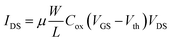 | (2) |
 |
| | Fig. 3 Electrical characteristics of polymer NW OFETs compared to polymer films. Transfer curves of (a) PBTTT NWs, (b) P3HT NWs, (c) PBTTT film and (d) P3HT film at a VDS of −40 V (inset: OM images and device structures of OFETs; scale bar: 0.5 mm). Output curves of (e) PBTTT NWs, (f) P3HT NWs, (g) PBTTT film and (h) P3HT film. | |
Table 2 Electrical performance of PBTTT and P3HT OFETs according to their film and NW structures. 5 devices were statistically analyzed
| OSC |
W/La |
V
DS
(V) |
μ
(cm2 V−1 s−1) |
V
th
(V) |
I
on/Ioffe |
|
Channel width/channel length.
Drain voltage.
Charge carrier mobility of OFETs.
Threshold voltage.
On current and off current ratio.
Standard deviation of properties.
|
| PBTTT film |
20 |
−10 |
1.85 (±0.84)f × 10−2 |
1.78 (±0.83) |
4.30 (±0.59) × 105 |
| −40 |
4.61 (±0.87) × 10−2 |
−4.44 (±0.99) |
1.30 (±0.63) × 106 |
| P3HT film |
20 |
−10 |
4.94 (±0.51) × 10−3 |
−15.07 (±1.25) |
8.81 (±0.39) × 105 |
| −40 |
8.96 (±0.36) × 10−3 |
−18.05 (±2.53) |
1.93 (±0.86) × 106 |
| PBTTT NW |
7.55 |
−10 |
3.98 (±0.29) × 10−2 |
−2.50 (±0.21) |
6.00 (±0.17) × 103 |
| −40 |
1.47 (±0.13) × 10−1 |
−12.57 (±0.50) |
3.93 (±0.85) × 102 |
| P3HT NW |
5.71 |
−10 |
1.19 (±0.13) × 10−2 |
−0.72 (±0.45) |
1.72 (± 0.21) × 104 |
| −40 |
9.03 (±0.39) × 10−3 |
−1.05 (±0.25) |
4.64 (± 0.72) × 104 |
Fig. 3(e)–(h) show the output curves of OFETs based on NWs of PBTTT and P3HT compared to films, showing similar trends with transfer curves, IDS saturation behavior and negligible hysteresis, indicating low trap sites. Even though the low IDS of the NWs is due to small W, the polymer OSC NW-based OFETs exhibited high electrical properties induced by the enhanced charge transfer characteristics in the direction of the polymer OSC NWs, induced by the confinement of the OSC crystal shown in Fig. 2(f)–(h).
3.3. Electrical characteristics of FinOECTs
Fig. 4(a) and (b) present transfer characteristics of FinOECTs employing PBTTT and P3HT NWs at a VDS of −0.5 V; the corresponding electrical figures of merit are summarized in Table 3. The mixed ionic–electronic transport is quantified using μC*, where C* is the volumetric capacitance of the ion gel and μ is the charge carrier mobility in the OSC channel. We extract μC* from the transconductance relation:| | 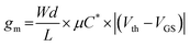 | (3) |
with the NW channel thickness d = 50.51 nm. PBTTT- and P3HT-based FinOECTs yield μC* values of 10.24 and 5.03 F V−1 s−1 cm−1, respectively, exceeding those of their film counterparts (4.49 and 3.29 F V−1 s−1 cm−1 in Fig. S5(a) and (b)), consistent with enhanced crystalline order and more efficient charge transport observed in companion OFETs. Because the PDMS mold used for NW fabrication bears finite surface roughness, this texture can be imprinted onto the NW sidewalls, increasing interfacial tortuosity and partially impeding ion ingress from the ion gel. This manifests as a more negative Vth for NW devices relative to films (PBTTT: −1.31 V vs. −0.28 V; P3HT: −1.45 V vs. −1.41 V), indicating that a larger |VGS| is required to initiate comparable ionic doping in the confined NW channels. Output characteristics (Fig. 4(c), (d) and Fig. S5c and d) show the expected increase of IDS with VDS in both PBTTT and P3HT FinOECTs. Notably, PBTTT NW devices exhibited pronounced hysteresis (Fig. S6), attributable to slower ion penetration/release dynamics at their more hydrophobic interfaces (water contact angle 90°, Fig. S7(a)) compared to P3HT (76°, Fig. S7(b)). This interfacial ion-exchange asymmetry, together with superior structural order, highlights the suitability of PBTTT-based FinOECTs for neuromorphic operation. The polymer-specific origins of this performance gap are consistent with known structure–property relationships. PBTTT readily forms highly crystalline domains in confined geometries owing to its rigid fused thienothiophene backbone and long tetradecyl (C14) side chains. The fused core restricts rotational freedom, promotes backbone planarization, and enhances π–π orbital overlap, while the long alkyl chains facilitate interdigitation across lamellae, enabling tighter packing and fewer structural defects.41–43 By contrast, P3HT's single-thiophene repeat unit affords greater torsional freedom, leading to non-planar conformations, increased π–π spacing, and larger amorphous fractions; densely packed hexyl (C6) side chains further introduce steric hindrance that limits efficient lamellar packing.44–48 In our stamping process, only partial confinement (without external pressure) was applied; accordingly, large-scale molecular rearrangements were not fully realized. Nevertheless, XRD, as shown in Fig. 2(g) and (h), evidences confinement-induced crystallinity gains in PBTTT, which help preserve the structural order against ion penetration and thereby sustain excellent FinOECT performance. In contrast, P3HT NWs are more susceptible to crystallinity degradation upon ionic doping, yielding comparatively lower electrical metrics.
 |
| | Fig. 4 Electrical properties of FinOECTs based on polymer NWs. Transfer characteristics of FinOECTs based on (a) PBTTT NWs and (b) P3HT NWs at a VDS of −0.5 V. Output characteristics of FinOECTs based on (c) PBTTT NWs and (d) P3HT NWs. Comparison of the operation mechanism in (e) electrostatic (interfacial) gating and (f) electrochemical (volumetric) gating. | |
Table 3 Electrical performance of PBTTT and P3HT OECTs according to their film and NW structures (VDS = −0.5 V). 5 devices were statistically analyzed
| OSC |
W/L
|
μC*b (F V−1 s−1 cm−1) |
V
th
(V) |
I
on/Ioffd |
|
Channel width/channel length.
Charge carrier mobility of OECTs.
Threshold voltage.
On current and off current ratio.
Standard deviation of properties.
|
| PBTTT film |
20 |
4.49 (±0.48)e |
−0.28 (±0.05) |
8.48 (±7.20) × 103 |
| P3HT film |
20 |
3.29 (±0.45) |
−1.41 (±0.02) |
2.25 (±2.21) × 103 |
| PBTTT NW |
10 |
10.24 (±0.27) |
−1.31 (±0.14) |
4.39 (±1.47) × 103 |
| P3HT NW |
7 |
5.03 (±0.51) |
−1.45 (±0.10) |
5.72 (±1.55) × 104 |
These observations can be rationalized within the unified electrolyte-gated transistor (EGT) framework,49 which casts gate coupling as an effective capacitance Ceff arising from interfacial double-layer capacitances in series with the semiconductor's chemical (DOS-dependent) capacitance. As gate bias modulates carrier density and tail-state filling (disorder parameter σ), Ceff evolves continuously between two limits. In electrostatic (interfacial) gating (Fig. 4(e)), the chemical capacitance is negligible (typical of ordered channels and/or higher doping), giving Ceff → CDL. In electrochemical (volumetric) gating (Fig. 4(f)), the chemical capacitance dominates (typical of disordered, less confined channels), producing thickness-dependent responses in which the conventional “volumetric capacitance” C* emerges from DOS parameters. In the small-bias/disordered limit, the model recovers IDS ∝ μC*d(VGS − VT); in the high-doping/ordered limit, the slope approaches μCDL. Within this framework, our PBTTT NW fins – combining higher crystallinity, tighter π–π stacking, and laterally accessed, hydrophobic interfaces – suppress deep electrolyte percolation and favor sidewall-localized, interfacial gating, consistent with the more negative Vth, pronounced hysteresis, and high μ inferred from OFETs. Thus, despite the large extracted μC*, the capacitive leverage in the neuromorphic operating window (LTP/LTD) is predominantly interfacial, placing NW FinOECTs nearer the electrostatic EGT limit. Conversely, the planar films present larger, less confined volumes and greater energetic/morphological disorder, as shown in Fig. 1(e), for which the EGT model predicts dominant chemical capacitance at modest bias and explicit thickness scaling, i.e., the electrochemical (volumetric) OECT regime where IDS ≈ μC*d. The film devices’ less negative Vth and their transfer-curve shapes are fully consistent with this assignment. Together, the structural, interfacial, and EGT-based analyses provide a coherent rationale for the distinct gating regimes of NW-fin versus film OECTs and clarify how alignment and confinement translate into the improved linearity and stability required for neuromorphic computing.
3.4. Neuromorphic properties of FinOECTs
In a biological synapse, an input pulse of electrical stimulation from one neuron transmits a signal as an excitatory postsynaptic potential (EPSC) to the next neuron. In this way, OSC NWs can be doped by ion permeation from the surrounding ion gel induced by pulse-type electrical stimulation of VGS in FinOECTs to transmit signals as EPSCs to IDS (Fig. 5(a)). In pulse count mode, with 10 pulses of −1.5 V, PBTTT NWs (Fig. 5(b)) exhibited short-term plasticity (STP) characteristics, and the higher EPSC of 49.81% was maintained as the baseline after 5 s from the end of the pulses compared to the PBTTT film (28.49%) (Fig. S8(a)). In voltage sweep mode with pulses from −0.2 to −2 V (increased by −0.2 V step), PBTTT NWs (Fig. 5(c)) showed gradually increased EPSCs, and the higher EPSC of 55.73% was maintained as a baseline after 5 s from the end of the pulses compared to the PBTTT film (49.60%) (Fig. S8(b)). In the width sweep mode where the pulse width of −1.5 V pulse was adjusted from 0.1 to 1 s (increased by 0.1 s steps) and the interval was adjusted from 0.9 to 0.1 s (decreased by 0.1 s steps), PBTTT NWs (Fig. 5(d)) showed that the EPSCs gradually increased with increasing pulse width, and the similar EPSC of 30.00% to that of the PBTTT film (Fig. S8(c)) was maintained as a baseline at 5 s after the end of the pulses because of the shortening interval between pulses. Fig. 5(e) and Fig. S8(d) show a gradually increased paired pulse, which is the ratio of EPSCs at two consecutive peaks as the pulse interval decreases for PBTTT NWs and PBTTT films, calculated from the following:| |  | (4) |
where A1 and A2 are the first and second EPSCs from peaks. At 0.1 s of the interval, the paired pulse facilitation of PBTTT NWs was calculated as a higher value of 206.57% compared to that of PBTTT films (152.17%), showing STP properties as biological synapses. To quantitatively compare the response speed, the paired pulse facilitation behavior was fitted using a two-phase exponential decay function:| | | Paired pulse facilitation = C0 + C1e−Δt/t1 + C2e−Δt/t2 | (5) |
where C1 and C2 are the amplitudes, t is the time, and t1 and t2 represent fast and slow ionic relaxation time constants, respectively. These time constants reflect distinct kinetic components of ionic redistribution where t1 corresponds to the rapid redistribution of ions near the channel–electrolyte interface and within readily accessible regions of the OSC, while t2 represents the slow extraction of deeply penetrated ions trapped within the polymer network and the structural relaxation of swollen polymer chains. PBTTT NWs exhibited a longer t1 of 0.069 s and a shorter t2 of 0.287 s compared to those of PBTTT films (t1 of 0.032 s and t2 of 0.665 s). The longer t1 showed the enhanced ion retention capacity within the fin structure. The complex NW architecture provides increased ion–polymer interaction sites and effective confinement volumes that prevent rapid ion escape from the channel region, inducing the LTM effect. The shorter t2 demonstrated more efficient extraction of deeply trapped ions during the depression phase. The thin fin geometry substantially shortens the ion diffusion pathways compared to films, while the dramatically increased surface-to-volume ratio provides multiple parallel extraction routes. This architectural advantage enables uniform and controlled ionic redistribution of even deeply penetrated ions, preventing the accumulation of trapped charges that cause non-linear behavior in film devices, inducing the highly linear and controllable LTD behavior in FinOECTs. Fig. 5(f) and Fig. S8(e) show the LTP at 60 pulses of −1.5 V and the LTD characteristics at 60 pulses of 1.5 V of PBTTT NW FinOECTs and conventional PBTTT film OECTs, respectively. The PBTTT NW FinOECTs exhibit highly linear LTD behavior (R2 = 0.997), attributed to the slow ion diffusion at the interface between the organic semiconductor NWs and the ion gel, which provides additional trapping sites (Fig. S6(a)). This behavior, combined with the excellent electrostatic control of the FinOECT architecture and the high crystallinity of PBTTT NWs, enables faithful emulation of biological LTP and LTD functions. On the other hand, the LTD of the PBTTT film-based OECTs showed nonlinearity due to rapid ion diffusion with an R2 of 0.784, as discussed in Fig. 1(e) and (f). Finally, the long-term memory (LTM) behavior of PBTTT NW FinOECTs (Fig. 5(g)) and PBTTT film OECTs (Fig. S8(f)) was analyzed. After applying 10 pulses of −1.5 V, the higher EPSC of PBTTT NW FinOECTs was maintained at 46.16% as the baseline after 1000 s, compared to that of the PBTTT film of 25.14%. The high LTM of PBTTT NW FinOECTs is attributed to the trapping effect at the interface between the PBTTT NWs and the ion gel, and the high crystallinity of the NWs, which can retain many ions near OSCs. As demonstrated in Fig. S6(b), the relatively hydrophilic P3HT NW FinOECTs have lower hysteresis due to fewer traps in the interaction with the ion gel, and the confinement effect of P3HT is smaller than that of PBTTT, resulting in lower synaptic properties than PBTTT NW FinOECTs, as shown in Fig. S9(a)–(d). The P3HT films in Fig. S10(a)–(d) showed lower baseline maintenance ability and paired pulse facilitation than the P3HT NWs due to the rapid diffusion of the injected ions. The LTD of P3HT NW FinOECTs showed a more linear computation with an R2 value of 0.933 (Fig. S9(e)) than that of P3HT film OECTs with an R2 value of 0.693 (Fig. S10(e)). P3HT NW FinOECTs showed higher LTM with an EPSC baseline of 33.45% (Fig. S9(f)) compared to P3HT film OECTs with an EPSC baseline of 27.09% (Fig. S10(f)). Additionally, as shown in Fig. S11, LTP and LTD analyses were performed for PBTTT NW-based FinOECTs by increasing the number of input pulse cycles to 150 each. The R2 values of LTP and LTD were 0.891 and 0.975, respectively, demonstrating long-term linear computing. The slightly decreased R2 of LTP appears to be due to the saturation and repulsion of TFSI− ions within the PBTTT channel.
 |
| | Fig. 5 Neuromorphic properties of FinOECTs based on PBTTT. (a) Schematic illustration of neuron and synaptic FinOECTs. EPSC of PBTTT FinOECTs in (b) pulse count mode (10 pulses with a pulse intensity of −1.5 V), (c) voltage sweep mode (pulse intensity from −0.2 to −2.0 V at the step of −0.2 V) and (d) pulse width sweep mode (pulse width from 0.1 to 1.0 s). (e) Paired pulse facilitation of PBTTT FinOECTs. (f) LTP, LTD and (g) LTM properties of PBTTT FinOECTs. | |
Fig. 6 demonstrates a reservoir computing application that can recognize image patterns. Reservoir computing is a neural network framework specifically designed for processing sequential data. Reservoir computing only requires training of the readout function's weights while keeping the reservoir fixed, which substantially reduces computational requirements and makes reservoir computing an efficient and powerful method for sequential data processing tasks. The reliability and distinguishability of the reservoir devices were tested using a simple set of temporal inputs. The input pulses consisted of 4-bit patterns, totaling 24 of 16, with a VGS intensity of −1.5 V, and pulse duration and interval of 1 s (Fig. 6(a)), transformed into square-wave voltage pulse sequences and used as temporal inputs. The EPSC of PBTTT NW FinOECTs was analyzed for each pattern's reservoir state (S1–S4) starting from the initial state (S0) (Fig. 6(b)). Generally, the more “1” states present in the 4-bit pattern and the closer these “1” inputs were to the final state of S4, the higher the final EPSC measured, as the potentiation described in Fig. 5(f). Fig. S12 shows a linear fit of the output EPSC of Fig. 6(b) according to the input signal when the S4 state is 0 and 1. When the S4 state was 0, the EPSC tended to increase, but when input signals were 1 and 2, the EPSC was similar at 1 µA, with low linearity (R2 = 0.6876). On the other hand, when the S4 state was 1, the EPSC increased as the number of input signals close to the S4 state increased, resulting in high linearity computing (R2 = 0.8873). Fig. 6(c) illustrates the image recognition process using the reservoir encoding method based on 4-bit analysis in PBTTT NW FinOECTs to further evaluate the reservoir computing system's capabilities. For image recognition through reservoir computing, we decided on a specific alphabet, “A”, as the input pattern. This process transforms the original image of the alphabet “A” into a 16 × 16 pattern. When more than 50% of each cell was filled with an image, the cell was entered as a “1” state, and linearization was performed after grouping 4 states. The input 4-bit patterns of 0 and 1 signals were encoded using the results of Fig. 6(b) and the output image was generated through the mapping of EPSC. Consequently, reservoir computing made it possible to generate an image that matched the original dot matrix image, confirming successful character recognition, showing a high structural similarity index (SSIM) of 0.8, validating effectiveness in processing complex information. The advanced neuromorphic devices based on FinOECTs developed in this study can be utilized in high-performance synaptic computing systems due to the excellent linear computing ability of FinOECTs.
 |
| | Fig. 6 Neuromorphic applications of PBTTT FinOECTs. Reservoir computing system in PBTTT FinOECTs: (a) input pulse stimulus for 4-bit information and (b) the corresponding output EPSC for each reservoir state. (c) Image reservoir encoding simulation. 4-Column combination of 16 × 16 patterns for input pulse stimulation (left) and image recognition using analysis of the 4-column pattern using EPSCs of the PBTTT FinOECT-based reservoir (right). | |
4. Conclusion
In summary, we have successfully demonstrated FinOECTs employing polymer NWs fabricated via a precision PDMS mold stamping process. The innovative Fin architecture fundamentally mitigates the inherent non-linearity challenges of conventional planar OECTs by precisely controlling ion diffusion dynamics. Structural analyses (OM, SEM, and AFM) confirmed that the polymer NWs were highly uniform, exhibiting an average height and width of 50.51 nm and 376.36 nm, respectively. UV-Vis absorption spectra indicated significantly improved crystallinity in the OSC NWs, evidenced by a red-shifted absorption profile and the emergence of additional peaks at 600 and 660 nm, indicative of interchain exciton delocalization and H-aggregate formation. XRD analysis further validated the enhanced crystallinity, revealing coherence lengths of 508.9 Å and 460.2 Å for PBTTT and P3HT NWs, respectively, surpassing those of the corresponding thin films by approximately 3.2 and 2-fold. Electrical characterization demonstrated superior charge transport in NW-based OFETs, achieving mobilities (μ) of 1.47 × 10⁻¹ cm2 V−1 s−1 for PBTTT NWs and 9.03 × 10⁻³ cm2 V−1 s−1 for P3HT NWs. Notably, PBTTT-based FinOECTs exhibited exceptional neuromorphic performance, achieving a significantly enhanced figure of merit (μC*) of 10.24 F V−1 s−1 cm−1, compared to 4.49 F V−1 s−1 cm−1 for film-based OECTs. This remarkable performance originates from PBTTT's rigid thienothiophene backbone and long alkyl (C14) side chains, enabling high crystallinity and molecular confinement. The developed FinOECT devices demonstrated promising synaptic functionalities, including STP, highly linear LTP/LTD, and stable LTM, with an EPSC baseline retention of 46.16% after 1000 s. Leveraging these synaptic characteristics, reservoir computing-based image recognition was successfully demonstrated, achieving a high SSIM of approximately 0.8 for the recognition of a 16 × 16 pixel image representing the letter “A”. Overall, the unique FinOECT architecture effectively resolves rapid ion diffusion issues typical of conventional OECTs, substantially enhancing synaptic linearity and neuromorphic performance. These results represent a significant advancement in organic electronics, paving the way for bio-inspired, energy-efficient artificial intelligence systems. Future research efforts should focus on optimizing device performance through advanced OSC materials, including aromatic fused-ring structures, phthalocyanines, naphthalene diimides, and perylene diimides. Additionally, scaling device arrays, ensuring operational stability (>1000 hours of continuous operation, cycling stability >104 cycles), improving air stability, and developing cost-effective manufacturing techniques will be essential steps toward the practical commercialization of these promising neuromorphic technologies.
Conflicts of interest
The authors declare no conflict of interest.
Data availability
All data supporting the findings of this study are provided in the supplementary information (SI). Supplementary information: fabrication process images of PDMS mold from Si mold, AFM images for morphological analysis of NWs, comparison of electrical characteristics between polymer NWs and films, FinOECT transfer curves with hysteresis analysis, water contact angle measurements of polymer films, and comprehensive neuromorphic properties of polymer film OECTs and NW-based FinOECTs. See DOI: https://doi.org/10.1039/d5tc03449c.
Acknowledgements
This work was mainly supported by the National Research Foundation of Korea (NRF) grant funded by the Korean government (2021R1A2C1007212, RS-2023-00213534 and RS-2025-25396561). Dr Y. Kim also acknowledges support from the 2024 Postdoctoral Fellowship Program of the Pukyong National University Industry–University Cooperation Foundation.
References
- S. Baek, Y. Jo, Y. Lee, J. Kwon and S. Jung, ACS Appl. Electron. Mater., 2024, 6, 7657–7678 CrossRef CAS.
- Y. Wang, Y. Wen, X. Zhuang, S. Liu, L. Zhang and W. Xie, APL Photonics, 2024, 9, 030903 CrossRef.
- J. Song, H. Liu, Z. Zhao, P. Lin and F. Yan, Adv. Mater., 2024, 36, 2300034 CrossRef CAS PubMed.
- J. Ajayan, S. Sreejith, M. Manikandan, V. Bharath Sreenivasulu, N. Aruna Kumari and A. Ravindran, Micro Nanostruct., 2024, 187, 207766 CrossRef CAS.
- X. Liu, H. Li, M. Tao, Y. Yu, Z. Zhu, D. Wu, X. Hu and Y. Chen, Adv. Mater. Technol., 2025, 10, 2400661 CrossRef CAS.
- A. Khasbaatar, Z. Xu, J.-H. Lee, G. Campillo-Alvarado, C. Hwang, B. N. Onusaitis and Y. Diao, Chem. Rev., 2023, 123, 8395–8487 CrossRef CAS PubMed.
- S. Wang, L. Peng, H. Sun and W. Huang, J. Mater. Chem. C, 2022, 10, 12468–12486 RSC.
- A. Perinot, B. Passarella, M. Giorgio and M. Caironi, Adv. Funct. Mater., 2020, 30, 1907641 CrossRef CAS.
- S. Allard, M. Förster, B. Souharce, H. Thiem and U. Scherf, Angew. Chem., Int. Ed., 2008, 47, 4070–4098 CrossRef CAS PubMed.
- H. Jang, S. Biswas, P. Lang, J.-H. Bae and H. Kim, Org. Electron., 2024, 127, 107014 CrossRef CAS.
- M. Stephen, A. Nawaz, S. Y. Lee, P. Sonar and W. L. Leong, Adv. Funct. Mater., 2023, 33, 2208521 CrossRef CAS.
- H. Liu, J. Song, Z. Zhao, S. Zhao, Z. Tian and F. Yan, Adv. Sci., 2024, 11, 2305347 CrossRef CAS PubMed.
- J. V. Paulin and C. F. O. Graeff, J. Mater. Chem. C, 2021, 9, 14514–14531 RSC.
- K. C. Chong, T. L. D. Tam, R. Tao, K. L. O. Chin, M. H. Chua and J. Xu, Energy Mater. Adv., 2025, 6, 0134 CrossRef CAS.
- Z. Chen, X. Ding, J. Wang, X. Guo, S. Shao and K. Feng, Angew. Chem., Int. Ed., 2025, 64, e202423013 CrossRef CAS PubMed.
- S. Jakher and R. Yadav, Microelectron. Eng., 2024, 290, 112193 CrossRef CAS.
- X. Cao and Y. Han, Aggregate, 2024, 5, e501 CrossRef CAS.
- C. Ren, L. Cao and T. Wu, Small, 2023, 19, 2300151 CrossRef CAS PubMed.
- M. Sahad E, S. Bej and B. C. Das, Small, 2025, 21, 2408175 CrossRef CAS PubMed.
- L. Yuan, T. Zhao, J. Dai, L. Xue, X. Zhang, C. Peng, P. Wen, H. Liu, H. Hu, L. Chen, H. Xin, J. Li, X. Li and J. Zhang, Adv. Funct. Mater., 2025, 35, 2418052 CrossRef CAS.
- G. Ligorio, F. Santoro and H. Kleemann, Adv. Electron. Mater., 2024, 10, 2400873 CrossRef CAS.
- F. Gärisch, V. Schröder, E. J. W. List-Kratochvil and G. Ligorio, Adv. Electron. Mater., 2024, 10, 2400479 CrossRef.
- H. F. d P. Barbosa, A. Schander, A. Asyuda, L. Bislich, S. Bornemann and B. Lüssem, Adv. Electron. Mater., 2024, 10, 2400481 CrossRef CAS.
- F. Mariani, F. Decataldo, F. Bonafè, M. Tessarolo, T. Cramer, I. Gualandi, B. Fraboni and E. Scavetta, ACS Appl. Mater. Interfaces, 2024, 16, 61446–61456 CrossRef CAS PubMed.
- R. Wu, M. Xie, Y. Cheng, D. Zhao, L.-W. Feng, J. Chen and W. Huang, J. Mater. Chem. C, 2025, 13, 821–830 RSC.
- Y. Yin, T. Sun, L. Wang, L. Li, P. Guo, X. Liu, L. Xiong, G. Zu and J. Huang, ACS Sens., 2024, 9, 4277–4285 CrossRef CAS PubMed.
- D.-H. Kim, J. Lee, Y. Kim, H. Yoo and E. K. Lee, Org. Electron., 2024, 131, 107076 CrossRef CAS.
- P. Alarcon-Espejo, R. Sarabia-Riquelme, G. M. Matrone, M. Shahi, S. Mahmoudi, G. S. Rupasinghe, V. N. Le, A. M. Mantica, D. Qian, T. J. Balk, J. Rivnay, M. Weisenberger and A. F. Paterson, Adv. Mater., 2024, 36, 2305371 CrossRef CAS PubMed.
- K. Hadiyal, R. Ganesan, A. Rastogi and R. Thamankar, Sci. Rep., 2023, 13, 7481 CrossRef CAS PubMed.
- Y. Chen, Z. Wang, J. Du, C. Si, C. Jiang and S. Yang, ACS Nano, 2024, 18, 30871–30883 CrossRef CAS PubMed.
- T. Nivetha, B. Bindu and N. A. Kamsani, Trans. Electr. Electron. Mater., 2025, 26, 405–428 CrossRef.
- D. Hisamoto, L. Wen-Chin, J. Kedzierski, H. Takeuchi, K. Asano, C. Kuo, E. Anderson, K. Tsu-Jae, J. Bokor and H. Chenming, IEEE Trans. Electron Devices, 2000, 47, 2320–2325 CrossRef CAS.
-
Y. Bin, C. Leland, S. Ahmed, W. Haihong, S. Bell, Y. Chih-Yuh, C. Tabery, H. Chau, X. Qi, K. Tsu-Jae, J. Bokor, H. Chenming, L. Ming-Ren and D. Kyser, 2002.
- C. Yan, L. Xiang, Y. Xiao, X. Zhang, Z. Jiang, B. Zhang, C. Li, S. Di and F. Zhang, Nat. Commun., 2024, 15, 10118 CrossRef CAS PubMed.
- J. K. Hwang, S. Cho, J. M. Dang, E. B. Kwak, K. Song, J. Moon and M. M. Sung, Nat. Nanotechnol., 2010, 5, 742–748 CrossRef CAS PubMed.
- S.-J. Choi, H. N. Kim, W. G. Bae and K.-Y. Suh, J. Mater. Chem., 2011, 21, 14325–14335 RSC.
- C. M. Lee, Y. Kim, W. Kim, E. Lee and E. K. Lee, Adv. Funct. Mater., 2025, 35, 2417539 CrossRef CAS.
- S. Wang, X. Chen, C. Zhao, Y. Kong, B. Lin, Y. Wu, Z. Bi, Z. Xuan, T. Li, Y. Li, W. Zhang, E. Ma, Z. Wang and W. Ma, Nat. Electron., 2023, 6, 281–291 CrossRef CAS.
- K. Rahimi, I. Botiz, J. O. Agumba, S. Motamen, N. Stingelin and G. Reiter, RSC Adv., 2014, 4, 11121–11123 RSC.
- F. C. Spano and C. Silva, Annu. Rev. Phys. Chem., 2014, 65, 477–500 CrossRef CAS PubMed.
- I. McCulloch, M. Heeney, M. L. Chabinyc, D. DeLongchamp, R. J. Kline, M. Cölle, W. Duffy, D. Fischer, D. Gundlach, B. Hamadani, R. Hamilton, L. Richter, A. Salleo, M. Shkunov, D. Sparrowe, S. Tierney and W. Zhang, Adv. Mater., 2009, 21, 1091–1109 CrossRef CAS.
- X. Jiao, M. Statz, L. Lai, S. Schott, C. Jellett, I. McCulloch, H. Sirringhaus and C. R. McNeill, J. Phys. Chem. B, 2020, 124, 10529–10538 CrossRef CAS PubMed.
- R. J. Kline, D. M. DeLongchamp, D. A. Fischer, E. K. Lin, L. J. Richter, M. L. Chabinyc, M. F. Toney, M. Heeney and I. McCulloch, Macromolecules, 2007, 40, 7960–7965 CrossRef CAS.
- J. Martín, M. Campoy-Quiles, A. Nogales, M. Garriga, M. I. Alonso, A. R. Goñi and M. Martín-González, Soft Matter, 2014, 10, 3335–3346 RSC.
- J. Liang, O. Xing and Y. Cao, Sci. Technol. Adv. Mater., 2022, 23, 619–632 CrossRef CAS PubMed.
- T. Wang, M. Qian, K. Wu, G. Ding and J. Liu, New J. Chem., 2021, 45, 12219–12226 RSC.
- P. Cataldi, I. S. Bayer, R. Cingolani, S. Marras, R. Chellali and A. Athanassiou, Sci. Rep., 2016, 6, 27984 CrossRef PubMed.
- J. He, Y. Liu, F. Liu, J. Zhou and H. Huo, RSC Adv., 2021, 11, 19673–19681 RSC.
- R. Zanotti, M. Sensi, M. Berto, A. Paradisi, M. Bianchi, P. Greco, C. A. Bortolotti, M. Di Lauro and F. Biscarini, Adv. Mater., 2024, 36, 2410940 CrossRef CAS PubMed.
Footnote |
| † These authors contributed equally. |
|
| This journal is © The Royal Society of Chemistry 2026 |
Click here to see how this site uses Cookies. View our privacy policy here. 
 *a and
Jiyoul
Lee
*a and
Jiyoul
Lee


