 Open Access Article
Thin film transfer for the fabrication of tantalum nitride photoelectrodes with controllable layered structures for water splitting†
Chizhong
Wang
a,
Takashi
Hisatomi
ab,
Tsutomu
Minegishi
 abc,
Mamiko
Nakabayashi
d,
Naoya
Shibata
d,
Masao
Katayama
ab and
Kazunari
Domen
*ab
aDepartment of Chemical System Engineering, School of Engineering, The University of Tokyo, 7-3-1 Hongo, Bunkyo-ku, 113-8656 Tokyo, Japan. E-mail: domen@chemsys.t.u-tokyo.ac.jp; Fax: +81 3 5841 8838; Tel: +81 3 5841 1148
bJapan Technological Research Association of Artificial Photosynthetic Chemical Process (ARPChem), 2-11-9 Iwamotocho, Chiyoda-ku, 101-0032 Tokyo, Japan
cJapan Science and Technology Agency/Precursory Research for Embryonic Science and Technology (JST/PRESTO), Kawaguchi Center Building, 4-1-8, Honcho, Kawaguchi-shi, 332-0012 Saitama, Japan
dInstitute of Engineering Innovation, The University of Tokyo, 2-11-16 Yayoi, Bunkyo-ku, 113-8656 Tokyo, Japan
First published on 25th May 2016
Abstract
The fabrication of semiconductor films on conductive substrates is vital to the production of high-performance electrodes for photoelectrochemical (PEC) water splitting. In this work, a thin film transfer method was developed to produce Ta3N5 film photoanodes for PEC water oxidation. Phase-pure Ta3N5 thin films were formed on inert Si substrates via magnetron sputtering of Ta films, followed by oxidation and subsequent nitridation in a flow of gaseous NH3. The resulting porous Ta3N5 films were uniformly transferred from the Si substrates using metallic layers that allowed ohmic contact at the Ta3N5 film/metal interface. This film transfer method enables control over the film thicknesses and layered structures of the Ta3N5 photoanodes. Following modification with a Co(OH)x layer acting as an oxygen-evolution catalyst, a Ta3N5 photoanode with a NbNx interlayer exhibited a photocurrent of 3.5 mA cm−2 at 1.23 V vs. RHE under a simulated AM 1.5G light, a value 1.7 times that generated by a photoanode without interlayers. The present film transfer method is potentially applicable to the development of semiconductor thin films for efficient PEC energy conversion.
Introduction
The conversion of solar energy to hydrogen by photoelectrochemical (PEC) water splitting is a promising approach to meeting the increasing demand for sustainable energy.1,2 In a typical p/n PEC device, the photoelectrode is composed of a semiconductor layer for light harvesting and a back contact layer to conduct light-induced majority charge carriers to a counter electrode.3,4 (Oxy)nitride materials, such as Ta3N5, (Ga1−xZnx)(N1−xOx), BaTaO2N, and LaTiO2N, absorb over a sufficient range of visible light wavelengths in the solar spectrum and have suitable band edge positions to allow for efficient PEC water oxidation.5–8 Several synthesis methods have been developed to configure (oxy)nitride photoelectrodes, including high-temperature nitridation of oxide layers,9–13 reactive magnetron sputtering,14 electrophoretic deposition,15 and particle transfer.7,8,16Ta3N5, having a bandgap of 2.1 eV,17 is the nitride material most commonly studied for PEC water splitting, because it is a simple binary nitride and has demonstrated activity for PEC water oxidation. Powder-based Ta3N5 photoelectrodes can be fabricated on transparent conductive oxide layers by electrophoretic deposition.18 However, such photoelectrodes suffer from inefficient electron transfer across thick particulate Ta3N5 layers and at the interface between the Ta3N5 and the conductive substrate.19–22 In contrast, Ta3N5 photoelectrodes grown on conductive substrates (typically Ta foils) in the form of thin films or nanorods have been reported to exhibit high photocurrent and negative onset potentials.23–25 Unfortunately, opportunities to enhance the PEC activity by tuning the film thickness and introducing multi-layer structures are restricted owing to the insufficient durability of Ta metal substrates during high-temperature treatments. The Ta3N5 layer is prone to reduction to Ta-rich species (such as Ta5N6, TaN and Ta2N) and to the formation of impurity interfacial layers resulting from the thermal diffusion of Ta from the substrate during the nitridation process.26–28
A particle transfer process has recently been developed to fabricate particulate Ta3N5 photoelectrodes with excellent mechanical and electric contacts by separating the nitridation process and the deposition of contact layers.8,16 Inspired by this method, we present a thin film transfer method for Ta3N5 photoelectrodes to realise precise control in film thickness and synthesis parameters. Using this approach, we have demonstrated that various metallic and semiconductor layers can be introduced as back contacts to improve the PEC performance of Ta3N5 photoanodes.
Experimental section
Materials preparation
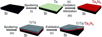
The procedure used to synthesize Ta3N5 by thin film transfer is presented in Fig. 1. Single-crystalline Si wafers (Nilaco Co.) were cut into specimens with dimensions of 1 × 1 cm. These Si substrates were then treated by sequential sonication in acetone, 2-propanol and Milli-Q water (18.2 mΩ cm), and the cleaned Si substrates were directly used, without HF etching to remove the surface native SiO2. Thin Ta films, with thicknesses ranging from 150 to 800 nm, were deposited on these Si substrates by radio-frequency (RF) magnetron sputtering (ULVAC, MNS-2000-RFG3) at a substrate temperature of 500 °C. The working pressure and the output power of the Ar plasma during this process were 1.0 × 10⁻¹ Pa and 100 W, respectively. The deposition rate of the Ta film was 25 nm min−1. The resulting Ta/Si samples were oxidised in a muffle furnace at 700 °C for 2 h to form Ta2O5 films, and these Ta2O5/Si specimens were subsequently nitrided in a flow of gaseous NH3 (100 sccm) at 900 °C for 2 h to produce Ta3N5 thin films on the Si substrates. Ta (150 nm) and Ti (approximately 5 μm) layers were then sputtered on top of the as-nitrided Ta3N5 thin films. In some cases, the Ta layer was replaced with Nb, Ti, Zr (containing 4.5% Hf) or Mg and different contact materials were investigated, as described in the ESI.† The Ta3N5/Ta/Ti films could be completely peeled away from the Si substrates by mechanical exfoliation. The transferred films were cleaned with an HF/HNO3/H2O (1/2/7, v/v) solution for 10 s. Subsequently, the back side of each Ta3N5/Ta/Ti sample was attached to a glass plate with carbon tape and connected to an electrical wire using indium solder. The electrode area exposed to the electrolyte solution was defined by applying a water-proof epoxy resin, and the typical exposed electrode area was approximately 0.2 cm2.A layer of Co(OH)x was deposited on the surface of each Ta3N5 photoelectrode prior to the photoelectrochemical (PEC) measurements. An aqueous 2.5 mL NaOH (50 mM) solution was added to 10 mL of an aqueous Co(NO3)2 (6.3 mM) solution, and the as-prepared Ta3N5 photoelectrode was immersed in the mixture for 1 h. As the initial blue solution gradually transitioned to a yellow colloidal suspension, a thin layer of Co(OH)x was formed on the surface of the electrode.
Characterization
Scanning electron microscopy (SEM; S-4700, Hitachi), scanning transmission electron microscopy and transmission electron microscopy (STEM, TEM; JEM-2800, JEOL) in conjunction with energy-dispersive X-ray spectroscopy (EDS; EX-24055JGT, JEOL) were used to characterise the morphologies and cross-sectional structures of the Ta3N5 thin films. X-ray diffraction (XRD; Rigaku Ultima III) patterns were acquired using Cu Kα radiation (λ = 0.15405 nm, 40 mV and 40 mA) and X-ray photoelectron spectroscopy (XPS; JEOL, JPS-90SX) was performed with Mg Kα radiation (8 kV and 10 mA).Photoelectrochemical measurements
The PEC properties of the Ta3N5 photoanodes were assessed in a three-electrode cell controlled by a potentiostat (Hokuto Denko, HSV-110). An Ag/AgCl (in saturated KCl aq.) electrode and a Pt wire were used as the reference and counter electrodes, respectively. The potential against the Ag/AgCl reference electrode (EAg/AgCl) was converted to the potential with respect to a reversible hydrogen electrode (ERHE) using the Nernst equation below.| ERHE = EAg/AgCl + 0.197 V + 0.059 × pH | (1) |
PEC measurements were performed in an aqueous solution of potassium phosphate (KPi, 0.5 M, pH 13) under a simulated AM 1.5G light source (San-EI Electric, XES-40S2-CE). The H2 and O2 gas yields from the counter electrode and a Ta3N5 photoanode held at 1.23 V vs. RHE were accumulated in an air-tight, three-electrode PEC cell and quantified using a micro gas chromatograph (Agilent, 3000A, Micro GC).
Results and discussion
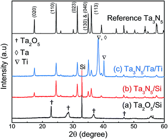
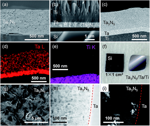
Fig. 2 presents XRD patterns for the thin film samples before nitridation, after nitridation, and after film transfer. Fig. 2(a) demonstrates that a crystalline Ta2O5 film was formed by oxidising the metallic Ta film at 700 °C, while Fig. 2(b) shows that a Ta3N5 film with an orthorhombic phase was formed on the Si substrate by nitridation at 900 °C. The crystalline Ta3N5 films were evidently preserved during the film transfer process (Fig. 2(c)). Ta2N and Ta5N6, which are both typical impurity phases in Ta3N5 films grown on Ta metal substrates,26,27 were not observed in our Ta3N5 films having thicknesses of 570, 1120, and 1620 nm, as shown in Fig. S1 in the ESI.† This suggests that reduction of the Ta3N5 phase during the nitridation process was inhibited owing to the absence of the underlying Ta metal. Complete transformation to Ta3N5 was achieved even in the case of the especially thick Ta3N5 films (>1000 nm). This was likely due to the formation of a porous structure that facilitated penetration of N or NH species throughout the film.Fig. 3(a) shows a cross-sectional SEM image of a Ta3N5 film on a Si substrate. This porous Ta3N5 film was formed by nitridation as the three O2− anions in the original Ta2O5 film were replaced by two N3− anions. From the cross-sectional images (Fig. 3(b) and (c)), it is evident that the thickness of the Ta3N5 film (570 nm) remained unchanged during the film transfer process. The multi-layer Ta3N5/Ta/Ti structure was further confirmed by the cross-sectional EDS maps presented in Fig. 3(d) and (e). Because the sputtered Ta/Ti layer resulted in rigid contact with the Ta3N5 layer, the Ta3N5 film was readily exfoliated from the Si substrate without damaging the layered structure of the Ta3N5/Ta/Ti film. However, Ta3N5 films thinner than 300 nm could not be peeled away from the Si substrate without breaking. It is believed that the presence of significant porosity at the film/substrate interface plays a key role in successful film transfer, given the correlation between the porosity and thickness of Ta3N5 thin films.19 The metallic Ta and Ti layers acted as a back contact and a conductive support for the Ta3N5 films, respectively. The transferred Ta3N5 film was flexible (Fig. 3(f)) and had a rough surface originating from the porosity of the Ta3N5 (Fig. 3(g)). XPS analysis of the Ta3N5 films before and after transfer (Fig. S2†) revealed that no Si species were present on the surface of the Ta3N5 film after thin film transfer. This result demonstrates a lack of Si diffusion into the bulk of the Ta3N5 film, owing to the stability of the Si substrates during the high temperature nitridation.
In order to examine the structural properties of the Ta3N5 film, a dark-field (DF) STEM image (Fig. 2(h)) of a cross section close to the Ta3N5/Ta interface was acquired. The bright contrast in this DF-STEM image indicates a highly porous structure for the transferred Ta3N5 film. The average size of the pores between the Ta3N5 grains was approximately 20 nm, and thus was likely responsible for the high surface area of the Ta3N5 photoelectrodes. The average grain sizes of Ta3N5 crystals were estimated from the zone-axis TEM image (Fig. 2(i)) to be in the range of 20 to 50 nm, a value that is much smaller than the film thickness (570 nm). The TEM fast Fourier transform (FFT) diffraction patterns also demonstrate disorder in the arrangement of the Ta3N5 grains (Fig. S3†). Hence, a number of grain boundaries were present in the Ta3N5 film. However, the thin film was in intimate contact with the polycrystalline Ta layer prepared by magnetron sputtering. Owing to the matching of the work function of metallic Ta (4.3 eV)29 and the flat band potential of the Ta3N5 electrode (0.02 V vs. RHE, Fig. S4†), an ohmic contact was expected to be present at the Ta3N5/Ta interface. As a result, the energy barrier for the transport of photogenerated electrons across the Ta3N5/Ta interface was minimized.
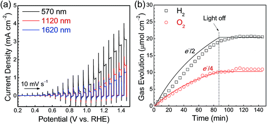
Current–potential curves for Ta3N5 photoanodes with film thicknesses of 570, 1120 and 1620 nm were obtained under simulated AM 1.5G light and are presented in Fig. 4(a). A photocurrent density of 2.0 mA cm−2 at 1.23 V vs. RHE was observed in the case of the Ta3N5(570 nm)/Ta/Ti photoelectrode modified with a cobalt-based oxygen-evolution catalyst. The faradaic efficiency for PEC water oxidation reaction was determined by quantifying the O2 evolved at the Ta3N5/Ta/Ti photoanode held at 1.23 V vs. RHE and the H2 evolved at the Pt counter electrode by gas chromatography (Fig. 4(b)). The faradaic efficiency of almost unity indicates that the photoanodic current generated by the Ta3N5 photoelectrode is primarily attributable to the O2 evolution process. The incident photon-to-current conversion efficiency (IPCE) spectrum (Fig. S5†) demonstrates that the Ta3N5 film photoanodes were capable of utilising visible light up to 600 nm, corresponding to the bandgap of Ta3N5 (2.1 eV), for PEC water oxidation. However, because of the porous nature of the Ta3N5 films, the photoelectrode surface was not fully covered with the Co(OH)x layer (Fig. S6†). As a result, the O2 evolution rate decreased gradually over time owing to the photocorrosion of the Ta3N5 films.
A significant decrease in the photocurrent density was associated with increases in the film thicknesses of the Ta3N5 photoelectrodes. The probability of charge carrier recombination in thicker Ta3N5 films is expected to be higher, given the large number of grain boundaries acting as electron–hole recombination centres and the long diffusion distances for both holes and electrons. It should be noted that Ta3N5 films thinner than 300 nm could not be prepared by film transfer from Si substrates as described above.19 Therefore, a film thickness of approximately 600 nm was the optimum value for the Ta3N5 photoanodes prepared by thin film transfer. This thickness is consistent with the layer thickness reported for Ta3N5 photoelectrodes with exhibiting superior PEC performance.19,24
The thin film transfer method allows tuning of the thickness of the Ta3N5 film to arbitrary values above approximately 550 nm. Another and potentially more important feature of the film transfer technique is the possibility of obtaining the desired multi-layer structure in the Ta3N5 film. It is conceptually possible to introduce doping, catalytic, protective, and/or sacrificial template layers at the front and/or rear sides of the Ta3N5 film by depositing such functional layers before and/or after formation of either the Ta or Ta2O5 layers. It is also feasible to use materials other than Ta, such as metals, sulphides, and nitrides, as contact layers after the nitridation. As an example, current–potential curves for Ta3N5 photoelectrodes with different metallic contact layers (Ta, Nb, Ti, Zr and Mg) are shown in Fig. 5(a). It was found that Ta3N5 photoelectrodes with Ta and Nb back contacts showed higher photocurrents than those with Mg and Zr back contacts although all the metallic layers were expected to form an ohmic contact with the Ta3N5 films. A Mg or Zr contact layer with small work function (Table S1 in ESI†) was probably too sensitive to oxygen to form an ideal ohmic junction, resulting in a poor PEC performance. In addition, NbNx, TiNx and CdS were introduced as back contact materials for Ta3N5 photoelectrodes (Fig. 5(b) and S7†). A Ta3N5/NbNx/Ta photoelectrode with a NbNx back contact generated a higher current density (3.5 ± 0.2 mA cm−2 at 1.23 V vs. RHE) than a Ta3N5/Ta photoelectrode (2.2 ± 0.2 mA cm−2), as shown in Fig. S8,† while TiNx and CdS back contacts lowered the PEC activity. The photocurrent of the Ta3N5/NbNx/Ta photoanode decayed with time, similarly to the Ta3N5/NbNx/Ta photoanode, because the interlayer did not suppress photocorrosion of the Ta3N5 surface. In addition, the effects of the back contact materials on the properties of the Ta3N5 films are not fully understood at present. However, it is clear that certain back contact materials can promote PEC oxygen evolution on Ta3N5 thin films. In future work, this film transfer process is expected to allow clarification of the promotional effect of interlayers on the PEC properties of Ta3N5 films by taking advantage of the controllability of the layered structure.
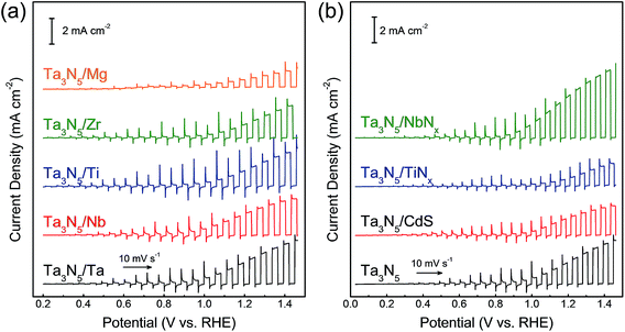 | ||
| Fig. 5 Current–potential curves obtained from Ta3N5 photoanodes with different back contact layers. (a) Ta3N5/M/Ti (M = Ta, Nb, Ti, Zr and Mg), and (b) Ta3N5/N/Ta/Ti (N = NbNx, TiNx and CdS). | ||
Conclusions
A thin film transfer method for the fabrication of Ta3N5 thin films having different thicknesses and back contact layers has been demonstrated. The inertness of the Si substrates allowed the synthesis of pure, crystalline Ta3N5 films via the thermal nitridation of sputtered Ta films, and also resulted in weak adhesion at the Ta3N5/Si interface that promoted the film transfer process. This new preparation method allows optimization of the PEC performance of Ta3N5 thin film photoanodes by controlling the film thickness. Ta3N5(570 nm)/Ta/Ti photoanodes generated a photocurrent of 2.0 mA cm−2 at 1.23 V vs. RHE under simulated AM 1.5G light, while thicker films produced lower photocurrents because of the longer charge carrier migration distances and the greater concentration of grain boundaries. The photocurrent at 1.23 V vs. RHE could be further enhanced to 3.5 mA cm−2 by modification of the back contact layer applied to the transferred Ta3N5 film.This film transfer procedure circumvents current strict requirements for the conductive substrates that can be employed during vigorous annealing treatments, enabling the preparation and the transfer of semiconductor thin films from various inert substrates. Therefore, the new fabrication strategy presented herein has the potential to allow the preparation of thin film photoelectrodes composed of materials such as α-Fe2O3, BiVO4 and BaTaO2N for applications in PEC water splitting and/or PEC solar cells.
Acknowledgements
This work was financially supported by Grants-in-Aid for Specially Promoted Research (No. 23000009), for Young Scientists (A) (No. 15H05494) and Young Scientists (B) (No. 5K17895) of Japan Society for the Promotion of Science (JSPS). This work was partly supported by the Artificial Photosynthesis Project (ARPChem) of the New Energy and Industrial Technology Development Organization (NEDO). Part of this work was conducted at the Research Hub for Advanced Nano Characterization at the University of Tokyo, under the support of the “Nanotechnology Platform” (project No. 12024046) of the Ministry of Education, Culture, Sports, Science and Technology (MEXT), Japan. The authors thank Dr Qian Wang, Dr Miao Zhong, Dr Taro Yamada and Mr Yutaka Sasaki in the University of Tokyo for SEM characterisation and discussions.References
- M. Grätzel, Nature, 2001, 414, 338–344 CrossRef PubMed.
- A. Fujishima and K. Honda, Nature, 1972, 238, 37–38 CrossRef CAS PubMed.
- A. J. Nozik, Annu. Rev. Phys. Chem., 1978, 29, 189–222 CrossRef CAS.
- M. G. Walter, E. L. Warren, J. R. McKone, S. W. Boettcher, Q. Mi, E. A. Santori and N. S. Lewis, Chem. Rev., 2010, 110, 6446–6473 CrossRef CAS PubMed.
- T. Hisatomi, J. Kubota and K. Domen, Chem. Soc. Rev., 2014, 43, 7520–7535 RSC.
- M. Zhong, Y. Ma, P. Oleynikov, K. Domen and J.-J. Delaunay, Energy Environ. Sci., 2014, 7, 1693–1699 CAS.
- K. Ueda, T. Minegishi, J. Clune, M. Nakabayashi, T. Hisatomi, H. Nishiyama, M. Katayama, N. Shibata, J. Kubota, T. Yamada and K. Domen, J. Am. Chem. Soc., 2015, 137, 2227–2230 CrossRef CAS PubMed.
- T. Minegishi, N. Nishimura, J. Kubota and K. Domen, Chem. Sci., 2013, 4, 1120–1124 RSC.
- H. X. Dang, N. T. Hahn, H. S. Park, A. J. Bard and C. B. Mullins, J. Phys. Chem. C, 2012, 116, 19225–19232 CAS.
- S. Khan, M. J. M. Zapata, M. B. Pereira, R. V. Goncalves, L. Strizik, J. Dupont, M. J. L. Santos and S. R. Teixeira, Phys. Chem. Chem. Phys., 2015, 17, 23952–23962 RSC.
- C. Wang, T. Hisatomi, T. Minegishi, Q. Wang, M. Zhong, M. Katayama, J. Kubota and K. Domen, J. Phys. Chem. C, 2016 DOI:10.1021/acs.jpcc.5b11564.
- G. J. Liu, J. Y. Shi, F. X. Zhang, Z. Chen, J. F. Han, C. M. Ding, S. S. Chen, Z. L. Wang, H. X. Han and C. Li, Angew. Chem., Int. Ed., 2014, 53, 7295–7299 CrossRef CAS PubMed.
- M. X. Li, W. J. Luo, D. P. Cao, X. Zhao, Z. S. Li, T. Yu and Z. G. Zou, Angew. Chem., Int. Ed., 2013, 52, 11016–11020 CrossRef CAS PubMed.
- D. Yokoyama, H. Hashiguchi, K. Maeda, T. Minegishi, T. Takata, R. Abe, J. Kubota and K. Domen, Thin Solid Films, 2011, 519, 2087–2092 CrossRef CAS.
- M. Higashi, K. Domen and R. Abe, J. Am. Chem. Soc., 2013, 135, 10238–10241 CrossRef CAS PubMed.
- J. Seo, T. Takata, M. Nakabayashi, T. Hisatomi, N. Shibata, T. Minegishi and K. Domen, J. Am. Chem. Soc., 2015, 137, 12780–12783 CrossRef CAS PubMed.
- W. J. Chun, A. Ishikawa, H. Fujisawa, T. Takata, J. N. Kondo, M. Hara, M. Kawai, Y. Matsumoto and K. Domen, J. Phys. Chem. B, 2003, 107, 1798–1803 CrossRef CAS.
- M. Higashi, K. Domen and R. Abe, Energy Environ. Sci., 2011, 4, 4138–4147 CAS.
- B. A. Pinaud, P. C. K. Vesborg and T. F. Jaramillo, J. Phys. Chem. C, 2012, 116, 15918–15924 CAS.
- A. Dabirian and R. van de Krol, Chem. Mater., 2015, 27, 708–715 CrossRef CAS.
- A. Ziani, E. Nurlaela, D. S. Dhawale, D. A. Silva, E. Alarousu, O. F. Mohammed and K. Takanabe, Phys. Chem. Chem. Phys., 2015, 17, 2670–2677 RSC.
- J. M. Morbec, I. Narkeviciute, T. F. Jaramillo and G. Galli, Phys. Rev. B, 2014, 90, 155204 CrossRef.
- G. Liu, S. Ye, P. Yan, F. Xiong, P. Fu, Z. Wang, Z. Chen, J. Shi and C. Li, Energy Environ. Sci., 2016, 9, 1327–1334 CAS.
- Y. Li, L. Zhang, A. Torres-Pardo, J. M. González-Calbet, Y. Ma, P. Oleynikov, O. Terasaki, S. Asahina, M. Shima, D. Cha, L. Zhao, K. Takanabe, J. Kubota and K. Domen, Nat. Commun., 2013, 4, 2566 Search PubMed.
- C. Zhen, L. Wang, G. Liu, G. Q. Lu and H.-M. Cheng, Chem. Commun., 2013, 49, 3019–3021 RSC.
- B. A. Pinaud, A. Vailionis and T. F. Jaramillo, Chem. Mater., 2014, 26, 1576–1582 CrossRef CAS.
- Y. Li, T. Takata, D. Cha, K. Takanabe, T. Minegishi, J. Kubota and K. Domen, Adv. Mater., 2013, 25, 125–131 CrossRef CAS PubMed.
- T. Nobuzo, Jpn. J. Appl. Phys., 1971, 10, 248–259 CrossRef.
- H. L. Skriver and N. M. Rosengaard, Phys. Rev. B: Condens. Matter Mater. Phys., 1992, 46, 7157–7168 CrossRef CAS.
Footnote |
| † Electronic supplementary information (ESI) available. See DOI: 10.1039/c6sc01763k |
| This journal is © The Royal Society of Chemistry 2016 |

