
Synergistic crucible design and thermal-flow management for enhanced 4-inch AlN single crystal PVT growth: a combined numerical and experimental investigation
Wenliang
Li
 ab,
QianLing
Liu
ab,
Jun
Tan
ab,
Guangze
He
ab,
Yingmin
Wang
cd,
Zhenhua
Sun
ab,
Baikui
Li
ab and
Honglei
Wu
*ab
ab,
QianLing
Liu
ab,
Jun
Tan
ab,
Guangze
He
ab,
Yingmin
Wang
cd,
Zhenhua
Sun
ab,
Baikui
Li
ab and
Honglei
Wu
*ab
aState Key Laboratory of Radio Frequency Heterogeneous Integration (Shenzhen University), College of Physics and Optoelectronic Engineering, Shenzhen University, Shenzhen, 518060, China. E-mail: hlwu@szu.edu.cn
bKey Laboratory of Optoelectronic Devices and Systems of Ministry of Education and Guangdong Province, College of Physics and Optoelectronic Engineering, Shenzhen University, Shenzhen, 518060, China
cThe 46th Research Institute, China Electronics Technology Group Corporation, Tianjin, 300220, China
dKey Laboratory of Advanced Semiconductor Materials of CTEC, Tianjin, 300220, China
First published on 25th March 2025
Abstract
High-quality, large-diameter aluminum nitride (AlN) single crystals are essential for advanced electronic and optoelectronic applications. However, their physical vapor transport (PVT) growth remains challenging due to complex thermal-flow dynamics and crucible design limitations. In this study, we comprehensively investigate the synergistic optimization of crucible geometry and thermal-flow management on a VR-PVT crystal growth platform. Numerical simulations reveal that positioning the seed crystal at 35–45% of the main heater's height stabilizes the growth rate, while refined crucible design and optimized vapor pathways ensure a uniform thermal-flow field for sustained growth. Experimental validation demonstrates the efficacy of our approach by producing AlN ingots exceeding 4 inches in diameter. X-ray diffraction (XRD) analysis shows that the full width at half maximum (FWHM) of the rocking curve for the (0002) plane ranges from 277 to 446 arcsec. Raman spectroscopy further indicates that the FWHM of the E2 (high) phonon mode falls between 7.41 and 7.62 cm−1. Both measurements confirm that the synthesized AlN crystal exhibits good uniformity. These results provide valuable process insights and establish a scalable framework for PVT-based synthesis of high-quality AlN single crystals.
Introduction
Aluminum nitride (AlN) is a wide-bandgap semiconductor (6.2 eV) distinguished by its high thermal stability, large breakdown electric field (∼15 MV cm−1), and fast surface acoustic wave velocity.1–4 These attributes make AlN promising for high-temperature, high-frequency, and high-power electronic devices, especially as substrates for ultraviolet solid-state lasers, GaN-based high-electron-mobility transistors (HEMTs),5 and solar-blind AlGaN photodetectors.6 AlN single-crystal growth can be accomplished via hydride vapor phase epitaxy (HVPE),7,8 molecular beam epitaxy (MBE),9 metal–organic chemical vapor deposition (MOCVD),10,11 and physical vapor transport (PVT),12,13 of which PVT is currently the most established technique for synthesizing large-diameter, high-quality AlN. However, due to the demanding conditions—extremely high temperatures (2170–2570 K), long growth durations (>100 h), and tight thermal stability requirements—PVT growth optimization through purely experimental means is expensive and time-consuming. Consequently, numerical simulation has become an indispensable tool for improving the growth process.14A standard PVT system comprises a resistive heater, multilayer insulation, and a sealed crucible containing both the AlN source and the seed crystal, wherein radiation dominates heat transfer. The crystal morphology and defect density are impacted by seed polarity, source sublimation rate, and vapor transport efficiency, while thermodynamic parameters depend on crucible geometry, insulation configuration, and the height of the source powder. Excessive axial temperature gradients can lead to radial differences in growth rate, which promote dislocation proliferation. Because direct in situ observation under extreme temperatures is not feasible, computational fluid dynamics (CFD)-based simulations have become critical for elucidating growth mechanisms and optimizing process conditions.
Substantial progress has been made in multiphysics modeling of AlN PVT. Karpov et al. developed an initial model incorporating gas diffusion, natural convection, and surface reaction kinetics, highlighting the influence of nitrogen partial pressure on crystal morphology.15 Liu et al. predicted bulk growth rates by applying global mass-balance equations.16 More recently, Wu et al. compared the thermal field characteristics of resistive vs. induction heating, demonstrating contrasting axial temperature gradients.17 Wang et al. employed 3D finite-element modeling to quantify how Stefan flow and buoyancy jointly influence mass transport.18 Nonetheless, most prior work has focused on temperature or stress fields, and comparatively little attention has been paid to the dynamic evolution of the V/III ratio (i.e., the N/Al atomic ratio) and its effects on crystal quality.
This study addresses the critical role of changes in the thermal-flow field and gaseous substances in crystal uniformity and defect formation during AlN growth. Combining numerical simulations with experimental validation, we systematically examine how crucible design, positional adjustments, and rear-structure modifications affect the thermal-flow field and growth uniformity. Our findings provide fundamental insights for optimizing thermal field design and growth conditions for large-diameter AlN crystals grown by PVT.
Experiment
Crystal growth numerical simulation configurations
AlN single crystals were grown in-house using a resistively heated PVT system developed by our laboratory. The core reactor includes a tungsten heating element, multilayer insulation, a tungsten crucible, and an AlN source-seed assembly (Fig. 1(a)).19 During a typical growth cycle, the AlN source material undergoes thermal decomposition in a high-temperature region (T_source = 2520–2620 K): and the Al- and N-containing gas-phase species migrate via thermodynamic forces toward the seed crystal. Optimized process parameters include ≥99.9995% purity for the nitrogen environment, a system pressure of 0.3–0.8 atm, and a growth duration of 10–80 h. | ||
| Fig. 1 (a) Schematic diagram of the interior of crystal growth (the red coordinate scale indicates the relative position of the seed crystal with respect to the center of the main heater). (b) The thermal field distribution within the crucible at 10% of the main heater's center position for the seed crystal. | ||
Global thermal-field simulations were performed using the STR Company's VR-PVT multiphysics platform, which constructs a three-dimensional asymmetric model based on finite-element formulations. By simultaneously solving the Navier–Stokes equations and radiative heat-transfer equations, the software accurately predicts temperature gradients (±5 °C deviation) and mass-transport profiles within the growth chamber. A coupled thermal-flow field model was employed to analyze how axial temperature gradients and natural convection intensity affect the crystal-growth interface. Iterative calculations were used to optimize the crucible's axial position, ensuring stable growth on the seed-crystal surface.
Geometric model and simulation parameters of thermal field
Because of the reactor's rotational symmetry, two-dimensional axisymmetric modeling was employed for the numerical analysis. Nonessential features that have negligible effects on thermal distribution—such as thermocouple ports or minor mechanical gaps—were omitted, while key components (the cylindrical furnace, heaters, crucible, and surrounding insulation) were retained. The heater was simplified as a cylindrical tube with equivalent volume, and its power input was used directly in simulations. The insulation was also simplified to an equivalent cylindrical volume, ensuring that the system matched the experimental conditions for AlN crystal growth at a given power setting.Resistive heating was utilized; control of heater power regulated system temperature, while adjusting the crucible's position further shaped the internal temperature field. Because AlN growth by PVT occurs at high temperatures, heat conduction, convection, and radiation dominate energy transfer. In the PVT process, crystal growth depends on the combined effects of heat conduction, convection, and radiation at high temperatures. Firstly, the heat conduction in the crystal-growth region can be described by Fourier's law:
| q = −k∇T | (1) |
For the convective heat transfer in the furnace, Newton's law of cooling is used to describe the convective transfer of heat flux:
| q = hA(Ts − T∞) | (2) |
As an important heat-transfer mechanism in high-temperature systems, radiation follows the Stefan–Boltzmann law:
| q = εσA(Ts4 − T∞4) | (3) |
During the growth of AlN crystals by the PVT method, mass transport mainly involves the diffusion and convection of Al and N atoms in the gas phase to the growth interface. This process can be described by Fick's first law for gas-phase diffusion:
| J = −D∇C | (4) |
In addition, gas-phase transport is also affected by convection. The total flux of the mass-transfer process can be described by the following formula:
| J = −D∇C + υC | (5) |
The growth rate of AlN crystals is controlled by multiple factors, including the temperature field and mass transport. The dependence of the growth rate on temperature can be described by the Arrhenius equation:
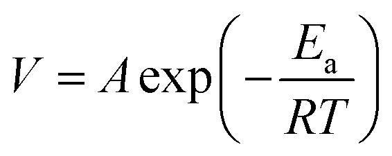 | (6) |
By simultaneously solving these equations, the VR-PVT platform accurately captures the thermal profile and mass-transport behavior during AlN PVT growth, thereby facilitating reliable process optimization. The AlN boules were processed via diamond wire sectioning and subsequently subjected to sequential surface treatments comprising grinding, mechanical polishing, and chemical polishing to attain specular surfaces. Phase identification and crystallinity assessment were implemented through high-resolution X-ray diffraction (PANalytical X'Pert PRO system) employing monochromatic Cu Kα radiation (λ = 1.5406 Å). Raman spectroscopic analysis was conducted using a confocal micro-Raman system (Horiba LabRAM HR800) config.d with an 1800 grooves per mm diffraction grating, employing 532 nm wavelength excitation under ambient conditions. For mechanical testing, a Nano Indenter G200 nano-mechanical probing system, manufactured by Agilent Technologies, was used.
Results and discussion
Effect of crucible position on the internal thermal field
The relative position of the crucible in the thermal field significantly affects the thermal-field distribution inside the crucible, which in turn influences the transport of gas-phase substances after the decomposition of aluminum nitride materials. The gas-phase substances are transported inside the crucible under the combined control of the thermal field and the flow field. The distribution ratio of N and Al atoms affects the uniformity of the crystal-growth process. As shown in Fig. 1(a), in the simulation, the center point of the main heater was taken as the reference position. With the position of the heater unchanged, the crucible was moved upward by different distances, and the position was represented by the percentage of the relative height with respect to the main heater. During the simulation process, a global temperature-field simulation was carried out. To ensure a positive-temperature-field distribution at the crystal-growth position, the crystal-growth crucible was located in the upper part of the main heater. In the simulation, 8 datasets were set at relative distances of every 5% to analyze the thermal-field conditions at different positions.The thermal field distribution when the relative position of the seed crystal to the main heater is 10% is shown in Fig. 1(b). The position of the crucible has a great impact on the thermal-field distribution inside the crucible. Referring to the actual parameters of the 4-inch AlN crystal-growth furnace of the research group, the power of the heater and the parameters of the insulation layer were set. During the simulation process, the crucible position was adjusted to keep the temperature at the seed-crystal position within the range of 2500–2560 K. When the crucible is closer to the center point of the heater, the temperature at the seed-crystal position is higher. When the crucible moves towards the upper edge of the crucible, the radial temperature difference at the seed-crystal position gradually increases. When the seed-crystal is 35% away from the center point of the heater, the radial temperature difference reaches a maximum of 5.4 K, as shown in Fig. 2(a). When the crucible position is further increased, due to the constraints of the main-heater edge and the top-heater on the seed-crystal, the radial temperature difference at the seed-crystal position decreases.
 | ||
| Fig. 2 (a) Temperature stability at the seed-crystal position with different crucible positions; (b) axial temperature difference at the seed-crystal position with different crucible positions; (c) radial temperature difference at the seed-crystal position with different crucible positions; (d) initial-stage growth rate at the seed-crystal position with different crucible positions. | ||
Fig. 2(d) indicates that at the early growth stage, the closer the crucible is to the top of the main heater, the higher the growth rate. Within the 35–45% interval, initial growth rates are nearly the same. However, without further optimization, sublimation primarily occurs at the source sidewalls and crucible bottom, resulting in a notably higher growth rate at the seed periphery than at the crystal center. Around 20–30 mm in radial distance, the growth rate drops and yields a “concave” morphology. As growth proceeds, the growth rate in the 20–30 mm region increases, while that in the 30–50 mm region decreases.
A 45-hour simulated growth run was conducted without additional optimization to capture long-term dynamics. Fig. 3 shows the crystal growth rate and surface morphology at different times. Early in the process, a larger axial temperature gradient correlates with higher local growth rates (25–92 μm h−1). The radial trend shows slower growth in the center and faster growth at the edges. Over time, as sublimation at the sidewalls declines, edge growth slows, creating a new inflection point near the boundary. After 30 hours, for low crucible positions (10–25%), the surface near r < 30 mm is still concave, while 30–50 mm shows a minor protrusion. At higher crucible positions, the crystal transitions to a deeper “center-concave” shape with a noticeable edge protrusion. Such inconsistent radial growth often introduces lattice misalignments and creates dislocation clusters.
 | ||
| Fig. 3 Growth rates and outcomes of crystals at different crucible positions (a) growth rate at 15 hours of crystal growth (b) growth rate during the initial stage at 30 hours of crystal growth (c) results after 30 hours of crystal growth (d) results after 45 hours of crystal growth. | ||
Attaining a large, high-quality AlN crystal requires uniform growth across the seed surface. A common metric for growth uniformity is comparing the center vs. edge thickness after prolonged growth. Our simulations show that, without further crucible or flow-field optimization, the unoptimized system leads to poor long-term uniformity.
Thermal-flow field optimization in the growth system
To enhance growth uniformity, we modified the microstructure of the crucible and its internal vapor flow paths. For 4-inch AlN crystals grown by traditional sidewall heating, adjusting only the crucible position is insufficient to solve morphological issues. Because sidewall radiation and conduction heat the crucible periphery, sublimation predominantly occurs near the sidewall, causing a faster deposition at the seed edge (“concave center”). To mitigate this, we designed three new crucible geometries to modulate the thermal-flow field, seeking a more uniform long-term growth.Crucible geometry is the structural foundation for achieving uniform growth. It governs thermal and flow conditions within the PVT environment. Based on optimal parameters identified in the preceding analysis, three microstructural variants—structures A, B, and C—were proposed. Fig. 4 contrasts them with the original design. Structure A features a thin ring of varying diameters, structure B adds a narrow “separation ring” at ∼30–40 mm, and structure C includes an air-gap layer behind the seed crystal. We focus primarily on seed-zone thermal effects here.
 | ||
| Fig. 4 Structural diagrams of different micro-designs: (a) original structure, (b) structure A, (c) structure B, (d) structure C. Diagrams for different micro-designs: (e) temperature distribution at the seed crystal location, (f) axial temperature gradient at the seed crystal location, (g) initial-stage growth rate at the seed crystal location, (h) crystal morphology at the seed crystal location after 30-hour growth. | ||
The radial temperature distributions, growth rates, and growth results of different crucible designs are shown in Fig. 4. As can be seen from Fig. 4(a), compared with the original structure, structure A acts as a local insulation layer. The temperature at the edge of the seed crystal increases significantly, and the temperature at the center of the seed crystal also increases slightly, resulting in an increase in the radial temperature difference at the seed-crystal position. Since structure B is a narrow separation-ring structure with a certain height, these narrow rings can reduce the thermal radiation of the heater, causing the overall temperature at the seed-crystal position to be slightly lower than that of the original structure. Notably, in the area covered by the separation rings, at the 30–40 mm position of the seed crystal, a more significant temperature drop occurs. Structure C constructs an air-layer structure, forming a closed insulation-layer structure. Under this structure, the temperature at the seed-crystal position increases by approximately 11 K, while the temperature difference does not increase significantly.
Fig. 4(b) shows the approximate result diagram of the temperature gradient between the seed-crystal position and the top of the material during the initial growth stage. On the premise that the simulation variable is only the back-layer structure, the temperature conditions at the same diameter of the seed crystal and the top of the material are selected, and an approximate result diagram of the temperature-gradient change is obtained through curve fitting and processing. Combining Fig. 4(b–d), structure A, by adjusting the temperature of the seed crystal and the temperature gradient between the crystal and the material, initially achieves a higher growth rate at the middle position of the seed crystal than at the edge. However, there are still changes in the growth-rate trend near a diameter of 10 mm and an increase in the growth rate at a diameter of 45–50 mm. Further optimization of the structure and the flow field is required to achieve consistent growth-rate trends and obtain a “nearly flat and slightly convex” growth morphology for the crystal. Structure B constructs a “low-temperature zone” between the two narrow rings, increasing the temperature gradient in the “low-temperature zone”. Driven by thermodynamics, the crystal growth rate in the “low-temperature zone” is 16% higher than that in the unoptimized case. Ultimately, compared with the unoptimized case, the crystal thickness in the “low-temperature zone” increases. The temperature-gradient situation and the growth thickness show similar trends. Due to factors such as the flow field, the initial growth rate has the same change trend as the above-mentioned two in the radius range of 0–40 mm, but the change trend is different in the 40–50 mm range. Therefore, optimizing the flow-field conditions inside the crucible is another effective way to control the consistency of the growth trend during the growth cycle.
None of these single modifications can alone ensure ideal uniformity over prolonged growth. By refining both crucible geometry and internal flow, one can adjust vapor transport pathways and reduce edge-centric deposition. Early in the growth of large-diameter AlN, the crystal often starts out “center-concave”, flattening or slightly doming after tens of hours. Such morphological shifts generate stress that can lead to cracking. Under stable thermal-field conditions, by changing the shape of the material, the transport of Al and N atoms inside the crucible can be altered to achieve the purpose of controlling the uniform growth of the crystal. In the simulation of this study, by changing the height D1 from the material to the seed crystal and the distance D2 from the material to the side-wall, typical parameter information was selected for analysis.
The crystal growth under different D1 values is shown in Fig. 5. As the distance between the material and the seed crystal increases, the space inside the crucible expands, and the radiant heat received by the seed crystal from the crucible wall also increases, causing the temperature at the seed-crystal position to rise. In the closed and constant-pressure environment inside the crucible, according to the ideal gas law
| PV = nRT | (7) |
 | ||
| Fig. 5 (a) Conditions inside the crucible (b) temperature distribution at the seed crystal position in the initial stage (c) pressure ratio of Al vapor at the seed crystal position in the initial stage (d) growth rate at the seed crystal position in the initial stage (e) results of the seed crystal growth for 30 h at different distances from the material surface. | ||
Fig. 5(e) shows the growth rate at the seed crystal position in the initial stage. The smaller the distance between the material surfaces, the larger the temperature gradient, and simultaneously, the shorter the migration path of Al atoms. Under the combined effect of the temperature gradient and the migration path, the growth rates at the center and the edge of the crystal are higher, while that at the middle position is lower. Thus, the crystal still exhibits a “concave-in-the-middle” morphology. However, when the distance between the material surfaces is ≥11 mm, in addition to the “concave-in-the-middle” morphology, due to the existence of the growth rate inflection point, a “protrusion” appears at the edge of the crystal.
After optimizing the parameter of the material-surface height, the influence of changing the distance D2 from the material to the side-wall on the crystal growth uniformity was investigated. Similar to the trend of the change in the material-surface distance, as the distance between the material and the side-wall increases, the space inside the crucible expands, and the radiant heat received by the seed crystal from the crucible wall also increases, causing the temperature at the seed-crystal position to rise, as shown in Fig. 6(a). Different distances between the material and the side-wall (2 mm, 8 mm, 14 mm, 20 mm) were set to represent the relative relationships with the diameters of the crucible and the seed crystal. Specifically, 2–20 mm respectively represent: ① 2 mm represents the limit distance for the transport of Al and N atoms from the side-wall; ② 8 mm indicates that there is a certain distance between the material and the side-wall, and the diameter of the material is slightly larger than that of the seed crystal; ③ 14 mm means that the diameter of the material is equivalent to that of the seed crystal; ④ 20 mm represents that the diameter of the material is slightly smaller than that of the seed crystal. A 30 h crystal growth experiment was carried out through simulations under these four conditions using the VR-PVT AlN software.
 | ||
| Fig. 6 Simulation of crystal growth states with different distances between the material and the side-wall: (a) temperature distribution at the seed crystal position (b) pressure ratio of Al vapor (c) situation of the Stefan flow at the seed crystal position in the initial stage (d) results of seed crystal growth for 30 h at different distances from the material surface. | ||
As the distance between the material and the side-wall increases, the space inside the crucible wall expands, and the velocity of the Stefan flow also increases with the increase in the distance between the material and the side-wall. It is noteworthy that when the distance between the material and the side-wall increases to 14 mm, that is, when the diameter of the material is equal to that of the seed crystal, during the initial growth stage, the velocity of the Stefan flow at the edge of the seed crystal is lower than that at a side-wall distance of 8 mm. As the distance between the material and the side-wall further increases, a distinct inflection point appears at a crystal radius of 35–45 mm, and this inflection point is also reflected in the growth rate graph, as shown in Fig. 6(b) and (c). Fig. 6(d) shows the results of the seed crystal growth for 30 h at different distances from the material surface. As the distance between the material and the side-wall increases, the surface undulation of the crystal becomes more significant. Moreover, as the distance between the material and the side-wall increases, the crystal morphology shows that in the range of 35–50 mm in radius, the crystal thickness shows a decreasing trend. This indicates that as the crystal growth progresses, the growth rate at the edge shows a rapid decline, ultimately leading to the appearance of a “protrusion” in the range of 35–40 mm in radius, and the vertex of this protrusion approaches the center of the crystal as the distance between the material and the side-wall increases.
During the process of optimizing the values of D1 and D2, it was found that the main sublimation regions are the central part of the top of the material and the lower part of the material near the crucible wall. By changing the shape of the material surface to reduce the deposition amount at the crystal edge, the goal of achieving uniform crystal growth can be achieved. Crystal growth is a complex process. Through simulations of the thermal and flow fields, it can be seen that single micro-structure optimization or single optimization of the thermal-flow field inside the crucible cannot yield satisfactory results. By decomposing the factors of the micro-structure and the thermal-flow field and analyzing the influence of each factor on the crystal growth results, and through the coupling of the micro-structure and the combination of the thermal-flow field, 4-inch AlN crystals with good crystallization quality and high consistency during the growth cycle can be obtained.
Crystal growth results informed by simulation
Using the in-house 4-inch AlN PVT system, we performed growth experiments guided by our simulation-optimized crucible microstructure, thermal field, and flow-field parameters. As a result, an AlN ingot with a diameter of 105 mm and a thickness of 12 mm was successfully synthesized. The ingot exhibited a “slightly convex” growth morphology [Fig. 7(a)]. The AlN ingot was subsequently sliced, ground, and polished into wafers with a thickness of 0.8 mm. | ||
| Fig. 7 Crystal growth results: (a) photograph of the synthesized 4-inch aluminum nitride ingot. (b) Photo of the cut crystal. (c) Schematic diagram illustrating sample selection positions using a nine-point test. (d) Normalized XRD test results after grinding and polishing. (e) Normalized Raman test results after grinding and polishing. (f) Hardness test results after grinding and polishing. (g) Modulus measurement results after grinding and polishing. | ||
Fig. 7(b) presents the AlN single-crystal wafers obtained from the sliced ingot, exhibiting excellent surface uniformity. This validates the high accuracy of the VR-PVT AlN simulation software in predicting the microstructure, thermal field, and flow field during the crystal growth process. Subsequent nine-point testing revealed that the full width at half maximum (FWHM) of the high-resolution X-ray diffraction (HRXRD) rocking curve for the (0002) plane ranged from 277 arcseconds (narrowest) to 446 arcseconds (widest) [Fig. 7(d)]. Similarly, the FWHM of the E2 (high) phonon mode in Raman scattering ranged from 7.41 cm−1 (narrowest) to 7.62 cm−1 (widest) [Fig. 7(e)], confirming the high crystallinity and uniformity of the AlN crystal. Mechanical testing was also conducted on the synthesized AlN crystal [Fig. 7(f) and (g)]. The results showed that the hardness of the AlN crystal ranged from 15.88 to 16.26 GPa, with an average modulus between 326.6 and 332 GPa. These measurements demonstrate the uniformity of the mechanical properties across the crystal. However, the hardness values remain lower than those reported for high-quality AlN, which may be attributed to the presence of internal defects within the material.22
Conclusions
A design framework was established for optimizing the thermal and flow fields in 4-inch AlN PVT growth. Finite-element simulations revealed that, in a conventional sidewall-heated system, elevating the crucible position initially increases radial temperature gradients at the seed, up to ∼35% of heater height, beyond which the gradient declines. Meanwhile, once the seed is placed above 35% of the heater's height, its growth rate remains nearly unchanged. We then coupled microstructural crucible design with thermal-flow field optimization to mitigate long-term nonuniformities. We found that no single structural or flow-field adjustment fully rectifies the radial inconsistencies that emerge over extended growth. Instead, effective solutions require a combined approach addressing both crucible geometry and vapor flow path. Using the optimized design, we successfully get a 105 mm wafer with excellent radial uniformity. The (0002) XRD rocking curve FWHM of the obtained wafers is as broad as 446 arcseconds, with the widest E2 (high) Raman linewidth at 7.62 cm−1, and the hardness variation across multiple points is 0.38 GPa, confirming that the prepared AlN crystals exhibit high uniformity. Overall, our work furnishes crucial theoretical and experimental insights for large-diameter, high-quality AlN crystal growth by PVT.Data availability
The data that support the findings of this study are available from the corresponding author upon reasonable request.Author contributions
H. L. Wu and W. L. Li proposed a research approach for simulating and experimentally preparing 4-inch AlN growth. Q. L. Liu and G. Z. He participated in the growth and preparation of 4-inch AlN. J. Tan and Y. M. Wang participated in growth simulation and provided parameter selection and optimization directions. B. K. Li and Z. H. Sun established and provided a material testing and characterization system. W. L. Li, Q. L. Liu, and G. Z. He participated in the characterization of the crystalline quality of the material. W. L. Li, Wu, and Z. H. Sun made contributions to the writing and editing of the manuscript.Conflicts of interest
There are no conflicts to declare.Acknowledgements
This work was supported in part by National Natural Science Foundation of China (61974094); National Key R&D Program of China (2022YFB3605303); Key Research and Development Project of Guangdong Province (2020B010169003); Science and Technology Innovation Commission of Shenzhen (JCYJ20200109105413475, JCYJ20210324093007020).References
- J. C. Yan, J. X. Wang, Y. Zhang, P. P. Cong, L. L. Sun, Y. D. Tian, C. Zhao and J. M. Li, J. Cryst. Growth, 2015, 414, 254–257 CrossRef.
- A. L. Hickman, R. Chaudhuri, S. J. Bader, K. Nomoto, L. Li, J. C. M. Hwang, H. G. Xing and D. Jena, Semicond. Sci. Technol., 2021, 36, 044001 CrossRef CAS.
- A. Yoshikawa, R. Hasegawa, T. Morishita, K. Nagase, S. Yamada, J. Grandusky, J. Mann, A. Miller and L. J. Schowalter, Appl. Phys. Express, 2020, 13, 022001 CrossRef CAS.
- Q. Zhang, G. Y. Li, X. F. Liu, F. Qian, Y. Li, T. C. Sum, C. M. Lieber and Q. H. Xiong, Nat. Commun., 2014, 5, 4953 CrossRef CAS PubMed.
- Y. Irokawa, E. A. G. Víllora and K. Shimamura, Jpn. J. Appl. Phys., 2012, 51, 040206 CrossRef.
- Z. Liu, Z. L. Fan, W. L. Li, Y. Cao, F. H. Zhang, Z. Y. Qin, Z. H. Sun, B. K. Li and H. L. Wu, CrystEngComm, 2024, 26, 6017–6024 RSC.
- X. H. Liu, J. C. Zhang, X. J. Su, J. Huang, S. N. Zheng, Y. Y. Hu, B. B. Ye, J. J. Zhao, J. F. Wang, J. P. Zhang and K. Xu, Appl. Phys. Express, 2016, 9, 045501 CrossRef.
- Y. Katagiri, S. Kishino, K. Okuura, H. Miyake and K. Hiramatu, J. Cryst. Growth, 2009, 311, 2831–2833 CrossRef CAS.
- Y. Qi, Y. Y. Wang, Z. Q. Pang, Z. P. Dou, T. B. Wei, P. Gao, S. S. Zhang, X. Z. Xu, Z. H. Chang, B. Deng, S. L. Chen, Z. L. Chen, H. N. Ci, R. Y. Wang, F. Z. Zhao, J. C. Yan, X. Y. Yi, K. H. Liu, H. L. Peng, Z. Q. Liu, L. M. Tong, J. Zhang, Y. J. Wei, J. M. Li and Z. F. Liu, J. Am. Chem. Soc., 2018, 140, 11935–11941 CrossRef CAS PubMed.
- I. Demir, H. Li, Y. Robin, R. McClintock, S. Elagoz and M. Razeghi, J. Phys. D: Appl. Phys., 2018, 51, 085104 CrossRef.
- J. Z. Hu, L. Yan, N. Zhou, Y. Chen, X. N. Yang, L. Q. Yang and S. P. Guo, J. Cryst. Growth, 2024, 626, 127463 CrossRef CAS.
- Q. K. Wang, D. Lei, J. L. Huang, X. J. Sun, D. B. Li, Z. X. Zhou and L. Wu, Front. Mater., 2023, 9, 1128468 CrossRef.
- W. H. Cao, S. Z. Wang, R. X. Yu, G. D. Wang, Y. J. Zhu, Y. Z. Wu, L. S. Lv, J. L. Liu, X. A. Xu and L. Zhang, CrystEngComm, 2024, 27, 247–255 RSC.
- Y. Yu, B. T. Liu, X. Tang, S. Liu and B. Gao, Materials, 2020, 13, 5553 CrossRef CAS PubMed.
- A. S. Segal, S. Y. Karpov, Y. N. Makarov, E. N. Mokhov, A. D. Roenkov, M. G. Ramm and Y. A. Vodakov, J. Cryst. Growth, 2000, 211, 68–72 CrossRef CAS.
- L. H. Liu and J. H. Edgar, J. Electrochem. Soc., 2002, 149, G12–G15 CrossRef CAS.
- B. Wu, R. H. Ma, H. Zhang, M. Dudley, R. Schlesser and Z. Sitar, J. Cryst. Growth, 2003, 253, 326–339 CrossRef CAS.
- G. D. Wang, L. Zhang, Y. Wang, Y. L. Shao, C. M. Chen, G. X. Liu, Y. Z. Wu and X. P. Hao, Cryst. Growth Des., 2019, 19, 6736–6742 CrossRef CAS.
- Z. Y. Qin, W. H. Chen, D. X. Deng, Z. H. Sun, B. K. Li, R. S. Zheng and H. L. Wu, Sensors, 2020, 20, 3939 CrossRef PubMed.
- W. Guo, J. Kundin, M. Bickermann and H. Emmerich, CrystEngComm, 2014, 16, 6564–6577 RSC.
- Y. X. Li and D. W. Brenner, Phys. Rev. Lett., 2004, 92, 075503 CrossRef PubMed.
- I. Yonenaga, MRS Internet J. Nitride Semicond. Res., 2002, 7, 1 CrossRef.
| This journal is © The Royal Society of Chemistry 2025 |