Engineering the surface charge states of nanostructures for enhanced catalytic performance
Yu
Bai
ab,
Hao
Huang
a,
Chengming
Wang
a,
Ran
Long
*a and
Yujie
Xiong
 *a
*a
aHefei National Laboratory for Physical Sciences at the Microscale, iChEM (Collaborative Innovation Center of Chemistry for Energy Materials), School of Chemistry and Materials Science, and National Synchrotron Radiation Laboratory, University of Science and Technology of China, Hefei, Anhui 230026, P. R. China. E-mail: yjxiong@ustc.edu.cn; longran@ustc.edu.cn
bKey Lab of Materials Physics, Anhui Key Lab of Nanomaterials and Nanotechnology, Institute of Solid State Physics, Chinese Academy of Sciences, Hefei 230031, P. R. China
First published on 20th March 2017
Abstract
Charge transfer typically takes place between the catalyst surface and the reaction species, accompanied by species adsorption and activation. The surface charge state of the catalyst thus becomes a major factor for tuning catalytic performance in addition to surface active sites. By tailoring the surface charge states, the reaction activity and selectivity can be tuned to optimize the performance of a specific catalytic application. In this review, we focus on the recent progress in materials design concerned with the modification of surface charge states toward enhanced catalytic performance. With the active sites categorized into metal and semiconductor surfaces, we outline the strategies for tailoring the surface charge states of metal and semiconductor catalysts, respectively, which are mainly based on interfacial electronic effects with various contact matters. The surface charge engineering approach has been implemented in a variety of model catalytic reactions including catalytic organic reactions, electrocatalysis, photocatalysis and CO oxidation reaction. The fundamental mechanisms behind each case are elucidated in this article. Finally, the major challenges and opportunities in this research field are discussed.
1. Introduction
Catalysis is the process of increasing the rate of a chemical reaction by lowering the required activation energy. The ultimate goal of catalysis is to achieve a high-efficiency and product-specific process in the reaction.1 The catalyst, an additional substance participating in the reaction, is the key to achieving this goal.2 Heterogeneous catalysis, which employs solid materials as catalysts enabling easy product separation, has been widely implemented in chemical manufacturing. It is well known that a catalytic reaction always occurs on the surface of heterogeneous catalysts. The catalytic performance is thus related to the surface state of the catalysts. In the past decade, great efforts have been made to optimize the design of catalytic materials by tailoring their shapes, sizes and structures.3–6 The central theme in this research is to engineer the surface active sites where catalytic reactions take place from the viewpoint of geometric effects. It is worth mentioning that nanomaterials have received tremendous attention simply because the number of surface active sites can be dramatically boosted by shrinking particle sizes to the nanoscale.In addition to active site engineering, electronic structure is another factor to which we should pay sufficient attention.7–11 The charge transfer between the catalyst surface and reactants is generally involved in various reaction models including photocatalysis,12–14 electrocatalysis,15,16 catalytic organic reactions and gaseous reactions.17,18 For this reason, the electronic structures of catalysts would significantly affect their interactions with reaction species particularly in the case of catalyst-reactant charge transfer. The surface charge state is one of the critical parameters to depict the electronic structures of catalysts. To this end, engineering surface charge states would endow catalytic nanostructures with unique functions in reactant adsorption and activation.
Upon identifying the importance of surface charge states to catalysis, a question naturally arises: how can the surface charge states be tailored? Interfacing the catalyst with another material has been proven as a versatile approach to engineer surface charge states. Metal nanocrystals are widely used in a variety of catalytic reactions owing to their strong interactions with the reaction species.19–22 In order to enhance their catalytic performance, various configurations for integrating different components together have been developed,23,24 which exhibit excellent performance that differs from bare metal catalysts. For instance, noble metals Pd and Pt are generally considered as active catalysts in various catalytic reactions for their high capability in molecular activation.25,26 Integrating with a semiconductor to form a Schottky junction or with another metal for interfacial charge polarization is an effective way to further improve the catalytic activity of metal catalysts, in which the static interfacial electronic effects originating from the difference of work functions can tailor the surface charge states of metal catalysts.15–17 Furthermore, light illumination may supply photoexcited electrons or plasmonic hot electrons to the metal surface, increasing surface charge density for catalytic reactions as a dynamic effect.27 In a specific case demonstrated by Park, Somorjai and Nedrygailov, nonadiabatic electronic excitation can be generated to supply a flow of energetic electrons, which are not in thermal equilibrium and are called “hot electrons”, for exothermic catalytic reactions.28–30 The hot electrons would be irreversibly transported across the metal–semiconductor interface toward metal catalysts for catalytic reactions, enabled by the localized Schottky barrier.
Another class of heterogeneous catalysts with lower material cost than noble metals are oxides and chalcogenides that possess semiconductor characteristics. As heterogeneous catalysis usually includes three steps – adsorption, activation and desorption – surface electron density plays a similar role in tuning the performance of semiconducting catalysts to the cases of metal catalysts.31 For ultrathin two-dimensional semiconducting nanomaterials, surface electron density can be increased to promote the adsorption and activation of reactants on account of their disordered atomic structures.32 Moreover, introducing defects into the nanomaterial surface can enhance the concentration of carriers near the defects, which in turn reduces the catalytic energy barrier.33 Another approach to surface charge engineering is the interfacial charge polarization between the metal and the semiconductor that enriches electrons on the surface of the semiconductor, which can facilitate molecular activation.18 Overall, the increased charge density on the semiconductor surface can accelerate reactant diffusion, reduce reaction activation energy and facilitate molecular activation in heterogeneous catalysis.
Taken together, tailoring surface charge states should be a versatile approach to tuning the catalytic performance of both metal and semiconductor catalysts. In this review article, we will outline the recent progress in engineering the surface charge states of catalytic nanostructures toward enhanced catalysis, together with the fundamental mechanisms behind each case. The implemented catalytic reaction systems include organic catalytic reactions, electrocatalysis, photocatalysis and CO oxidation reaction. From the working mechanisms, the readers can recognize how surface charge states can be maneuvered and in turn alter catalytic performance, and be able to design catalytic nanostructures for specific applications through electronic effects.
To elucidate the fundamental mechanisms, we categorize the catalytic materials by their electronic structures into metals and semiconductors. We first summarize the methods for tuning the surface charge states of metal catalysts mainly based on interfacial electronic effects with various contact matters – semiconductors, metals and organic ligands. Then the approaches to tunable surface charge densities in semiconductor catalysts – creating defects in ultrathin two-dimensional nanostructures, and interfacing with metals – will be outlined. In order to have a comprehensive overview on this topic, both static (i.e., interfacial charge polarization) and dynamic (e.g., Schottky junction and surface plasmon under light illumination) effects will be discussed in this article. Finally, we point out the existing challenges in terms of engineering the charge state in the current research and the opportunities open for this research field. Organized succinctly, this review article will deepen the readers’ understanding of the structure–property relationship in various catalytic systems and provide a bridge between material design and catalytic applications from the viewpoint of electronic effects, which hence puts forward a new direction in terms of optimizing catalytic properties.
2. Engineering the surface charge states of metal catalysts
The charge state on the surface of metal nanocrystals plays a regulatory role in the state of adsorbed molecules, which in turn affects the adsorption and activation of reactants,17 thereby leading to tunable catalytic properties. Unfortunately, the charge state of a specific metal surface is largely restricted in a certain range. For this reason, one has to tailor the surface charge states by introducing electrons to the surface of metal catalysts.34 As a matter of fact, integrating with another nanomaterial is an effective means of regulating the surface electron densities of metals.35–38 This section mainly describes how the catalytic activity can be tuned by tailoring the surface charge states of metal catalysts.2.1 Interfacing with semiconductors
As a metal catalyst is in contact with a semiconductor, their different electronic structures will drive an electron diffusion process to build up an equilibrium state. The electronic structures of both metal and semiconductor materials can be depicted with work functions (W), which represent the minimum required energy to elevate an electron from the Fermi level (Ef) to the vacuum level (Vac).39 For noble metals Pt and Pd, their work functions are typically larger than those of n-type semiconductors, but smaller than those of p-type semiconductors.The Fermi level of the n-type semiconductor (Efs), which stands near the conduction band edge (Ec), is higher than the Fermi level (Efm) of the metal before their contact. Thus an equilibrium state between the Efs and Efm should be established when they are put in contact. As a result, the electrons of the semiconductor will diffuse to the metal at the lower energy level, leading to the accumulation of negative charges (Fig. 1a). This electron diffusion process will deplete the free electrons in the semiconductor near the interface, forming a space charge region. As such, the energy band of the n-type semiconductor will bend upward to establish a Schottky barrier.40 Apparently, the process of forming the Schottky barrier with the n-type semiconductor will increase the electron density of the metal component as a static effect. In the case of a p-type semiconductor, the band alignment and electron diffusion fall into a different situation (Fig. 1b). The Efs of the p-type semiconductor is close to the Ev, and Efs is lower than Efm. For this reason, the free electrons on the metal will flow to the semiconductor upon their contact. This process can bend the energy band of the p-type semiconductor downward to form a space charge region, and accumulate positive charges on the metal component.39
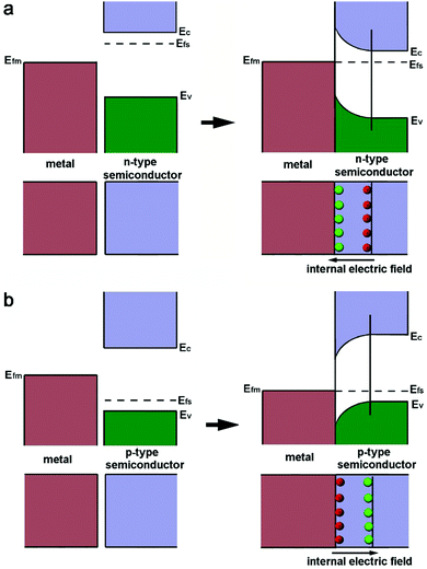 | ||
| Fig. 1 Schematics illustrating the processes of forming the Schottky junction between a metal and (a) an n-type semiconductor or (b) a p-type semiconductor. Reproduced with permission from ref. 12. Copyright 2015 Royal Society of Chemistry. | ||
Given this static interfacial electronic effect, it is anticipated that semiconductor supports may play a role in tailoring the surface charge states of metal catalysts. As a matter of fact, n-type semiconductors have been widely used as supports for metal catalysts in various organic reactions.41–43 Most recently, Zheng et al. developed a stable atomically dispersed Pd–TiO2 catalyst (namely, Pd1/TiO2) in which single Pd atoms are stabilized with ethylene glycolate (EG) on ultrathin TiO2 nanosheets (Fig. 2a and b).44 This catalyst exhibits 9 times higher catalytic activity in hydrogenation of C![[double bond, length as m-dash]](https://www.rsc.org/images/entities/char_e001.gif) C bonds than commercial Pd catalysts in terms of surface Pd atoms (Fig. 2c). It is believed that the static electronic effect plays an important role in the catalytic performance enhancement. As suggested by first-principles simulations (Fig. 2d), the Pd atoms supported on TiO2 can efficiently split the adsorbed H2 into H atoms. While one H atom migrates to the EG nearby, the other H atom would form Pd–Hδ− which can in turn transfer to C
C bonds than commercial Pd catalysts in terms of surface Pd atoms (Fig. 2c). It is believed that the static electronic effect plays an important role in the catalytic performance enhancement. As suggested by first-principles simulations (Fig. 2d), the Pd atoms supported on TiO2 can efficiently split the adsorbed H2 into H atoms. While one H atom migrates to the EG nearby, the other H atom would form Pd–Hδ− which can in turn transfer to C![[double bond, length as m-dash]](https://www.rsc.org/images/entities/char_e001.gif) C for efficient hydrogenation.
C for efficient hydrogenation.
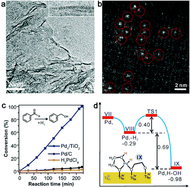 | ||
| Fig. 2 (a) TEM and (b) HAADF-STEM images of a Pd1–TiO2 catalyst. (c) Catalytic performance of Pd1–TiO2 and reference catalysts in styrene hydrogenation. (d) Energies and models of intermediates and transition states in the heterolytic H2 activation process for Pd1–TiO2. Reproduced with permission from ref. 44. Copyright 2016 American Association for the Advancement of Science. | ||
In general, the enhancement of catalytic activities by semiconductor supports is not very significant as the static interfacial electronic effect can only accumulate a limited number of electrons on metal catalysts. To make full use of the Schottky junction for enhanced catalysis, one can employ light illumination to excite the n-type semiconductor and transfer a large number of electrons to metal catalysts as a dynamic interfacial electronic effect. Under light illumination, the electrons in n-type semiconductors are elevated to the conduction band while the holes are left in the valence band. Once the electron–hole pairs enter the space charge region, the photogenerated electrons in the conduction band and the holes in the valence band will migrate to the bulk semiconductor and the metal under the effect of an internal electric field, respectively. Under the successive photoexcitation of the semiconductor, a large number of electrons will be accumulated in the semiconductor, making them energetic enough to transfer to the metal.12 The Schottky barrier will in turn prevent the electron from drifting back to the semiconductor. As such, the electron density of the metal surface can be increased. Similarly, photoexcitation can substantially reduce the electron density of the metal surface when a p-type semiconductor is used as a support.12
Here we employ oxygen activation on a Pd surface as a model reaction to demonstrate the mechanisms. For most oxidation reactions, the activation of molecular oxygen is an important process determining catalytic performance.45–49 The molecular adsorption is a process that highly depends on the atomic arrangement and charge state of the catalyst surface.50–52 In 2013, we found that molecular oxygen can be better activated at the Pd{100} surface than Pd{111}.17 As shown in Fig. 3a and b, the molecular O2 is better activated on Pd{100} according to the larger O–O bond length (1.402 Å on {100} versus 1.324 Å on {111}), which has been verified by synchrotron radiation-based near-edge X-ray absorption fine structure spectroscopy (NEXAFS). During the activation process, an electron transfer takes place from Pd to O2 molecules. The transferred electrons occupy the antibonding orbital of oxygen so as to activate the molecule. In principle, the more electrons are transferred, the better oxygen is activated. The spin charge density analyses (Fig. 3c and d) revealed that about 0.7 electrons can be transferred from the Pd{100} surface to the adsorbed O2, while the charge transfer in the case of Pd{111} was only∼0.4 electron charge. Thus the different amounts of electrons transferred into the anti-bonding π* orbital of O2 should be the fundamental reason for the differentiated O2 activation behavior. For this reason, the catalytic performance of Pd{100} in O2 activation and oxidation reactions can be further enhanced by increasing its electron density. As displayed in Fig. 3e, higher electron density of the Pd surface enables the stretching of O–O bonds, leading to better O2 activation.27
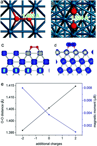 | ||
| Fig. 3 The most favorable adsorption configurations of O2 on (a) Pd{100} facets and (b) Pd{111} facets. The spin charge densities of O2 on (c) Pd{100} facets and (d) Pd{111} facets. Reproduced with permission from ref. 17. Copyright 2013, American Chemical Society. (e) Curves showing the changes in O–O distance and O2 magnetic moment by introducing additional electrons or holes into the Pd{100} system. Reproduced with permission from ref. 27. Copyright 2014 John Wiley. | ||
To increase the electron density of the Pd surface, we developed Pd–TiO2 hybrid structures (Fig. 4a and b) in which TiO2 can be used as the electron donor to modulate the charge state of the Pd surface under light illumination owing to the metal–semiconductor Schottky junction.27 We have employed 2,2,6,6-tetramethyl-4-piperidone hydrochloride (4-oxo-TMP) as a probe molecule to examine the activated oxygen species, which can produce nitroxide radicals (4-oxo-TEMPO) upon trapping the oxygen species. The electron spin resonance (ESR) spectra in Fig. 4c show that the signals for 4-oxo-TEMPO can be enhanced with the Pd–TiO2 hybrid structures compared with bare Pd. This suggests that integrating the Pd{100} catalyst with an n-type semiconductor surely promotes the ability of Pd in activating O2. When implemented for catalytic oxidation of glucose, the Pd–TiO2 catalyst exhibits excellent catalytic activity in glucose oxidation under illumination, especially at the light intensity of 5.6 mW cm−2 (Fig. 4d). Certainly a strong dependence of performance on light intensity has also been observed. The complex charge kinetics in this system has been revealed by our ultrafast absorption spectroscopy characterizations.27 It indicates that too strong light illumination may induce the generation of plasmonic hot electrons on Pd although it is a metal with weak plasmonic properties.53,54 The generated plasmonic hot electrons are injected into the conduction band of TiO2, which lowers the electron density of the Pd surface and reduces the efficacy of the Schottky junction in enhancing O2 activation.12,14,27 Nevertheless, this case well demonstrates that the dynamic interfacial electronic effect by the metal–semiconductor interface under light illumination can provide a powerful approach to tailor the surface charge states of metal catalysts.
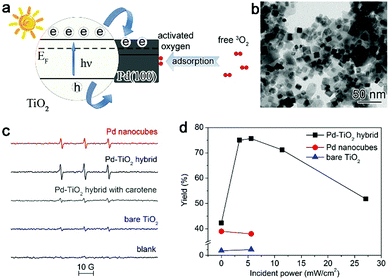 | ||
| Fig. 4 (a) Schematic illustrating the working mechanism for the enhancement of O2 activation using a Pd–TiO2 hybrid structure. (b) TEM image of the Pd–TiO2 hybrid structure. (c) ESR spectra of the samples formed by mixing a solution of 4-oxo-TMP with Pd nanocubes, the Pd–TiO2 hybrid structure and bare TiO2. (d) Catalytic activity of Pd nanocubes, the Pd–TiO2 hybrid structure and bare TiO2 for glucose oxidation under incident UV light with different power intensities. Reproduced with permission from ref. 27. Copyright 2014 John Wiley. | ||
2.2 Interfacing with metals
The electron density of a metal surface can also be tailored by interfacing with another metal material. The mechanism is quite similar to the principle of a galvanic cell (also called voltaic cell) – an electrochemical cell that derives electrical energy from spontaneous redox reactions taking place within the cell. The voltaic pile, invented by Alessandro Volta in the 1800s, consists of a pile of cells with different metals (e.g., Cu and Zn). The potential difference of metals is utilized to induce electron accumulation at the metal side with a high work function, eventually generating electricity in the devices. We call this effect interfacial charge polarization. For instance, the work functions of Pd{100} and Pt{100} are 5.14 and 5.68 eV, respectively. This work function difference causes an electron to transfer from Pd to Pt so as to equilibrate the electron Fermi distribution at their interface. As indicated by the simulated differential charge density (Fig. 5), distinct interfacial polarization occurs when the Pt atoms are of 1–2 atomic layers, resulting in a substantial accumulation of negative charges on the Pt surface. However, as the Pt thickness reaches 4 atomic layers, the surface polarization effect becomes substantially weaker. In other words, the thinner the thickness, the more the charges accumulated on the Pt surface. This increased electron density on the Pt surface would facilitate a number of catalytic applications.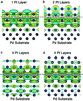 | ||
| Fig. 5 Differential charge density by first-principles simulations illustrating the alterations of electron distributions with the Pt thickness: (a) 1 layer, (b) 2 layers, (c) 3 layers and (d) 4 layers. The olive and cyan colors represent increase and decrease in electron density, respectively. Reproduced with permission from ref. 16. Copyright 2014 John Wiley. | ||
A typical catalytic application facilitated by the interfacial charge polarization is the electrocatalytic hydrogen evolution reaction (HER, 2H+ + 2e− → H2) – a highly important process for hydrogen generation constituting reversible hydrogen fuel cell technology.55–61 Pt is the most efficient electrocatalyst for the HER due to its low overpotential and high current density; however, the usage of Pt is yet to be significantly reduced to minimize material costs. Enabled by the interfacial charge polarization, we have developed an approach to reduce Pt usage and boost HER performance at the same time. As along as the Pt layers on Pd substrates are thin enough, the interfacial charge polarization can accumulate negative charges on the Pt surface to facilitate hydrogen evolution. The developed design is based on a Pt–Pd-reduced graphene oxide (rGO) stack structure with controllable Pt thickness ranging from 0.8 nm to 3.2 nm (Fig. 6a–c).16 As anticipated, the Pt–Pd–rGO I sample with the thinnest Pt shells (0.8 nm) exhibits a current density of 791 mA cm−2 at a potential of −300 mV, dramatically larger than that of the other two samples (Fig. 6d). This suggests that the low thickness of Pt shells is more favorable for HER performance. In addition, the calculated Tafel slope of 10 mV decade−1 for Pt—Pd–rGO I is the lowest among those reported for HER electrocatalysts (Fig. 6e). This further demonstrates that the HER performance has a strong correlation with the Pt thickness, in accordance with the proposed interfacial charge polarization mechanism. Accordingly, the requirement for ultrathin Pt shells by this working mechanism also meets our demand for reducing Pt usage.
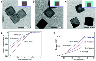 | ||
| Fig. 6 TEM images for (a) Pd–Pt–rGO I with 0.8 nm Pt shell thickness, (b) Pd–Pt–rGO II with 1.8 nm Pt shell thickness and (c) Pd–Pt–rGO III with 3.2 nm Pt shell thickness. (e) Polarization curves and (f) corresponding Tafel plots of Pd–Pt–rGO I, II and III, respectively. Reproduced with permission from ref. 16. Copyright 2014 John Wiley. | ||
Another example sharing a similar working mechanism is the cocatalyst design for photocatalytic water splitting – a promising approach to transform solar energy into hydrogen fuel.62–64 A typical process of photocatalysis involves three steps – light absorption, electron–hole separation, and surface reactions. To improve the efficiencies of the latter two steps, metal cocatalysts are widely used for integration with semiconductor photocatalysts. The cocatalyst not only promotes electron–hole separation via the Schottky junction, but also provides active sites for H2O adsorption and activation, opening the possibility of improving the overall photocatalytic efficiency.12,40,65 There is no doubt that Pt is the most active cocatalyst for hydrogen evolution in water splitting but still suffers from high material cost. To overcome this limitation, the interfacial charge polarization is implemented in the cocatalyst design for this application, similarly to the HER system.
In this case, Pt is deposited on the Pd nanocubes, which are loaded on TiO2 nanosheets to form the TiO2–Pd@Pt quasi-core–shell structure with controllable Pt thickness (Fig. 7a).15 As illustrated in Fig. 7b, this design utilizes the Schottky junction between TiO2 and Pd to trap the photoexcited electrons on Pd, and then induces the electron accumulation at the outer surface of Pt through interfacial charge polarization. As indicated by Table 1, the high electron density on the Pt surface can enhance the adsorption of H2O molecules and thus facilitate the water splitting process.
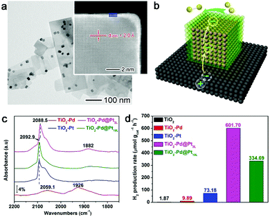 | ||
| Fig. 7 (a) TEM image of a TiO2–Pd@Pt3L sample with the Pt shell thickness of 3 atomic layers. (b) Schematic illustrating the working mechanism for interfacial charge polarization in photocatalytic water splitting. (c) CO chemisorption DRIFTS spectra of TiO2–Pd@Pt3L and TiO2–Pd@Pt10L in reference to TiO2–Pt and TiO2–Pd hybrid structures. (d) Photocatalytic H2 evolution from water with TiO2, TiO2–Pd, TiO2–Pt, TiO2–Pd@Pt3L and TiO2–Pd@Pt10L, respectively. Reproduced with permission from ref. 15. Copyright 2015 John Wiley. | ||
| Structural model | Pd5L@ Pt1L | Pd5L@ Pt2L | Pd5L@ Pt3L | Pd5L@ Pt4L | Pt5L@ Pt4L |
|---|---|---|---|---|---|
| E ad (eV) neutral | −0.346 | −0.252 | −0.263 | 0.664 | −0.101 |
| E ad (eV) with 1e− | −4.317 | −4.627 | −4.892 | −4.495 | −4.161 |
The effect of interfacial charge polarization can make a significant contribution to the electron accumulation on the Pt surface only when the Pt shell thickness is less than 4 atomic layers. The increased electron density has been proven by diffuse reflectance infrared Fourier transform spectroscopy (DRIFTS) using CO as a probe molecule. During the chemisorption, the CO molecules can accept electrons from the Pt surface to enter their antibonding orbitals. At higher electron density, the Pt surface would donate more electrons to the antibonding orbitals of CO molecules, which reduces the vibrational frequency of CO.66Fig. 7c shows that the vibrational frequency for CO chemisorption has been lowered by the TiO2–Pd@Pt3L with 3 atomic Pt layers. This suggests the higher electron density of the Pt surface with respect to TiO2–Pt and TiO2–Pd@Pt10L. The increased electron density can also be confirmed by the reduced binding energies in X-ray photoelectron spectroscopy (XPS).15 As a result, the accumulated electrons on the Pt surface enable a dramatically higher hydrogen production rate by TiO2–Pd@Pt3L (Fig. 7d).
Basically, the interfacial charge polarization is a static electronic effect. Under light illumination, the surface plasmon of noble metal nanostructures will generate plasmonic hot electrons, which may induce a dynamic effect at the metal–metal interfaces. The surface plasmon can be defined as the resonant collective oscillations of the electrons excited by incident photons at the surface of noble metal Au and Ag nanoparticles,19,67 which decays through radiative photon re-emission and non-radiative Landau damping. The non-radiative decay generates energetic electrons and holes, which are commonly referred to as hot electrons and hot holes, respectively. The majority of energetic electrons are dissipated by electron–electron scattering within about 100 femtoseconds. However, a small number of energetic electrons can be transferred to adjacent species, which may alter the catalytic process by maneuvering surface charge densities.
For instance, Pd is a widely used catalyst for organic hydrogenation reactions – a large group of addition reactions of hydrogen at unsaturated bonds, which are among the simplest transformations in organic chemistry and are extensively involved in various chemical processes.68–74 The hydrogenation reactions usually take place through the dissociation of molecular H2 and desorption of Had atoms from the surface.69 As molecular H2 can be easily dissociated at the Pd surface,75 the desorption of Had atoms from the Pd surface becomes the rate-limiting step in the process of hydrogenation reactions. Our simulation (Table 2) indicates that the binding of dissociated H atoms to the Pd surface is enhanced by the addition of one electron, regardless of the locations of H atoms on Pd nanocrystals.20 Thus the high electron densities on the Pd surface (e.g., through plasmonic hot-electron injection) would disfavor hydrogenation reactions.
| Structural model | {100} | {730} | Pd13-a | Pd13-b |
|---|---|---|---|---|
| E ad (eV) neutral | −2.090 | −2.095 | −2.929 | −2.864 |
| E ad (eV) with 1e− | −2.735 | −2.739 | −2.957 | −2.877 |
One of our recent works proved this hypothesis, in which ultrathin layers of catalytic metal Pd are grown on plasmonic gold nanorods (Fig. 8a and b).76 The Pd thickness can be controlled from 2 atomic layers to tens of atomic layers. Once the plasmonic hot electrons are generated in Au, they have to travel through the Pd layers before reaching the reaction species (Fig. 8c). As such, the lifetime of hot electrons can be modulated through Pd layer thickness. We have acquired the time constant of hot electrons using ultrafast absorption spectroscopy, which can be well correlated with catalytic performance (Fig. 8d). The longer the lifetime the plasmonic hot electrons exhibit, the lower the conversion yield the catalytic reaction achieves. This suggests that plasmonic hot electrons indeed make a negative contribution to hydrogenation reactions.
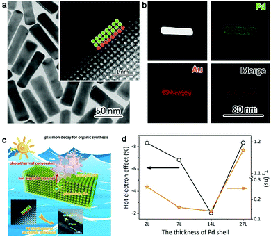 | ||
| Fig. 8 (a) TEM images and (b) EDS mapping profiles of Au–Pd2L core–shell nanostructures with 2 atomic Pd layers. (c) Schematic illustrating the plasmonic effects on styrene hydrogenation by Au–Pd2L core–shell nanostructures. (d) Plasmonic hot-electron effect on styrene hydrogenation under irradiation of λ > 700 nm in comparison with time constants responsible for charge recombination. Reproduced with permission from ref. 76. Copyright 2016 American Chemical Society. | ||
The correlation of hot electron lifetime with the Pd thickness (Fig. 8d) reveals that the plasmonic hot electrons tend to interact more thoroughly with the Pd lattice by increasing Pd shell thickness. This interaction will reduce the number of hot electrons reaching the Pd surface. Nevertheless, if the Pd shells are too thick, hot electrons would be generated by the Pd shells on their own, which brings more electrons to the Pd surface. Thus the charge densities of the Pd surface can be tailored by controlling the Pd thickness over plasmonic nanostructures. Although plasmonic hot electrons suppress the hydrogenation reactions, this working mechanism should be implemented to promote the reactions that require high surface electron densities (e.g., oxygen activation and oxidation reactions). It is anticipated that future works will validate this assumption.
2.3 Interfacing with organic ligands
Organic ligands are key components in homogeneous catalysis which can induce significant steric and electronic effects for catalytically active metal sites to tune catalytic selectivity.77–79 In terms of heterogeneous catalysis, the organic ligands are mainly employed as the agents for improving catalytic selectivity through steric effects or the stabilizers for loading atomically dispersed metal atoms.80–82 In principle, the organic ligands should be capable of creating electronic effects on catalytic sites when the catalytic materials are shrunk to the atomic level. In recent years, it has been demonstrated that such electronic effects can indeed tune catalytic activities.83,84Most recently, Zheng et al. reported that electronic effects can serve as a knob for tuning the selectivity of catalytic reactions in the partial hydrogenation of nitroaromatics to N-hydroxylaniline derivatives (an important class of intermediates for many high-value products85–87).88 The demonstration is based on the ethylenediamine (EDA)-chelated ultrathin Pt nanowires. The nanowires have an ultralow diameter of 1.1 nm (Fig. 9a), which allows the significant electronic effects of EDA on Pt nanowires. As indicated by Bader charge analysis (Fig. 9b), the EDA ligands can donate electrons to Pt nanowires and make the Pt surface highly electron rich. Such an increase in the electron density on the Pt surface favors the adsorption of electron-deficient reactants (i.e., nitroaromatics) and the desorption of electron-rich substrates (i.e., N-hydroxylaniline derivatives) (see Fig. 9c). As a result, full hydrogenation can be effectively prevented to achieve high selectivity in the production of N-hydroxylanilines by EDA-chelated Pt nanowires. As a matter of fact, the electronic effects by EDA ligands can be readily implemented in various Pt catalysts. For instance, when commercial Pt black is treated with Pt(EDA)2(acac)2, the Pt-EDA chelating units can be deposited on the surface. As a result, the EDA-modified Pt black catalyst exhibits a dramatically enhanced selectivity to N-hydroxylaniline derivatives (Fig. 9d and e), which are applicable to nitroaromatics with various substitutions.
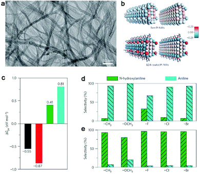 | ||
| Fig. 9 (a) TEM image of EDA-chelated ultrathin Pt nanowires. (b) Structural models and Bader charge analysis for bare Pt nanowires and EDA-chelated Pt nanowires. (c) Free energies (ΔGpo) for the adsorption of N-containing aromatics over EDA-chelated Pt nanowires. Black, nitrobenzene; red, nitrosobenzene; green, N-hydroxylaniline; blue, aniline. Catalytic performance comparison for the hydrogenation of substituted nitrobenzene over Pt black (d) before and (e) after Pt(EDA)2(acac)2 modification. Reproduced with permission from ref. 88. Copyright 2016 Nature Publishing Group. | ||
As the electronic effects of organic ligands have been extensively investigated in homogeneous catalysis – the main branch in organic chemistry studied for centuries – we would envision that many concepts and findings can be borrowed from traditional organic chemistry in the future. Moreover, despite rare attempts in dynamic electronic effects, it is anticipated that some photosensitizers can be employed as ligands to integrate with heterogeneous catalysts for light-enhanced catalysis.
3. Engineering the surface charge states of semiconductor catalysts
In addition to noble metals, metal oxides and chalcogenides are a class of catalysts at lower material costs. For instance, metal oxides have been widely employed as catalysts for CO oxidation – a typical reaction well studied in heterogeneous catalysis.18,32,33,89–91 Many metal oxides and chalcogenides possess semiconductor characteristics, which provides an opportunity for tuning their catalytic performance through electronic effects.3.1 Creating defects in ultrathin two-dimensional nanostructures
As the surface charge density of catalysts plays a key role in catalysis, ultrathin two-dimensional nanosheets that offer high charge density provide an opportunity for achieving high catalytic performance. Taking CO oxidation as an example, the high charge density can promote the activation of oxygen and accelerate CO diffusion, facilitating the CO oxidation process.The high catalytic performance of ultrathin two-dimensional nanosheets is related to their large surface area, abundant active sites and high carrier concentration. For instance, SnO2 nanosheets with 5 atomic layers at the thickness of about 0.66 nm can be obtained by EDA-assisted synthesis.32 The unique electronic structures of the 0.66 nm SnO2 nanosheets enable their excellent activities in CO oxidation, with lower conversion temperature and lower activation energy, as compared with 1.9 nm SnO2 nanosheets, SnO2 nanoparticles and bulk SnO2 (Fig. 10a and b). As metal oxides such as SnO2 serve as catalysts, CO oxidation generally follows the Mars van Krevelen mechanism.92 In this case, CO diffusion is one of the important factors that affect the catalytic activities. The density of states (DOS) and charge density contour plots show the increased charge density at the valence band of ultrathin SnO2 nanosheets (Fig. 10c–f). This feature would result in fast electron transport to facilitate CO diffusion so that CO can more efficiently react with the activated O atom, improving the overall performance of CO oxidation.
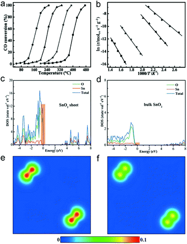 | ||
| Fig. 10 (a) Catalytic activity for CO oxidation vs. reaction temperature for 0.66 nm SnO2 nanosheets, 1.9 nm SnO2 nanosheets, SnO2 nanoparticles and bulk SnO2 (from left to right). (b) The corresponding Arrhenius plots. Calculated density of state (DOS) for (c) 0.66 nm SnO2 nanosheets and (d) bulk SnO2. Charge density contour plots projected along the (100) plane for the valance band maximum of (e) 0.66 nm SnO2 nanosheets and (f) bulk SnO2. Reproduced with permission from ref. 32. Copyright 2013 John Wiley. | ||
The atomically thin nanosheets set up a platform for further engineering the subtle features toward tunable charge densities. The surface defect is such a structural feature in ultrathin nanosheets that can further boost CO oxidation activity. Taking ultrathin CeO2 nanosheets with surface pits as an example, two different kinds of coordinated Ce atoms are generated on account of plentiful surface pits: the 4-coordinated Ce atom at which CO is more likely to adsorb, and the 5-coordinated Ce atom at which O2 prefers to adsorb and activate (Fig. 11a).33 During the formation of CO2, CO should overcome a diffusion barrier to react with the adjacent O atom. The pit-surrounding Ce sites help to increase the hole carrier density by increasing the DOS near the Fermi level (Fig. 11b), thereby lowering the CO diffusion barrier. In this case, the CO adsorbed at the 4-coordinated Ce site can easily diffuse to the O atom absorbed at the neighboring 5-coordinated Ce site to produce CO2. Although O2 activation is the rate-determining step in CO oxidation, the reduced CO diffusion barrier caused by the increased carrier density also contributes to lowering the overall activation energy. As a result, the ultrathin CeO2 nanosheets with surface pits can efficiently improve the CO oxidation rate and lower the activation energy (Fig. 11c and d). It is anticipated that lattice engineering on ultrathin two-dimensional nanostructures with semiconductor characteristics can create more efficient catalysts for other catalytic applications from the angle of electronic effects.
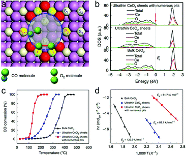 | ||
| Fig. 11 (a) Top-view structural schematic for CeO2 nanosheets with 3 atomic layers and with numerous pits on the surface. CO molecules prefer to adsorb at the P2 site, while O2 molecules tend to adsorb and dissociate at the adjacent P1 sites. (b) Calculated densities of states (DOS) for the ultrathin CeO2 nanosheets with numerous pits, ultrathin CeO2 nanosheets and bulk CeO2. (c) Catalytic activities for CO oxidation vs. reaction temperature and (d) the corresponding Arrhenius plots for the three catalysts. Reproduced with permission from ref. 33. Copyright 2013 Nature publishing Group. | ||
However, it is worth mentioning that the defects are often the centers for charge recombination particularly in the case of light illumination (i.e., dynamic charge systems).12,93–97 As ultrathin two-dimensional nanostructures are further interfaced with other materials (e.g., metals), charge recombination would become more severe at the defects existing at the interfaces (i.e., interfacial defects).13,93–97 Thus creating defects toward tunable charge states requires systematic study in which the material models and their interlinked effects should be carefully analyzed.
3.2 Interfacing with metals
Similarly to the case of metal catalysts, the surface charge states of semiconductor catalysts can also be tailored through interfacial electronic effects. Here we first name an example using CO oxidation as a model reaction. Cu2O/CuO is a catalyst that has been intensively investigated for CO oxidation owing to its relatively high catalytic activity.89 Recently we have revealed that interfacial charge polarization can enhance the catalytic activity of Cu2O/CuO through integration with Ag.18 In the synthesis, Cu2O is grown on Ag nanoplates in the solution phase, in which the coverage of Cu2O on Ag can be well controlled to form tunable interfacial lengths. As a result, three Ag–Cu2O samples with various partial coverage and full coverage sample can be obtained, while Cu2O frames are prepared by removing Ag as a reference sample (Fig. 12a–e). Prior to the catalytic assessment, all the samples have been treated in a cycle of CO oxidation to form a stable CuO surface. Our catalytic assessment (Table 3) indicates that the apparent activation energies can be dramatically reduced to 36.7–42.7 kJ mol−1 with partial coverage, which should be ascribed to the exposed Ag–CuO interfaces. Moreover, the CO conversion rates turn out to be dependent on the interfacial lengths (Fig. 12f), suggesting that the interfacial lines are the locations of active sites.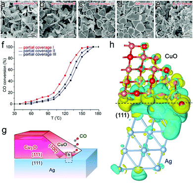 | ||
| Fig. 12 SEM images of (a) partial coverage I, (b) partial coverage II, (c) partial coverage III and (d) full coverage Ag–Cu2O hybrid structures, and (e) Cu2O frames. (f) Catalytic performance of Ag–CuO/Cu2O partial coverage I, II and III samples in Cycle 2 of CO oxidation. (g) Schematic illustration for Ag–CuO/Cu2O hybrid structures with interfacial charge polarization for CO oxidation (side view for the cross-section). (h) Differential charge density by first-principles simulations illustrating the increase (olive color) and decrease (cyan color) of electron distributions in the atomic model for the Ag(111) substrate interfacing with the extension part of the side CuO layer. Reproduced with permission from ref. 18. Copyright 2014 American Chemical Society. | ||
| Sample | Partial cover. I | Partial cover. II | Partial cover. III | Full cover. | Frames |
|---|---|---|---|---|---|
| E a (kJ mol−1) | 42.7 ± 1.5 | 37.0 ± 1.8 | 36.7 ± 1.3 | 62.8 ± 2.1 | 66.4 ± 7.1 |
The high catalytic activity enabled by the exposed Ag–CuO interfaces has been well elucidated by our first-principles simulations. Ag and CuO possess different work functions (4.45 eV vs. 5.97 eV) to induce an interfacial charge polarization effect (Fig. 12g and h), which increases the electron density of the CuO surface near the Ag–CuO interface and dramatically decays with the distance to the interface. Consequently, the increased electron density on the CuO surface can lower the transition energy barrier from 0.60 to 0.24 eV in CO activation as indicated by our simulations. This feature designates the exposed Ag–CuO interface as the location of active sites so that the number of active sites can be readily tailored by controlling the interfacial lengths.
The interfacial charge polarization is also applicable to other materials and reaction systems. For example, MoS2 is a material with a layered structure to replace expensive Pt for electrocatalytic HER application.98–101 As compared with metallic 1T-MoS2, semiconducting 2H-MoS2 is more chemically stable but exhibits relatively low HER activity. The limitation of the 2H-MoS2 catalyst originates from the limited number of active sites – the unsaturated sulfur atoms located along the edges of the MoS2 layers and the low mobility for charge transport.98,100 To overcome this limitation, we have developed a hybrid structure of 2H-MoS2 and Pd nanowires (Fig. 13a).102 As a result, the hybrid structure exhibits a current density of 122 mA cm−2 at −300 mV versus RHE and a Tafel slope of 44 mV decade−1 with excellent durability (Fig. 13b and c), which well exceeds the performance of bare 2H-MoS2 and 1T-MoS2.
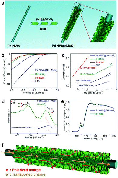 | ||
| Fig. 13 (a) Schematic illustration for the synthesis of a Pd NWs@2H-MoS2 hybrid structure. (b) Polarization curves and (c) the corresponding Tafel plots for the Pd NWs@2H-MoS2 hybrid structure in reference to bare 2H-MoS2, Pd NWs and Pt/C. (d) Raman spectra and (d) S L2,3-edge NEXAFS spectra of the Pd NWs@2H-MoS2 hybrid structure and bare 2H-MoS2. (f) Schematic illustrating the working mechanisms involved in the Pd NWs@2H-MoS2 HER electrocatalyst. Reproduced with permission from ref. 97. Copyright 2016 Springer. | ||
In addition to the improved charge transport by Pd nanowires, the interfacial charge polarization between 2H-MoS2 and Pd is believed to play a key role in the performance enhancement. The difference in their work functions (5.12 eV for Pd vs. 6.53 eV for MoS2) induces the accumulation of negative charges on MoS2 through charge polarization at the Pd–MoS2 interface. XPS characterization indicates that the increased negative charges are donated to the S sites of 2H-MoS2. This argument has been further supported by Raman spectroscopy and NEXAFS spectroscopy. The increased electron density stiffens the out-of-plane vibration of the S atom, which has been resolved by the blue-shifted Raman peak (Fig. 13d). Moreover, the partial occupancy of upper energy levels in S by the donated electrons reduces the probability of the transitions of S 2p electrons to the S s-like state (peak A) and to the empty S 3d state (peak B), which is reflected in the reduced NEXAFS peak intensities (Fig. 13e). As such, the polarized electrons on the S sites can promote the Heyrovsky step – a key step in the HER – enhancing the HER performance. Overall, interfacial electronic effects can serve as a versatile tool for tailoring the electron densities of active sites and maneuvering the catalytic activities in various reaction systems.
4. Summary and outlook
The regulation of surface charge states for catalytic nanostructures exerts an important and far-reaching influence on various catalytic reaction systems. In this article, we summarize the efforts made by our research group and other researchers to tailor the compositions and structures of catalysts through lattice and interface engineering. Interfacial electronic effects have been proven as a powerful tool for tailoring the surface charge states of catalytic materials. Beyond the cases that have been discussed in this article, there would be a number of directions worth exploring in this research field.(1) We mainly focus on the interfaces between metals and/or semiconductors in this review; however, the interfacial electronic effects can generally work for various material types. For instance, the integration of metal catalysts with a ferroelectric substrate also provides an opportunity for tuning catalytic performance with electronic effects.103 The catalytic activity of Ni in ethylene hydrogenation can be maneuvered by altering the substrates (Fig. 14).44
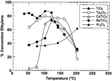 | ||
| Fig. 14 Conversion of ethylene hydrogenation catalyzed by Ni supported on TiO2, Ta2O3, CaTiO3, BaTiO3 and Al2O3, respectively. Reproduced with permission from ref. 103. Copyright 2000 American Chemical Society. | ||
When supported on γ-Al2O3, the conversion yield is raised along with the increase of temperature. Nevertheless, as the Ni supported on ferroelectric materials catalyzes the hydrogenation of ethylene, the reaction exhibits parabola-like rules around the substrate’s Curie temperature (e.g., the Curie temperature of BaTiO3 is 120–130 °C). It is well known that the chemical structures and charge densities of ferroelectric materials will dramatically change at the Curie temperature owing to internal electronic polarization. As a consequence, the polarization of ferroelectric materials promotes electronic perturbation especially at the Curie temperature. This promotion in turn changes the chemical structure and charge density of the metal catalyst, and hence influences the catalytic activity. This case highlights that future efforts should be made for substrate engineering toward catalytic performance tuning. As a matter of fact, substrate engineering has been widely investigated in organic synthesis; however, more attention should be paid to electronic effects in future studies.
(2) The utilization of interfacial electronic effects with organic ligands is another direction in this field, which has been briefly discussed in Section 2.3. Organic ligands have been widely used in homogeneous catalysis, so many concepts of traditional organic chemistry can be borrowed to maneuver the surface charge states of heterogeneous catalysts. Furthermore, this strategy should be able to extend to other soft matters such as polymers with coordination atoms. Our recent work indicates that polymeric materials can play a similar role to organic ligands in tuning electronic structures.104
(3) In addition to the material design alone, external field is another possible approach to tune catalytic performance through electronic effects. In solid-state electrochemistry, the activity and selectivity of metal catalysts can be modified by the non-Faradaic electrochemical modification of catalytic activity (NEMCA) effect.7 However, only when the interface of the metal and solid–electrolyte is fully polarized can the NEMCA effect happen. Fig. 15a shows the principle of NEMCA in a solid–electrolyte cell composed of gaseous reactants, metal catalyst |ZrO2–Y2O3|M and O2. The concentration of O2− at the polarized metal–electrolyte interface can be changed by applying an external voltage, which induces a variation in work function and thus adjusts the catalytic reaction rate. As the polarization-induced NEMCA effect is used in Pt-catalyzed ethylene oxidation reaction, the catalytic reaction rate and activation energy exhibit exponential and linear relationships with the work function, respectively (Fig. 15b). Consequently, the polarization can serve as an effective electron regulatory tool for varying the ion concentration and work function, further optimizing the catalytic properties. Thus the use of an external magnetic or electric field would become a promising strategy for tuning catalytic performance complementarily to material design.
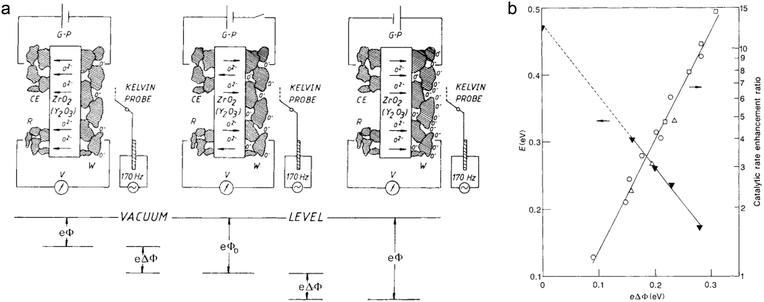 | ||
| Fig. 15 (a) Principle of NEMCA. The right (left) side of panel a shows the supply (removal) of oxide anions (O2−) to (from) the polarized solid-electrolyte/catalyst (W) interface. The electrochemically induced spillover of oxygen anions O− produced (consumed) at the solid-electrolyte/catalyst/gas three-phase boundaries causes an increase (decrease) in the catalyst work function (eΔΦ). (b) Impact of catalyst work function on the activation energy (E) and catalytic rate enhancement ratio (r/ro) for C2H4 oxidation on Pt. Reproduced with permission from ref. 7. Copyright 1990 Nature Publishing Group. | ||
(4) As discussed in Sections 2.1 and 2.2, light illumination on reaction systems would induce dynamic interfacial electronic effects, which opens up the possibility of harvesting solar energy to drive catalytic reactions. The dynamic process is rather complex but offers a broader range for modulating surface charge states as compared with static electronic effects. This research would be performed at the intersection with photocatalysis and plasmonics.12 In this case, charge separation is a key process for the enhancement of catalytic performance.12
Plenty of opportunities are usually accompanied with grand challenges. In spite of the considerable progress, research into novel hybrid catalytic systems designed to regulate surface charge states still has a long way to go. The challenges mainly come from two aspects. (1) This research calls for future efforts on lattice and interface engineering at atomic precision for catalyst design, in efforts to rationally control surface charge states. Large-scale production techniques for catalysts have to be developed before moving forward to the next application stage. (2) The fundamental understanding in this research field has yet to be deepened, and more information should be collected to bridge the catalyst structures, surface charge states and catalytic performance. In this case, we have to develop characterization techniques for surface and interface structures at atomic resolution, surface charge states at high spatial resolution, dynamic charge transfer processes at high temporal resolution, and in situ chemical reactions. Synchrotron radiation-based spectroscopy and ultrafast spectroscopy are the currently used techniques with relatively high spatial and temporal resolutions. In particular, it is imperative to develop operando surface characterization techniques for directly probing the surface charge states. For instance, Salmeron et al. has employed ambient-pressure XPS (APXPS) to measure the charge state of Au nanoparticles supported on TiO2 under O2 pressure, which provides valuable information for decoding the mechanism for high catalytic activities in various reactions such as CO oxidation.105
Overall, it is anticipated that further research on the catalyst design from the angle of surface charge states will definitely strengthen our capability of controlling catalytic activity and selectivity. Moreover, the modification on surface charge states will provide a new train of thought for industrial production of advanced materials to realize the efficient utilization of energy and the maximization of atom economy. Apart from the surface charge states, other factors such as reaction dynamics may make contributions to the enhanced catalytic performance. Taken together, the factors tightly controlled in a well-designed system would boost the overall catalytic performance.
Acknowledgements
This work was financially supported in part by NSFC (no. 21471141, U1532135, 21601173, 21573212), CAS Key Research Program of Frontier Sciences (QYZDB-SSW-SLH018), Recruitment Program of Global Experts, CAS Hundred Talent Program, and Anhui Provincial Natural Science Foundation (1608085QB24, 1508085MB24).Notes and references
- J. K. Nørskov, T. Bligaard, J. Rossmeisl and C. H. Christensen, Nat. Chem., 2009, 1, 37 CrossRef PubMed.
- J. A. Schwarz, C. Contescu and A. Contescu, Chem. Rev., 1995, 95, 477 CrossRef CAS.
- Y. N. Xia, Y. J. Xiong, B. Lim and S. E. Skrabalak, Angew. Chem., Int. Ed., 2009, 48, 60 CrossRef CAS PubMed.
- T. Fujita, P. F. Guan, K. McKenna, X. Y. Lang, A. Hirata, L. Zhang, T. Tokunaga, S. Arai, Y. Yamamoto, N. Tanaka, Y. Ishikawa, N. Asao, Y. Yamamoto, J. Erlebacher and M. W. Chen, Nat. Mater., 2012, 11, 775 CrossRef CAS PubMed.
- H. Zhang, M. S. Jin, Y. J. Xiong, B. Lim and Y. N. Xia, Acc. Chem. Res., 2013, 46, 1783 CrossRef CAS PubMed.
- G. Liu, H. G. Yang, J. Pan, Y. Q. Yang, G. Q. Lu and H. M. Cheng, Chem. Rev., 2014, 114, 9559 CrossRef CAS PubMed.
- C. G. Vayenas, S. Bebelis and S. Ladas, Nature, 1990, 343, 625 CrossRef CAS.
- L. E. Brus, J. Chem. Phys., 1984, 80, 4403 CrossRef CAS.
- R. Rossetti, J. L. Ellison, J. M. Gibson and L. E. Brus, J. Chem. Phys., 1984, 80, 4464 CrossRef CAS.
- Y. F. Sun, S. Gao and Y. Xie, Chem. Soc. Rev., 2014, 43, 530 RSC.
- Z. C. Zhang, B. Xu and X. Wang, Chem. Soc. Rev., 2014, 43, 7870 RSC.
- S. Bai, J. Jiang, Q. Zhang and Y. J. Xiong, Chem. Soc. Rev., 2015, 44, 2893 RSC.
- L. L. Wang, J. Ge, A. L. Wang, M. S. Deng, X. J. Wang, S. Bai, R. Li, J. Jiang, Q. Zhang, Y. Luo and Y. J. Xiong, Angew. Chem., Int. Ed., 2014, 53, 5107 CAS.
- S. Bai, X. Y. Li, Q. Kong, R. Long, C. M. Wang, J. Jiang and Y. J. Xiong, Adv. Mater., 2015, 27, 3444 CrossRef CAS PubMed.
- S. Bai, L. Yang, C. L. Wang, Y. Lin, J. L. Lu, J. Jiang and Y. J. Xiong, Angew. Chem., Int. Ed., 2015, 54, 14810 CrossRef CAS PubMed.
- S. Bai, C. M. Wang, M. S. Deng, M. Gong, Y. Bai, J. Jiang and Y. J. Xiong, Angew. Chem., Int. Ed., 2014, 53, 12120 CrossRef CAS PubMed.
- R. Long, K. K. Mao, X. D. Ye, W. S. Yan, Y. B. Huang, J. Y. Wang, Y. Fu, X. S. Wang, X. J. Wu, Y. Xie and Y. J. Xiong, J. Am. Chem. Soc., 2013, 135, 3200 CrossRef CAS PubMed.
- Y. Bai, W. H. Zhang, Z. H. Zhang, J. Zhou, X. J. Wang, C. M. Wang, W. X. Huang, J. Jiang and Y. J. Xiong, J. Am. Chem. Soc., 2014, 136, 14650 CrossRef CAS PubMed.
- P. Christopher, H. L. Xin and S. Linic, Nat. Chem., 2011, 3, 467 CAS.
- R. Long, Z. L. Rao, K. K. Mao, Y. Li, C. Zhang, Q. L. Liu, C. M. Wang, Z. Y. Li, X. J. Wu and Y. J. Xiong, Angew. Chem., Int. Ed., 2015, 54, 2425 CrossRef CAS PubMed.
- Y. Bai, R. Long, C. M. Wang, M. Gong, Y. R. Li, H. Huang, H. Xu, Z. Q. Li, M. S. Deng and Y. J. Xiong, J. Mater. Chem. A, 2013, 1, 4228 CAS.
- L. Ma, C. M. Wang, B. Y. Xia, K. K. Mao, J. W. He, X. W. Wu, Y. J. Xiong and X. W. Lou, Angew. Chem., Int. Ed., 2015, 54, 5666 CrossRef CAS PubMed.
- R. Bashyam and P. Zelenay, Nature, 2006, 443, 63 CrossRef CAS PubMed.
- J. Shi, Chem. Rev., 2013, 113, 2139 CrossRef CAS PubMed.
- A. Dedieu, Chem. Rev., 2000, 100, 543 CrossRef CAS PubMed.
- A. Furstner and P. W. Davies, Angew. Chem., Int. Ed., 2007, 46, 3410 CrossRef PubMed.
- R. Long, K. K. Mao, M. Gong, S. Zhou, J. H. Hu, M. Zhi, Y. You, S. Bai, J. Jiang, Q. Zhang, X. J. Wu and Y. J. Xiong, Angew. Chem., Int. Ed., 2014, 53, 3205 CrossRef CAS PubMed.
- S. M. Kim, S. J. Lee, S. H. Kim, S. Kwon, K. J. Yee, H. Song, G. A. Somorjai and J. Y. Park, Nano Lett., 2013, 13, 1352 CrossRef CAS PubMed.
- J. Y. Park, L. R. Baker and G. A. Somorjai, Chem. Rev., 2015, 115, 2781 CrossRef CAS PubMed.
- J. Y. Park, S. M. Kim, H. Lee and I. I. Nedrygailov, Acc. Chem. Res., 2015, 48, 2475 CrossRef CAS PubMed.
- H. J. Freund, G. Meijer, M. Scheffler, R. Schlögl and M. Wolf, Angew. Chem., Int. Ed., 2011, 50, 10064 CrossRef CAS PubMed.
- Y. F. Sun, F. C. Lei, S. Gao, B. C. Pan, J. F. Zhou and Y. Xie, Angew. Chem., Int. Ed., 2013, 52, 10569 CrossRef CAS PubMed.
- Y. F. Sun, Q. H. Liu, S. Gao, H. Cheng, F. C. Lei, Z. H. Sun, Y. Jiang, H. B. Su, S. Q. Wei and Y. Xie, Nat. Commun., 2013, 4, 2899 Search PubMed.
- J. Repp, G. Meyer, F. E. Olsson and M. Persson, Science, 2004, 305, 493 CrossRef CAS PubMed.
- L. Giordano and G. Pacchioni, Acc. Chem. Res., 2011, 44, 1244 CrossRef CAS PubMed.
- Y. Cui, C. Stiehler, N. Nilius and H.-J. Freund, Phys. Rev. B: Condens. Matter Mater. Phys., 2015, 92, 075444 CrossRef.
- G. Pacchioni, L. Giordano and M. Baistrocchi, Phys. Rev. Lett., 2005, 94, 226104 CrossRef PubMed.
- N. Cabrera and N. F. Mott, Rep. Prog. Phys., 1948, 12, 163 Search PubMed.
- S. M. Sze, Semiconductor Devices: Physics and Technology, Wiley, 2nd edn, 2001 Search PubMed.
- A. L. Linsebigler, G. Lu and J. T. Yates Jr., Chem. Rev., 1995, 95, 735 CrossRef CAS.
- L. Kesavan, R. Tiruvalam, M. H. A. Rahim, M. I. B. Saiman, D. I. Enache, R. L. Jenkins, N. Dimitratos, J. A. Lopez-Sanchez, S. H. Taylor, D. W. Knight, C. J. Kiely and G. J. Hutchings, Science, 2011, 331, 195 CrossRef CAS PubMed.
- D. I. Enache, J. K. Edwards, P. Landon, B. Solsona-Espriu, A. F. Carley, A. A. Herzing, M. Watanabe, C. J. Kiely, D. W. Knight and G. J. Hutchings, Science, 2006, 311, 362 CrossRef CAS PubMed.
- T. Ishida, N. Kinoshita, H. Okatsu, T. Akita, T. Takei and M. Haruta, Angew. Chem., Int. Ed., 2008, 47, 9265 CrossRef CAS PubMed.
- P. Liu, Y. Zhao, R. Qin, S. Mo, G. Chen, L. Gu, D. M. Chevrier, P. Zhang, Q. Guo, D. Zang, B. Wu, G. Fu and N. Zheng, Science, 2016, 352, 797 CrossRef CAS PubMed.
- K. Chung, S. M. Banik, A. G. De Crisci, D. M. Pearson, T. R. Blake, J. V. Olsson, A. J. Ingram, R. N. Zare and R. M. Waymouth, J. Am. Chem. Soc., 2013, 135, 7593 CrossRef CAS PubMed.
- D. I. Enache, J. K. Edwards, P. Landon, B. Solsona-Espriu, A. F. Carley, A. A. Herzing, M. Watanabe, C. J. Kiely, D. W. Knight and G. J. Hutchings, Science, 2006, 311, 362 CrossRef CAS PubMed.
- K. Mori, T. Hara, T. Mizugaki, K. Ebitani and K. Kaneda, J. Am. Chem. Soc., 2004, 126, 10657 CrossRef CAS PubMed.
- M. Besson, F. Lahmer, P. Gallezot, P. Fuertes and G. Fleche, J. Catal., 1995, 152, 116 CrossRef CAS.
- G. Collins, M. Schmidt, C. O. Dwyer, J. D. Holmes and G. P. McGlacken, Angew. Chem., Int. Ed., 2014, 53, 4142 CrossRef CAS PubMed.
- X. Xie, Y. Li, Z.-Q. Liu, M. Haruta and W. Shen, Nature, 2009, 458, 746 CrossRef CAS PubMed.
- A. Hellman, S. Klacar and H. Gronbeck, J. Am. Chem. Soc., 2009, 131, 16636 CrossRef CAS PubMed.
- C. Li, T. Sato and Y. Yamauchi, Chem. Commun., 2014, 50, 11753 RSC.
- G. V. Hartland, Chem. Rev., 2011, 111, 3858 CrossRef CAS PubMed.
- Y. Xiong, J. Chen, B. Wiley, Y. Xia, Y. Yin and Z. Y. Li, Nano Lett., 2005, 5, 1237 CrossRef CAS PubMed.
- C. G. Morales-Guio, L. A. Stern and X. Hu, Chem. Soc. Rev., 2014, 43, 6555 RSC.
- W. F. Chen, J. T. Muckerman and E. Fujita, Chem. Commun., 2013, 49, 8896 RSC.
- H. I. Karuadasa, E. Montalvo, Y. Sun, M. Majda, J. R. Long and C. J. Chang, Science, 2012, 335, 698 CrossRef PubMed.
- L. Cheng, W. Huang, Q. Gong, C. Liu, Z. Liu, Y. Li and H. Dai, Angew. Chem., Int. Ed., 2014, 53, 7860 CrossRef CAS PubMed.
- X. Huang, Z. Zeng, S. Bao, M. Wang, X. Qi, Z. Fan and H. Zhang, Nat. Commun., 2013, 4, 1444 CrossRef PubMed.
- D. V. Psposito, S. T. Hunt, A. L. Stottlemyer, K. D. Dobson, B. E. McCandless, R. W. Birkmire and J. G. Chen, Angew. Chem., Int. Ed., 2010, 49, 9859 CrossRef PubMed.
- N. M. Marković, B. N. Grgur and P. N. Ross, J. Phys. Chem. B, 1997, 101, 5405 CrossRef.
- A. Fujishima and K. Honda, Nature, 1972, 238, 37 CrossRef CAS PubMed.
- R. Asahi, T. Morikawa, T. Ohwaki, K. Aoki and Y. Taga, Science, 2001, 293, 269 CrossRef CAS PubMed.
- K. Maeda, K. Teramura, D. L. Lu, T. Takata, N. Saito, Y. Inoue and K. Domen, Nature, 2006, 440, 295 CrossRef CAS PubMed.
- J. Yang, D. Wang, H. Han and C. Li, Acc. Chem. Res., 2013, 46, 1900 CrossRef CAS PubMed.
- F. A. Cotton, G. Wilkinson, C. A. Murillo and M. Bochmann, Advanced Inorganic Chemistry, Wiley, 6th edn, 1999 Search PubMed.
- S. Linic, P. Christopher and D. B. Ingram, Nat. Mater., 2011, 10, 911 CrossRef CAS PubMed.
- A. M. Smith and R. Whyman, Chem. Rev., 2014, 114, 5477 CrossRef CAS PubMed.
- G. Kyriakou, M. B. Boucher, A. D. Jewell, E. A. Lewis, T. J. Lawton, A. E. Baber, H. L. Tierney, M. Flytzani-Stephanopoulos and E. C. H. Sykes, Science, 2012, 335, 1209 CrossRef CAS PubMed.
- S. Kidambi, J. Dai, J. Li and M. L. Bruening, J. Am. Chem. Soc., 2004, 126, 2658 CrossRef CAS PubMed.
- O. M. Wilson, M. R. Knecht, J. C. Garcia-Martinez and R. M. Crooks, J. Am. Chem. Soc., 2006, 128, 4510 CrossRef CAS PubMed.
- Y. Wang, J. Yao, H. Li, D. Su and M. Antonietti, J. Am. Chem. Soc., 2011, 133, 2362 CrossRef CAS PubMed.
- Y. M. A. Yamada, Y. Yuyama, T. Sato, S. Fujikawa and Y. Uozumi, Angew. Chem., Int. Ed., 2013, 53, 127 CrossRef PubMed.
- T. Mitsudome, Y. Takahashi, S. Ichikawa, T. Mizugaki, K. Jitsukawa and K. Kaneda, Angew. Chem., Int. Ed., 2012, 52, 1481 CrossRef PubMed.
- A. Maiti, R. Gee, R. Maxwell and A. Saab, J. Phys. Chem. B, 2006, 110, 3499 CrossRef CAS PubMed.
- H. Huang, L. Zhang, Z. Lv, R. Long, C. Zhang, Y. Lin, K. Wei, C. Wang, L. Chen, Z. Y. Li, Q. Zhang, Y. Luo and Y. Xiong, J. Am. Chem. Soc., 2016, 138, 6822 CrossRef CAS PubMed.
- P. W. Van Leeuwen, Homogeneous Catalysis: Understanding the Art, Springer Science Business Media, 2006 Search PubMed.
- D. H. Wang, K. M. Engle, B. F. Shi and J. Q. Yu, Science, 2010, 327, 315 CrossRef CAS PubMed.
- S. Bhaduri and D. Mukesh, Homogeneous Catalysis: Mechanisms and Industrial Applications, Wiley, 2000 Search PubMed.
- S. T. Marshall, M. O’Brien, B. Oetter, A. Corpuz, R. M. Richards, D. K. Schwartz and J. W. Medlin, Nat. Mater., 2010, 9, 853 CrossRef CAS PubMed.
- D. Astruc, F. Lu and J. R. Aranzaes, Angew. Chem., Int. Ed., 2005, 44, 7852 CrossRef CAS PubMed.
- B. H. Wu and N. F. Zheng, Nano Today, 2013, 8, 168 CrossRef CAS.
- S. Jones, J. Qu, K. Tedsree, X. Q. Gong and S. C. E. Tsang, Angew. Chem., Int. Ed., 2012, 51, 11275 CrossRef CAS PubMed.
- P. Luksirikul, K. Tedsree, M. G. Moloney, M. L. H. Green and S. C. E. Tsang, Angew. Chem., Int. Ed., 2012, 51, 6998 CrossRef CAS PubMed.
- H. U. Blaser, Science, 2006, 313, 312 CrossRef CAS PubMed.
- A. Corma and P. Serna, Science, 2006, 313, 332 CrossRef CAS PubMed.
- T. A. Solomina, R. K. Ibrasheva, G. I. Leonova, V. P. Mordovin, K. A. Zhubanov and B. D. Turganbaev, Int. J. Hydrogen Energy, 1995, 20, 159 CrossRef CAS.
- G. Chen, C. Xu, X. Huang, J. Ye, L. Gu, G. Li, Z. Tang, B. Wu, H. Yang, Z. Zhao, Z. Zhou, G. Fu and N. Zheng, Nat. Mater., 2016, 15, 564 CrossRef CAS PubMed.
- H. Bao, W. Zhang, Q. Hua, Z. Jiang, J. Yang and W. Huang, Angew. Chem., Int. Ed., 2011, 50, 12294 CrossRef CAS PubMed.
- A. Hellman, S. Klacar and H. Grönbeck, J. Am. Chem. Soc., 2009, 131, 16636 CrossRef CAS PubMed.
- Q. Fu, W. Li, Y. Yao, H. Liu, H. Su, D. Ma, X. Gu, L. Chen, Z. Wang, H. Zhang, B. Wang and X. Bao, Science, 2010, 328, 1141 CrossRef CAS PubMed.
- P. Mars and D. W. Van Krevelen, Spec. Suppl. Chem. Eng. Sci., 1954, 3, 41 CrossRef CAS.
- S. Bai, J. Ge, L. Wang, M. Gong, M. Deng, Q. Kong, L. Song, J. Jiang, Q. Zhang, Y. Luo, Y. Xie and Y. Xiong, Adv. Mater., 2014, 26, 5689 CrossRef CAS PubMed.
- L. Thompson and J. T. Yates, Jr., Chem. Rev., 2006, 106, 4428 CrossRef PubMed.
- M. Kong, Y. Li, X. Chen, T. Tian, P. Fang, F. Zheng and X. Zhao, J. Am. Chem. Soc., 2011, 133, 16414 CrossRef CAS PubMed.
- E. Maggio and A. Triosi, J. Phys. Chem. C, 2013, 117, 24196 CAS.
- Y. T. Liang, B. K. Vijayan, K. A. Gray and M. C. Hersam, Nano Lett., 2011, 11, 2865 CrossRef CAS PubMed.
- J. Xie, J. Zhang, S. Li, F. Grote, X. Zhang, H. Zhang, R. Wang, Y. Lei, B. Pan and Y. Xie, J. Am. Chem. Soc., 2013, 135, 17881 CrossRef CAS PubMed.
- Y. Li, H. Wang, L. Xie, Y. Liang, G. Hong and H. Dai, J. Am. Chem. Soc., 2011, 133, 7296 CrossRef CAS PubMed.
- T. F. Jaramillo, K. P. Jorgensen, J. Bonde, J. H. Nielsen, S. Horch and I. Chorkendorff, Science, 2007, 317, 100 CrossRef CAS PubMed.
- M. A. Lukowski, A. S. Daniel, F. Meng, A. Forticaux, L. Li and S. Jin, J. Am. Chem. Soc., 2013, 135, 10274 CrossRef CAS PubMed.
- W. Ye, C. Ren, D. Liu, C. Wang, N. Zhang, W. Yan, L. Song and Y. Xiong, Nano Res., 2016, 9, 2662 CrossRef CAS.
- C. Park and R. T. K. Baker, J. Phys. Chem. B, 2000, 104, 4418 CrossRef CAS.
- Y. Li, Z. Wang, T. Xia, H. Ju, K. Zhang, R. Long, Q. Xu, C. Wang, L. Song, J. Zhu, J. Jiang and Y. Xiong, Adv. Mater., 2016, 28, 6959 CrossRef CAS PubMed.
- S. Porsgaard, P. Jiang, F. Borondics, S. Wendt, Z. Liu, H. Bluhm, F. Besenbacher and M. Salmeron, Angew. Chem., Int. Ed., 2011, 50, 2266 CrossRef CAS PubMed.
| This journal is © the Partner Organisations 2017 |




![[thin space (1/6-em)]](https://www.rsc.org/images/entities/char_2009.gif) 000 citations (H-index 48). His research interests include the synthesis, fabrication and assembly of inorganic materials for energy and environmental applications.
000 citations (H-index 48). His research interests include the synthesis, fabrication and assembly of inorganic materials for energy and environmental applications.