
Approaches to high performance white organic light-emitting diodes for general lighting
Fangchao
Zhao
 and
Dongge
Ma
*
and
Dongge
Ma
*
Institute of Polymer Optoelectronic Materials and Devices, State Key Laboratory of Luminescent Materials and Devices, South China University of Technology, Guangzhou 510640, P. R. China. E-mail: msdgma@scut.edu.cn
First published on 20th February 2017
Abstract
White organic light-emitting diodes (WOLEDs) hold great promise for the fabrication of highly efficient, large-area, and flexible lighting sources. Achieving both high luminous efficiency and long operational lifetime simultaneously to meet the requirements of solid-state lighting is a considerable challenge. Alongside balanced charge transport properties and development of operationally stable blue emissive materials, device architectures and light outcoupling techniques should also be considered as matters of concern. We provide a review of recent advances on small-molecule WOLEDs including charge balance, emissive materials, device architectures, and light out-coupling techniques to address the effective approaches for high performance WOLEDs.
 Fangchao Zhao | Fangchao Zhao received his PhD degree in Polymer Chemistry and Physics from Changchun Institute of Applied Chemistry, Chinese Academy of Sciences in 2012, and then he joined Harbin Oshine Photoelectric technology Co., LTD as the R&D manager working with white organic light-emitting diodes for lighting applications. Currently, he is a postdoctoral research fellow at University of California, Los Angeles, focusing on organic and polymer optoelectronic devices. |
 Dongge Ma | Dongge Ma received his PhD degree from the Electrical Engineering Department of Jilin University in 1995. And then he worked successively as a visiting professor in Universidade Federal do Paranál, Brazil, and a research fellow at Durham University and St. Andrews University, UK. He joined Changchun Institute of Applied Chemistry, Chinese Academy of sciences, as a professor specializing in organic electronic devices in 2001. In 2016, he joined the Department of Science and Engineering at South China University of Technology. His research interests are in the area of organic optoelectronic devices, including white organic light-emitting diodes, organic photovoltaic cells and detectors, metal-base organic transistors, organic lasers, and the physical processes in organic semiconductors. |
1. Introduction
Electroluminescence (EL) is an optical and electrical process in which a material emits light in response to the passage of an electric current or to a strong electric field. EL of organic molecules has been a well-known phenomenon since the 1960s.1 After the demonstration of the first efficient organic EL diode by Tang and Van Slyke in 1987,2 tremendous progress has been made in improving the luminous performance of organic light-emitting diodes (OLEDs).3–8 OLEDs appear to be ideal for displays and lighting due to their intrinsic features such as wide-angle viewing, high contrast, fast response, low power consumption, no UV emission, large colour gamut, thinness and low weight, etc. In this regard, by offering a novel avenue to develop future energy saving solid-state lighting sources, OLEDs show promising potential to bring revolutionary lighting and display technologies and change the human lifestyle.Regarding OLED displays, many companies have released OLED products for TVs, cell phones, smart watches, laptops, virtual reality (VR) applications, etc. For example, LG display developed 77-inch curved ultra HD OLED TV panels in 2014, and Samsung Display demonstrated a rollable 5.7′′ display that features a full-HD resolution (386 PPI) and a curvature radius of 10 mm in 2016.9 OLED displays on wearable devices such as smart watches have been widely adopted by Apple, Samsung, LG, Microsoft and so on.10 Lenovo announced the world's first OLED laptop with a 14′′ AMOLED display in 2016, and AU Optronics's 3.8′′ 90 Hz AMOLEDs for VR application have been in production since 2016.11 The OLED display market is expanding significantly and has shown a promising future for this technology.
Since the development of the first white OLED (WOLED) by J. Kido et al. in 1995, WOLEDs have attracted great attention in both academia and industry, and a tremendous upswing in technological progress has been made to achieve the requirements for lighting applications. Except for their well-known large-area, flexible and very thin properties, WOLEDs emit eye-friendly soft light, demonstrating the closest light source to natural light. Recently, LG Chemical offered the world's largest (320 × 320 mm2), extremely thin (0.88 mm) OLED lighting panel with a power efficiency of 60 lm W−1, a colour rendering index >85, and a lifetime of 40![[thin space (1/6-em)]](https://www.rsc.org/images/entities/char_2009.gif) 000 hours (LT70).12 OLEDWorks announced a commercially available 127 × 127 mm2 OLED lighting panel with a power efficiency of 57 lm W−1 at 300 lm, and a lifetime of 10000 hours (LT70).13 Konica Minolta Inc. exhibited 150 × 60 mm flexible OLED lighting panels based on a roll-to-roll process, which have achieved remarkable parameters of 5 g (0.06 g cm−2) in weight.14 These aforementioned characteristics of WOLEDs demonstrate their potential in lighting applications. However, the OLED lighting market is growing much more slowly than the OLED display market, which is mainly due to the remaining technical challenges for WOLEDs in solid state lighting, among which the lower luminous performance compared with that of inorganic LEDs is the key issue to be mitigated through scientific research.
000 hours (LT70).12 OLEDWorks announced a commercially available 127 × 127 mm2 OLED lighting panel with a power efficiency of 57 lm W−1 at 300 lm, and a lifetime of 10000 hours (LT70).13 Konica Minolta Inc. exhibited 150 × 60 mm flexible OLED lighting panels based on a roll-to-roll process, which have achieved remarkable parameters of 5 g (0.06 g cm−2) in weight.14 These aforementioned characteristics of WOLEDs demonstrate their potential in lighting applications. However, the OLED lighting market is growing much more slowly than the OLED display market, which is mainly due to the remaining technical challenges for WOLEDs in solid state lighting, among which the lower luminous performance compared with that of inorganic LEDs is the key issue to be mitigated through scientific research.
White emission from OLEDs can be achieved in both small molecule and polymer systems. Focused on small-molecule WOLEDs, we provide a brief review of recent advances in WOLED technology including charge balancing, emissive materials, device architectures, and light out-coupling techniques, to address the effective approaches to practical lighting applications of WOLEDs.
2. WOLED operation and external quantum efficiency (EQE)
Fig. 1 illustrates the conventional structure of a bottom-emitting WOLED. Typically, a high-performance WOLED consists of multiple organic layers comprising a hole injection layer (HIL), a hole transport layer (HTL), single or multiple emissive layers (EMLs) for white emission, an electron transport layer (ETL), and an electron injection layer (EIL) sandwiched between the anode and the cathode. The white EMLs usually employ emissive materials emitting two complementary colours (blue and yellow) or three primary colours (blue, green and red), to sufficiently cover the visible spectrum. When under operation, holes and electrons are injected from the anode and the cathode, respectively, and drift towards each other. When free electrons and holes meet in the EML, they form bound excited electron–hole pairs (excitons), which then may decay radiatively and emit photons. The colour of the photon is a function of the energy difference between the highest occupied molecular orbital (HOMO) and the lowest unoccupied molecular orbital (LUMO) levels of the EL molecule. And the EL spectra of the WOLEDs can be controlled by managing the exciton distribution on different EL molecules.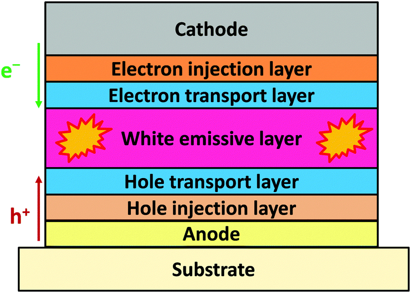 | ||
| Fig. 1 Conventional device structure of a bottom-emitting WOLED. | ||
In terms of device performance, the most important parameter characterizing an OLED is its EQE, which is defined as the ratio between the actually emitted photons from the device and the amount of injected charge carriers. As shown in Fig. 2, the EQE of an OLED can be formulated as
| ηEQE = γηS/TΦPLηout |
:3 under electrical operation.15–17 For fluorescent emitters, the radiative decay of triplet excitons (75%) is spin-forbidden, only the singlet excitons (25%) can decay radiatively for light emission (fluorescence). For phosphorescent emitters, singlet excitons in the phosphor are subject to intersystem crossing (ISC) and transfer to the triplet state, leading to the radiative decay of 100% of the excitons. ΦPL is the intrinsic PL quantum yield (PLQY) of emissive molecules, indicating the efficiency at which the spin-allowed excitons decay radiatively rather than by a non-radiative mechanism; ηout is the light out-coupling efficiency representing the ratio of photons finally coming out from the device. Under ideal conditions, the numbers of electrons and holes injected into the EML are equal (γ = 1) and all of them can recombine to generate excitons within the EML. Moreover, all the generated singlet and triplet excitons can be used to excite emissive molecules for radiative decay (ηS/T = 1, ΦPL = 1), thus leading to an internal quantum efficiency (IQE) of 100%. Finally, all the generated photons are able to leave the OLED stack to the outside for an EQE = 100%.
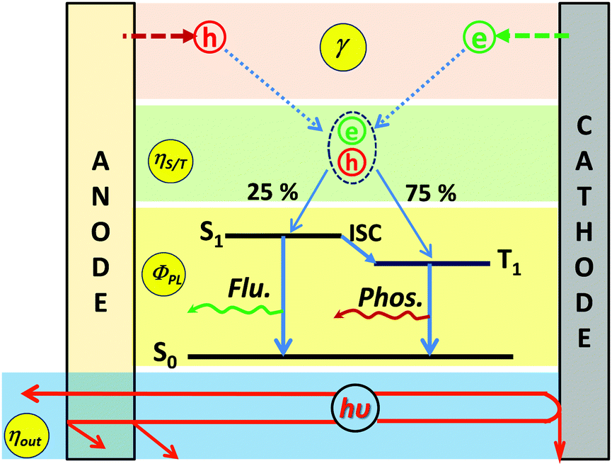 | ||
| Fig. 2 Schematic luminance processes with factors that affect the EQE in a typical OLED. | ||
However, in most WOLEDs, the different charge injection barriers and mobilities for electrons and holes, the excited state interactions as well as interactions with charge carriers (e.g. triplet–triplet annihilation, triplet–polaron quenching), and the higher refractive index of the OLED layer than the glass substrates and air make it challenging to achieve the ideal conditions for highly efficient WOLEDs. In principle, the device efficiency can be optimized through the maximization of each parameter in the EQE equation. Against these challenges, recent advances will be discussed below.
3. Charge balance for WOLEDs
Effective control of the charge balance is critical for high-performance OLED devices. Charge unbalancing in the injection and transport processes leads to an excess of one type of charge carrier accumulating at the hetero-interfaces in OLEDs, resulting in a loss of efficiency and reduced lifetime.18Fig. 3 depicts the charge distribution in an OLED. To achieve high efficiency, an EML should be ideally in the charge recombination zone where the number of holes and electrons are equal, which can be accomplished by adjusting the thickness of the HTL and the ETL.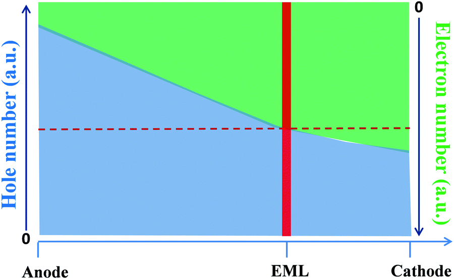 | ||
| Fig. 3 Schematic diagram of charge distribution in an OLED without considering interface affection, the number of holes and electrons in the EML are equal under the ideal conditions (γ = 1). | ||
An OLED containing a single organic material, namely the homojunction architecture,19 is an attractive device structure due to its simplicity for device fabrication. The most simple structure to realize a balanced homojunction OLED is using an ambipolar host material which has similar charge mobility for holes and electrons. Qiao et al. demonstrated such homojunction OLEDs comprising an ambipolar host material 2,5-bis-2-9H-carbazol-9-ylphenyl-1,3,4-oxadiazole (o-CzOXD) doped with iridium complexes. For the single layer OLEDs, balanced charge carriers in the EML are realized with the help of hole-trapping and the electron-transporting role of the iridium complexes.20 For example, in the green OLED with 9 wt% Ir(ppy)3 doped with o-CzOXD, holes are mainly trapped at the dopant sites prior to passing through the doping region, resulting in a reduced hole mobility, while electron transport is even enhanced by the additional transporting channel on Ir(ppy)3 molecules. All these procedures improve the charge balance in the emissive region in the high electrical field.
Wang et al. further improved the charge injection and transport characteristics in a homojunction OLED with o-CzOXD. Homojunction top-emitting devices are composed of a MoO3-doped host as the HTL, and a Cs2CO3-doped host as the ETL. EMLs consist of a host doped with (ppy)2Ir(acac), (fbi)2Ir(acac) and (PPQ)2Ir(acac) for green, orange and red emission, respectively (Fig. 4). Top-emitting OLEDs with even higher efficiency than multi-layer heterojunction bottom-emitting devices were obtained.21 Although few reports on such homojunction WOLEDs have been reported, they show promising and feasible routes for practical application of homojunction WOLEDs.
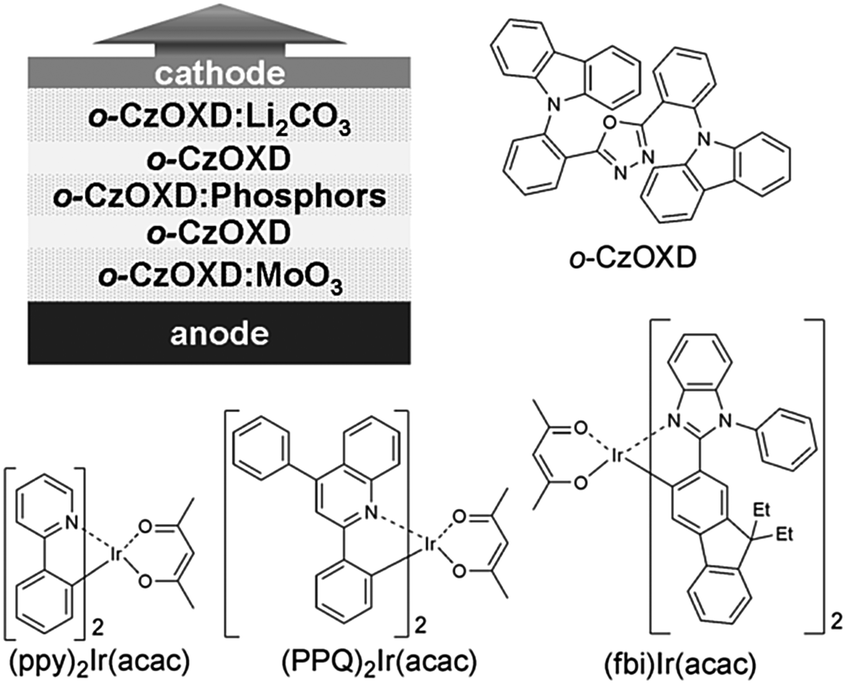 | ||
| Fig. 4 Schematic architecture of the p–i–n homojunction top-emitting OLEDs and the host and dopants used by Wang et al. Reprinted with the permission from ref. 21. Copyright 2011 Wiley-VCH. | ||
In commonly used multi-layer heterojunction OLEDs, the charge balance is determined by charge injection and transport in devices. The efficient and balanced charge injection and transport should meet the following requirements: (1) the materials should possess suitable ionization potentials and electron affinities for energy level matching to ensure efficient injection at the interfaces between electrode/organic and organic/organic materials, and (2) the materials should have a high carrier mobility and the ability to form a high-quality morphological film. Fig. 5 shows the commonly used hole transport materials (HTMs) and electron transport materials (ETMs) with their charge carrier mobility illustrated in Tables 1 and 2, respectively. The electron mobility (μe) of ETMs are very close to the hole mobility (μh) of HTMs, which has allayed the widely recognized concern that HTMs usually have a hole mobility that is about 3 orders of magnitude higher than the electron mobility of ETMs.18 As the electron mobility has been greatly improved by the development of novel ETMs, the charge carrier balance can be brought close to unity by using doped transport layers and exciton confined structures in small-molecule OLEDs.22 For example, Zhu et al. proposed a p–i–n white OLED with TCTA:MoO3 as the HTL and BmPyPB:Cs2CO3 as the ETL. By adjusting the doping concentration of MoO3 and Cs2CO3, well balanced charge injection and transport were realized, together with high T1 of TCTA and BmPyPB to confine triplet excitons in the EML, white emission with the forward viewing EQE of 22.0% and the CRI of 83 at 1000 cd m−2 was achieved.23
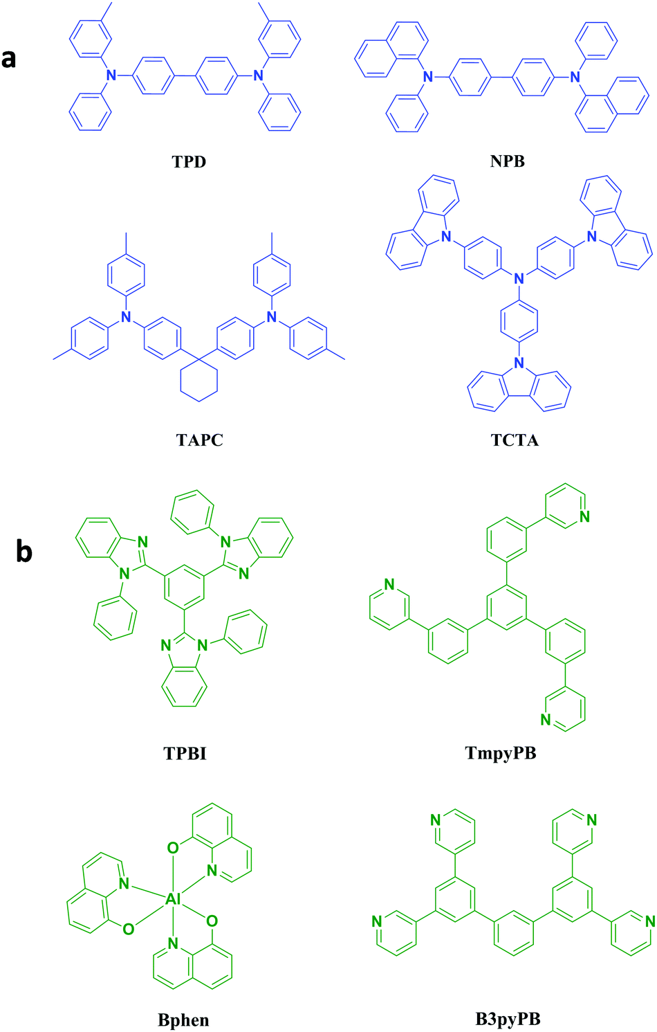 | ||
| Fig. 5 Typical HTMs (a) and ETMs (b) in small-molecule OLEDs. | ||
In a typical heterojunction OLED, a p-type host usually shifts the recombination zone to the ETL, while an n-type host shifts it to the HTL. A mixed host with p- and n-type materials can be employed to adjust the charge balance and broaden the charge recombination zone. Zhao et al. employed a fluorescent/phosphorescent hybrid WOLED by using mixed TCTA and Bepp2 as the host of phosphorescent EMLs and the interlayer (Fig. 6). The charge carrier distribution can be well controlled by adjusting the ratio of TCTA:Bepp2 in the red and green EML and the interlayer. Therefore, the efficiency roll-off was greatly improved due to the broadened exciton distribution zone.32
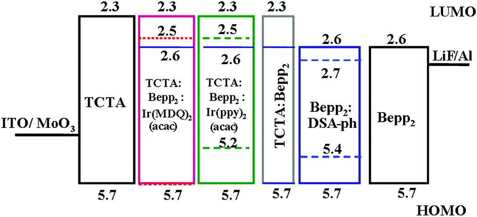 | ||
| Fig. 6 Device structure of a WOLED using a mixed host to adjust charge carriers. Reprinted with permission from ref. 32. Copyright 2012 Elsevier. | ||
4. Emissive materials and devices for WOLEDs
Assuming that balanced charge is possible for efficient OLEDs and that all the charges recombine in the EML, considerations on quantum statistics ηS/T are crucial for the realization of devices exhibiting high efficiencies. In order to realize efficient OLEDs, both singlet and triplet excitons have to be harvested for the generation of photons. The development of OLEDs has been enabled by and will continue to rely on the availability of tailor-made OLED emissive materials. Currently, there are three main emissive materials available to harvest excitons: fluorescence, phosphorescence as well as thermally activated delayed fluorescence (TADF) materials. A schematic overview of these mechanisms is shown in Fig. 7.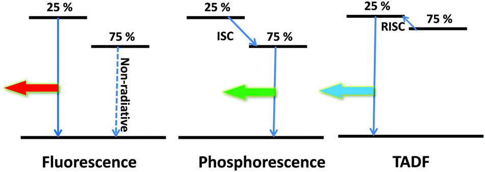 | ||
| Fig. 7 Schematic mechanism of fluorescence, phosphorescence and TADF. | ||
Conventional fluorescent molecules have a relatively large energy difference (singlet–triplet splitting) between the S1 and T1 states. This difference results in an exciton utilization of 25% from the radiative decay of singlet excitons, while 75% of triplet excitons are quenched by competing nonradiative processes (e.g. triplet–triplet annihilation or vibronic relaxation), making the conventional fluorescent OLEDs inefficient with an upper limit EQE of only 25%, so the conventional all-fluorescent WOLEDs are not discussed in this review.
4.1 Phosphorescent materials and Ph-WOLEDs
With the heavy transition-metals such as iridium, platinum, and osmium in phosphorescent molecules,33,34 the spin–orbit coupling interaction is significantly enhanced, which enables fast and efficient intersystem crossing from the excited singlet state (S1) to the triplet state (T1), theoretically leading to an IQE of 100%.35,36 Since the pioneering work of Baldo et al. showing that phosphorescent emitters can greatly improve the OLED efficiency,33 considerable scientific effort has provided numerous phosphorescent materials for OLEDs reaching impressive EQEs. Fig. 8 shows the molecular structures of typical and efficient red, green, and blue phosphorescent emitters. For example, an EQE of 21% and a CIE of (0.62, 0.37) with the EL spectrum peaking at 605 nm were reported by Jeon et al. using a red dopant bis(2-phenylquinoline)(acetylacetonate)iridium [Ir(phq)2(acac)] in a narrow band-gap fluorescent host material, bis(10-hydroxybenzo[h]quinolinato)beryllium complex (Bebq2).37 Chen et al. obtained an efficient deep red OLED with an EQE of 21.4% and a power efficiency of 24.1 lm W−1 with the spectrum peaking at 620 nm by employing a deep red emitter Ir(piq)3 in the host 9-(4-(6-(9H-carbazol-9-yl)-4-phenylquinolin-2-yl)phenyl)-9H-carbazole (CzPPQCz), and they also reported a highly efficient OLED with an orange-red emitter tris(2-phenylquinoline)iridium(III) [Ir(pq)3] in the 9-(4-(4-phenylquinolin-2-yl)phenyl)-9H-carbazole (CzPPQ) host, which achieved an EQE of 25.6% and a power efficiency of 68.1 lm W−1 with a spectrum centered at 580 nm.38 For green and yellow phosphorescent OLEDs, significant advances have been made by the development of material design and device technology. Helander et al. reported anEQE of 29.2% (79 lm W−1) at 1000 cd m−2 for a green OLED with Ir(ppy)2(acac) doped in CBP as the emitter based on a chlorinated ITO substrate with a work function of >6.1 eV.39 Fan et al. reported a yellow OLED with a maximum EQE of 25.7% (69 lm W−1) with a yellow iridium phosphor (Bt)2Ir(acac). Blue phosphorescent materials also show very high efficiency.40 In 2014, the Kido group reported a maximum EQE and a power efficiency of 21.7% and 50.1 lm W−1, respectively, by using a typical sky blue emitter FIrpic as the dopant.41 The energy transfer from the exciplex formed at the interface of TAPC and 5′,5′′′′-sulfonyl-di-1,1′:3′,1′′-terphenyl (BTPS) to the dopant was attributed to the high efficiency. In the same year, they reported a greenish-blue OLED using a tris-cyclometallated iridium complex with a phenylimidazole-based ligand, fac-tris(mesityl-2-phenyl-1H-imidazole)iridium(III) [fac-Ir(mpim)3] as the emitter, the optimized device showed an extremely high EQE of 29.6%, and a power efficiency of 75.6 lm W−1 at 100 cd m−2. Lee and co-workers developed deep blue Ph-OLEDs with a maximum EQE above 25.1% by doping the iridium(III) complex bis((3,5-difluoro-4-cyanophenyl)pyridine)iridium picolinate (FCNIrpic) in a bipolar host material 9-(3-(9H-carbazole-9-yl)phenyl)-3-(dibromophenylphosphoryl)-9H-carbazole (mCPPO1) and a high triplet energy exciton-blocking material diphenylphosphine oxide-4-(triphenylsilyl)phenyl (TSPO1).42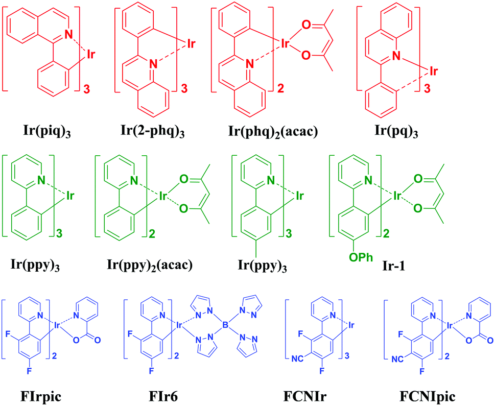 | ||
| Fig. 8 Molecular structure of typical red, green and blue phosphorescent emitters. | ||
Benefitting from the development of phosphorescent materials, the efficiencies of phosphorescent WOLEDs (Ph-WOLEDs) have been greatly improved. Su et al. reported highly efficient white OLEDs with ultrathin (0.25 nm) orange EMLs between blue phosphorescent EMLs. Efficient exothermic energy transfer from the triplet states of TCTA and DCzPPy to that of FIrpic was realized, resulting in an excellent triplet energy confinement on the blue emitter FIrpic. The yellow emission was enabled by efficient energy transfer from triplet states of the host materials and FIrpic to those of the PQ2Ir. A record power efficiency of 44 lm W−1 at 1000 cd m−2 luminance in the forward direction was achieved without using any out-coupling techniques.43
Wang et al. reported an efficient Ph-WOLED by incorporating FIrpic for blue emission and (fbi)2Ir(acac) for orange emission in a single EML (Fig. 9a). The emissive mechanisms of FIrpic and (fbi)2Ir(acac) were demonstrated to be different in two parallel channels: host–guest energy transfer for blue emission and direct exciton formation for yellow emission, respectively. Unfavorable energy losses are therefore greatly reduced. The operational principle of the WOLEDs is depicted in Fig. 9b. By precisely managing all the electrically generated excitons, the resulting WOLEDs can achieve a peak forward-viewing power efficiency of 42.5 lm W−1, corresponding to an EQE of 19.3%.44
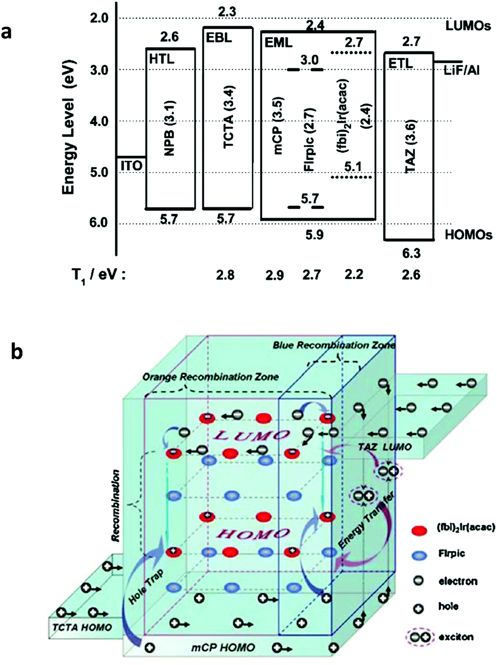 | ||
| Fig. 9 (a) Energy diagram and device structure of the all-phosphor dual-color WOLEDs. The numbers in parentheses indicate the energy gaps of the materials. (b) Proposed operational principle of the Ph-WOLEDs. Reproduced with permission from ref. 44. Copyright 2009 Wiley-VCH. | ||
Doping free OLEDs have attracted substantial interest due to the simplicity of the fabrication process. For ultrathin un-doped WOLEDs, the thickness and position of the ultrathin un-doped EML are very critical in the efficient utilization of the generated excitons. Zhu et al. reported a highly efficient Ph-WOLED with an ultrathin un-doped orange EML sandwiched between two blue EMLs.45 In order to achieve high efficiency, two blue EMLs with the hole-transport host TCTA and the bipolar-transport host 26DCzPPy were employed, respectively. The thickness of the ultrathin un-doped orange EML has been optimized to adjust energy transfer from the blue emitter to the yellow emitter. The optimized WOLEDs show a power efficiency of 53.4 lm W−1, and an EQE of 22.2% at 1000 cd m−2 in the forward-view direction with low efficiency roll-off. And it also exhibits ideal warm-white EL spectra with the CIE coordinates of (0.41, 0.44) at a practical brightness of 1000 cd m−2.
Besides high efficiency, a long operational lifetime is also essential for WOLED technology to achieve practical application. After more than a decade of research, significant breakthroughs in the lifetime of green and red Ph-OLEDs have been achieved, with the reported half lifetime (T50) from 1000 cd m−2 higher than 106 h.46,47 However, the operational stability of all Ph-WOLEDs remains a significant challenge due to the significantly shorter lifetime of blue phosphorescent emitters. In contrast to their red and green counterparts, these blue Ph-OLEDs retain lifetimes on the order of a few tens to hundreds of hours.48–51 The degradation mechanism of these shorter lifetime blue Ph-OLEDs has been attributed in part to energetically driven formation of traps formed due to bimolecular triplet–polaron quenching (TPQ).52 When a triplet exciton (∼2.8 eV) on the phosphor encounters a polaron (∼3.3 eV) on a nearby host molecule, the exciton will be quenched, and the polaron is excited to a higher energy level (>6 eV).53 This high-energy polaron in blue emitting materials is sufficiently high to break up and degrade the emissive molecules through bond cleavage. As an example, the commonly used sky-blue emitter, FIrpic, is subjected to broken Ir–O bonds after excitation, followed by the loss of CO2 and the formation of FIrpic+.54 The long lifetime (microsecond scale)55 of triplet states in phosphorescent OLEDs increases the likelihood of these destructive events, especially in contrast to the likelihood of these events occurring in fluorescent emitters with significantly shorter exciton lifetimes (nanoseconds).56 The Forrest group reported a novel blue phosphorescent device with a graded dopant concentration profile in a broadened emissive layer to suppress TPQ, resulting in a lifetime of 616 ± 10 hours (time to degradation to 80% of the initial 1000 cd m−2 initial luminance), representing the most efficient sky-blue phosphorescent FIrpic emitter.7 However, this reported lifetime still lags far behind the practical values, due to the intrinsic chemical degradation of blue phosphorscent emitters.48,57
4.2 Hybrid WOLEDs with conventional blue fluorescent materials
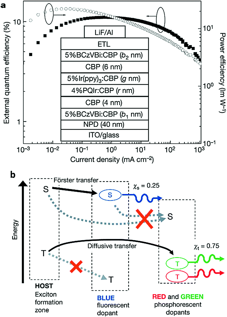
In contrast, blue fluorescent OLEDs have shown sufficient reliability for practical use. Therefore, a combination of a blue fluorescent emitter with red and green (or yellow) phosphorescent emitters is considered to be an ideal solution to realize long lifetime fluorescence–phosphorescence hybrid WOLEDs. Furthermore, in the hybrid white OLEDs, the blue fluorescent emitter can harvest 25% of singlet excitons and the other 75% of triplet excitons are harvested in the phosphorescent EMLs, which can theoretically achieve an IQE of 100%.58Inspired by the phosphor sensitized fluorescent monochrome OLEDs,59,60 hybrid WOLEDs have been reported for more than ten years.61–63 However, a substantial breakthrough in device efficiency was not achieved until 2006, when Sun et al. proposed a smart architecture by placing an ambipolar spacer layer CBP between fluorescent and phosphorescent EMLs, as shown in Fig. 10a. The device exhibited a maximum total EQE of 18.7 ± 0.5% and a maximum total power efficiency of 37.6 ± 0.6 lm W−1.64 Two exciton formation regions were formed at the interfaces between carrier transport layers (HTL for hole and ETL for electron) and blue fluorescent EMLs. As the design concept shown in Fig. 10b, the singlet excitons with shorter diffusion length are harvested by the fluorescent emitter 4,40-bis(9-ethyl-3-carbazovinylene)-1,10-biphenyl (BCzVBi), while the triplet excitons can migrate to red and green phosphorescent EMLs for radiative decay due to the long diffusion length of triplet excitons (460 ± 30 Å). Although the singlet and triplet excitons are effectively separated, CBP molecules with a lower triplet energy than that of the blue emitter serve as triplet traps which quench a considerable amount of triplet excitons, resulting in a forward EQE of only 10% at 500 cd m−2.
 | ||
| Fig. 10 (a) Device structure for a hybrid WOLED based on the concept of separating fluorescent and phosphorescent EMLs by a spacer layer. (b) Proposed energy transfer mechanism in this device. Reproduced with permission from Ref. 64. Copyright 2006 Nature Publishing Group. | ||
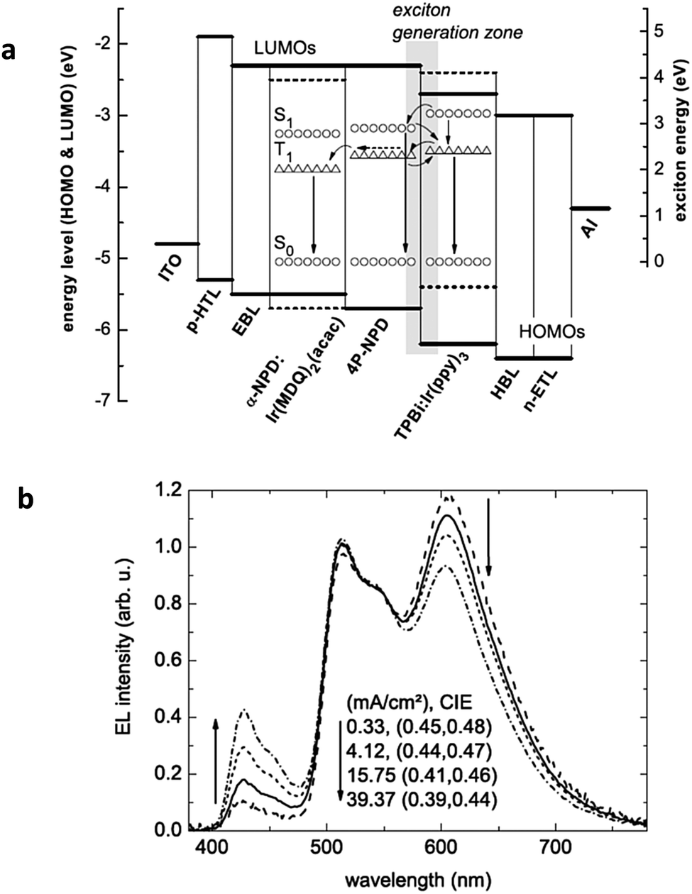
Moreover, the use of the interlayer in hybrid WOLEDs has several disadvantages that limit the device efficiency. Firstly, the voltage drop across the interlayer is not negligible, leading to lower power efficiency. Moreover, the interlayer brings additional interfaces which could induce energy losses by increasing the possibility of charge imbalance and exciplex formation.58 Finally, the additional fabrication step for an interlayer is also unfavorable for commercial applications. To mitigate the aforementioned issue, Schwartz and co-workers employed a blue fluorophore with high triplet energy between red and green phosphorescent EMLs to harvest triplet excitons.65 The device structure and possible exciton transfer mechanisms are shown in Fig. 11a. The key feature in this WOLED is that the blue fluorophore 4P-NPD with a high triplet state (2.3 eV) can effectively avoid trapping triplets by transferring them to the adjacent phosphorescent EMLs, while the singlet excitons are directly used for blue fluorescence within this layer. Based on this triplet harvesting concept, highly efficient hybrid WOLEDs with reduced efficiency roll-off were achieved. By the introduction of a p-doped HTL and an n-doped ETL, the device can achieve a power efficiency of 22.0 lm W−1, corresponding to 10.4% EQE at 1000 cd m−2. The triplet harvesting concept inspired subsequent work on hybrid WOLEDs; some fluorophores with high triplet energy were synthesized to be multi-functional as blue emitters and phosphorescent hosts, and hybrid WOLEDs with simpler structures were developed.66–68
 | ||
| Fig. 11 (a) Device structure of hybrid WOLEDs and possible exciton transfer mechanisms proposed by Schwartz et al. (b) EL spectra of the hybrid WOLEDs at different current densities. Reproduced with permission from ref. 65. Copyright 2007 Wiley-VCH. | ||
Owing to the relatively lower triplet energy of 4P-NPD (2.3 eV) compared to that of Ir(ppy)3 (2.5 eV), a possible Dexter energy transfer from the triplet state of Ir(ppy)3 to the lower lying non-radiative triplet state of 4P-NPD may occur, which results in energy loss and thus the obtained device efficiency is far behind the expected value for the hybrid WOLEDs in ref. 66. Moreover, the shifting of the recombination zone with increased driving voltage leads to unstable white spectra at different brightnesses (Fig. 11b), which is also a common issue for hybrid WOLEDs.
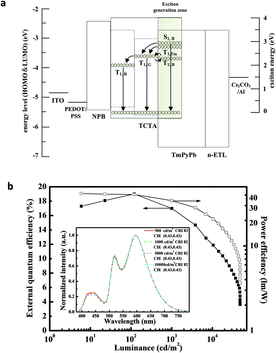
Sun et al. suppressed the aforementioned intrinsically mutual quenching between the fluorescent emitter and the phosphorescent emitter by introducing mixed hosts with bipolar-transport properties to construct the blue fluorescent EML, and Ir(ppy)2(acac) with lower triplet energy (2.4 eV) as the green emitter (Fig. 12a).69 The optimized device exhibits impressive EL performances with a turn-on voltage of 3.1 V. The maximum forward-view EQE, current efficiency, and power efficiency of the device are 19.0%, 45.2 cd A−1, and 41.7 lm W−1, respectively. And at the practical brightness of 1000 cd m−2, they still retain 17.0%, 40.5 cd A−1, and 34.3 lm W−1, exhibiting less pronounced efficiency roll-off. The EL spectra of the hybrid WOLED turned out to be stable within the investigated brightness ranges (Fig. 12b). The above advantages are attributed to the broad exciton recombination zone within the EML owing to the ambipolar transporting properties of the mixture of TCTA and TmPyPb, as well as the efficient utilization of excitons in the blue emissive zone at a low blue dopant concentration.
 | ||
| Fig. 12 (a) Energy level diagram and energy transfer scheme in hybrid WOLEDs proposed by Sun et al. (b) EL performance of the hybrid WOLED; inset: normalized EL spectra of the hybrid WOLED at different current densities. Reproduced with permission from ref. 69. Copyright 2014 Wiley-VCH. | ||
4.3 Hybrid WOLEDs with blue TADF materials
Except for phosphorescent emitters, TADF is another material that enables the harvesting of both triplet and singlet excitons for light emission.15 TADF materials have shown very high efficiency in OLEDs because they can theoretically harvest all the singlet and triplet excitons, through a reverse intersystem crossing (RISC) process from the triplet state to the singlet state due to the low ΔEST, which is typically several hundred meV and could be as low as 0.01 eV,70 leading to an efficient RISC process. As shown in Fig. 13, efficient red, green and blue TADF emissive materials have been reported71–73 after the monumental breakthrough on TADF OLEDs by Adachi and co-workers in 2012.72 Since the efficiency of hybrid OLEDs with conventional fluorescent materials is still far behind the expected values, WOLEDs based on highly efficient blue TADF emitters can potentially achieve a comparable device efficiency to that of all phosphorescent WOLEDs. | ||
| Fig. 13 Molecular structures of highly efficient TADF emissive materials. | ||
In 2014, Duan et al. reported the first hybrid WOLEDs with 4,5-bis(carbazol-9-yl)-1,2-dicyanobenzene (2CzPN) as the blue TADF emitter to suppress the intrinsically mutual quenching between the fluorescent emitter and the phosphorescent emitter(s). By wisely taking advantage of the energy levels of the materials and the trapping ability of the dopant, the devices exhibit stable warm emission with a maximum forward viewing EQE of 22.6% and a power efficiency (PE) of 47.1 lm W−1.74 As the external heavy-atom effect of the phosphors may quench the conventional fluorescence due to the increased singlet–triplet ISC rate constant and the radiative or non-radiative decay rate of triplet excitons in the fluorophores, Duan et al. found that the TADF fluorophore is much less sensitive to the external heavy-atom effect perturber than the conventional fluorophores due to the almost unchanged ISC rate and the enhanced rate of reverse ISC. By doping a yellow phosphor and a blue fluorophore with TADF into a single EML, hybrid WOLEDs with a maximum forward-viewing EQE of 19.6% and a maximum forward-viewing power efficiency of 50.2 lm W−1 are achieved.75
Recently, Wu et al. demonstrated high-performance TADF-based hybrid WOLEDs by employing a TADF molecule DMAC-DPS as the blue emitter combined with red and green phosphorescent emitters.76Fig. 14a shows the device structure and the operational mechanism of the resulting hybrid R–G–B WOLEDs. Due to the high triplet energy of DMAC-DPS, cascaded energy transfer from the blue emitter to the green and then the red emitter contributes to efficient utilization of excitons. The EL performance of the resulting WOLEDs is also dependent on the doping concentration of Ir(ppy)2(acac); therefore, the regulation of doping concentration facilitates the precise manipulation of charges and excitons, leading to efficient hybrid WOLEDs with a forward-viewing maximum EQE, current efficiency, and power efficiency of 23.0%, 51.0 cd A−1, and 51.7 lm W−1, respectively, which are even comparable to those of the state-of-the-art all phosphorescent WOLEDs. Moreover, the EL spectra exhibit remarkable colour stability with a high CRI of 89, CIE coordinates of (0.438, 0.438) and a CCT of 3231 K at 1000 cd m−2 (Fig. 14b).
 | ||
| Fig. 14 (a) Proposed energy diagram of hybrid WOLEDs with a blue TADF molecule. (b) EL performance of hybrid WOLEDs with a blue TADF molecule; inset: normalized EL spectra of the hybrid WOLED at different luminance. Reproduced with permission from ref. 76. Copyright 2016 Wiley-VCH. | ||
In addition to the utilization of TADF materials, the exciplex with the TADF effect has recently drawn substantial attention. Chen et al. demonstrated an efficient blue exciplex system formed by a new hole transport material (4-dimesitylboryl)phenyltriphenylamine (TPAPB) and a commonly used electron transport material TPBi. The resulting exciplex exhibited a high photoluminescence quantum yield of 44.1%. Using only these two organic materials, a high performance blue-emitting OLED was fabricated with a spectral peak at 468 nm and a maximum EQE of 7.0 ± 0.4%. Furthermore, a yellow phosphorescent dopant Ir(2-phq)3 was doped in the above exciplex system with a low concentration of 0.5 wt%, and a WOLED with a power efficiency of 25.1 ± 0.1 lm W−1 and an EQE of 14.0 ± 0.2 at 100 cd m−2 was obtained.77
Liu et al. reported an efficient TADF exciplex system formed in a mixed film comprising a hole-transporting molecule 4,40-bis(9-carbazolyl)-2,20-dimethylbiphenyl (CDBP) and an electron-transporting molecule ((1,3,5-triazine-2,4,6-triyl)tris(benzene-3,1-diyl))tris(diphenylphosphine oxide) (POT2T).78 Both CDBP and PO-T2T have PL emission peaks smaller than 400 nm, whereas the CDBP:PO-T2T mixed film shows a broad and significantly red-shifted PL spectrum with a peak at 476 nm, which is attributed to exciplex emission. By doping green phosphor Ir(ppy)2(acac)) and red phosphor Ir(MDQ)2(acac) into the blue TADF exciplex, they fabricated a hybrid WOLED with a maximum EQE and power efficiency of 25.5% and 84.1 lm W−1, respectively. Although the device achieved high maximum efficiencies, they decreased to 14.8%, and 24.2 lm W−1 at 1000 cd m−2, exhibiting severe efficiency roll-off, and the EL spectra showed an obvious color change with increased luminance with a CRI of 76.
The overall EL performances of hybrid WOLEDs with blue TADF emitters surpass those with conventional fluorescent emitters, and even are comparable to those of all phosphorescent WOLEDs. Even so, they still suffer from some big challenges. In the TADF mechanism, triplet excitons must be converted into luminescent singlet excitons for fluorescence via a reverse intersystem crossing (RISC) mechanism. This additional process before fluorescence emission delays the luminescence process, resulting in an increased fluorescence lifetime of up to several microseconds.72 Due to the inherently long delayed lifetime of TADF molecules, the probability of the exciton quenching processes such as singlet–triplet annihilation (STA), triplet–triplet annihilation (TTA), and exciton–polaron quenching progressively increases with increasing luminance, leading to severe efficiency roll-off at high brightness. This roll-off in efficiency directly correlates with degradation in lifetime as evidenced by the previously mentioned, state of the art blue TADF emitter, DMAC-DPS, with the lifetime of approximately one hour.79 Moreover, to date, deep blue TADF molecules are very rare. Though continual innovation will slowly improve the performance and lifetime of TADF materials, the aforementioned issues currently limit the use of blue TADF materials from practical applications in WOLEDs.
4.4 TADF-sensitized fluorescent WOLEDs
The conventional fluorescent emitters, which are composed of simple aromatic compounds, have continued to attract interest because of their long operational lifetimes, broader freedom of molecular design and potential to be manufactured at low cost in next-generation full-color display and lighting applications. However, conventional fluorescent OLEDs have suffered from low EQEs with a limitation of 25%, making it a major concern for the application of fluorescent OLEDs. TADF sensitized fluorescence is a new triplet harvesting strategy to overcome the EQE limitation for conventional fluorescent emitters. The formed triplet excitons on the TADF molecules can be converted into singlet excitons so that all of the exciton energy is transferred to the fluorescent molecules as singlet excitons, leading to highly efficient emission.Recent conceptual advances based on TADF sensitization such as the TADF-assisted dopant and the sensitizing TADF host have been proposed to boost triplet harvesting. Adachi et al. employed TADF molecules as assistant dopants with a wide-energy-gap host and conventional fluorescent emitters in fluorescent OLEDs in which TADF dopants are separated from fluorescent dopants by host molecules to prevent Dexter energy transfer between them that will cause energy losses. As a result, maximum EQEs of 13.4%, 15.8%, 18.0% and 17.5% were achieved for blue, green, yellow and red OLEDs.80 This concept was extended to WOLEDs by employing a blue TADF emitter bis[4-(9,9-dimethyl-9,10-dihydroacridine)phenyl]sulfone (DMACDPS) as the exciton donor and green and red fluorescent emitters dispersing in the host mCP as exciton acceptors. The exciton donor and acceptors are separated into two different layers with a 2 nm spacer layer inserted between them, causing carrier recombination mainly on the blue TADF molecules. The generated singlet excitons either directly or by RISC can be resonantly transferred to the red and green fluorescent acceptors through the spacer layer, which eliminates direct carrier recombination on fluorescent dopants, leading to a WOLED with an EQE of 12% and a CIE of (0.25, 0.31).81
According to Fermi's Golden rule,82 small singlet–triplet splitting (ΔEST) for realizing efficient reverse ISC usually conflicts with the fast radiative decay rate for high PLQY in TADF emitters. Duan et al. directly used TADF materials as sensitizing hosts to excite fluorescent dopants, which breaks the trade-off between small ΔEST and high radiative decay rates, leading to a high-efficiency orange-fluorescent OLED with a EQE of 12.2%.83
Ma et al. demonstrated high-efficiency fluorescent WOLEDs with low efficiency roll-off employing DMAC-DPS as the host for a conventional orange fluorescent emitter. Concentration of the dopant was optimized to prevent energy loss from the Dexter energy transfer from the triplet energy of the TADF host to that of the dopant.84 The resulting WOLEDs using DMAC-DPS as the host exhibit excellent EL performances with the maximum forward viewing power efficiency and EQE of 48.0 lm W−1 and 14.0%, respectively. At a practical brightness of 1000 cd m−2, they remain as high as 29.3 lm W−1, and 13.0%, indicating a much improved efficiency roll-off compared with the TADF emitters-based WOLEDs. Fluorescent WOLEDs with DMAC-DPS as the TADF assistant dopant were also studied in this work, showing inferior performance to the TADF host devices, which is attributed to the broad exciton distribution in the TADF host with its ambipolar transport properties. The exciton recombination zone in the WOLEDs using DMAC-DPS as the host with its ambipolar-transporting properties. Based on the sensitizing TADF host concept, Ma et al. also demonstrated efficient R–G–B fluorescent WOLEDs by emissive layer design to manipulate charges and excitons in the emissive regions, leading to very high performance of over 18% EQE and stable EL spectra with a high CRI of 82 for the reported fluorescent WOLEDs.85
Since all fluorescent WOLEDs are attracting more and more interest due to their long operational lifetime, high color purity, and potential to be manufactured at low cost in next-generation display and lighting applications. It seems that TADF-sensitized fluorescent WOLEDs with high efficiency, good reliability, and low efficiency roll-off would offer a new avenue for the future development of high-performance WOLEDs. However, serving as the fluorescent sensitizer as well as blue emitters, operationally stable blue TADF materials still face challenges.
5. Light out-coupling
The light extraction efficiency is defined as the fraction of photons generated in the EML that escape into free space from OLED devices, which is a key factor affecting the EQE. When light passes from a material of high refraction index to one of low refraction index, there is an angle at which the light starts to be reflected at the interface of the materials, which is described quantitatively by Snell's Law. In conventional OLEDs, the emitted light at a wide incident angle tends to be trapped in the high-refractive-index layers such as the organic medium, ITO and glass substrate due to total internal reflection instead of being able to escape, resulting in low light extraction efficiency. In addition, the excitation of surface plasmons at the interface to the metallic cathode further reduces the light extraction efficiency.86 Therefore, even for OLEDs with an internal quantum efficiency of nearly 100%, the upper limit of EQE is typically around 20–25%.87Fig. 15 shows the different optical channels for anisotropic emissive molecules when being excited in a standard OLED stack corresponding to the substrate mode, the waveguide mode and the surface plasmon (SP) mode, respectively. Effective approaches for enhancing light extraction are desired for OLEDs with a more improved EQE than 20% and various methods have been devised to overcome the EQE limitation of OLEDs. | ||
| Fig. 15 Optical channels in a conventional OLED with anisotropic emissive molecules. | ||
5.1 Light out-coupling for the substrate mode
Due to the large difference of refractive indices of glass substrates (nglass ∼ 1.5) and air (nair = 1), the light incident at the substrate/air planar interface with an angle larger than the critical angle is subjected to total internal reflection. It is then guided in the so-called substrate modes, damped due to the limited reflectivity of the underlying stack, and can escape through the edges of the device.88Numerous substrate modification techniques have been implemented to enhance light extraction from the substrate mode. The most commonly used method is to attach a light scattering film to the back-surfaces or using microlense to prohibit the total internal reflection at the glass/air interface by increasing the critical angle.89,90 Möller et al. employed microlens arrays with 10 mm diameter poly-dimethyl-siloxane lenses attached to the glass substrates of a green OLED, which widens the escape cone for total internally reflected light incident at the air–substrate boundary. Thus the extraction of light at angles higher than the critical angle of glass is enhanced, resulting in a factor of 1.5 enhancement over unlensed substrates.91 Chen et al. proposed a very simple and cost-effective method to roughen the substrate surface by simply sand-blasting the edges and back-side surface of the glass substrates, 20% enhancement of forward efficiency has been achieved due to the light scattering effect.90 Lee et al. reported another simple method using O2 plasma treatment on the back side of a PET substrate to form a sub-micrometer-sized pattern (Fig. 16), which contributes to a 70% enhancement of luminance by improving light extraction from the substrate to air.92
 | ||
| Fig. 16 Spontaneously formed nanopatterns on polymer films for flexible OLEDs. Reproduced with permission from ref. 92. Copyright 2015 Wiley-VCH. | ||
5.2 Light out-coupling for the waveguide mode
In typical OLEDs, the total thickness of the organic layers is generally limited to 100–200 nm, which is below or comparable with the wavelength of the emitted photons. Light emitted under large angles is totally reflected at the interface between the glass and the anode, which is attributed to the large difference of refractive indices between the glass substrate (nglass ∼ 1.5) and organic layers (norganic ∼ 1.8) as well as ITO (nITO ∼ 1.8). Consequently, the light is waveguided between the glass/anode interface and the reflecting cathode, and may finally be parasitically absorbed in the organic layers or leave the device through the edges.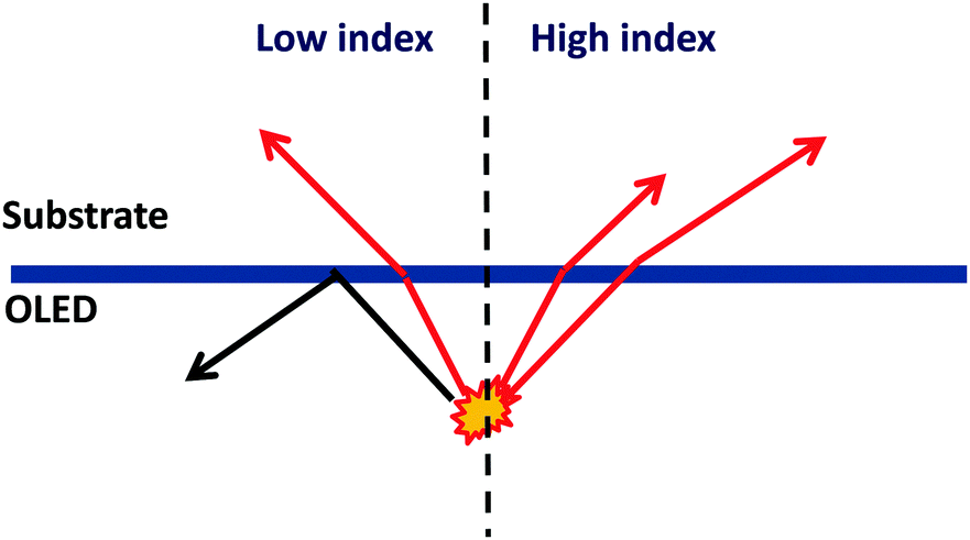 | ||
| Fig. 17 Schematic light extraction of the waveguide mode in OLEDs with a high index substrate compared to that with a low index substrate. | ||
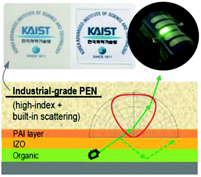
However, it should be noted that it is rather costly to obtain glass substrates with a high refractive index, which is partly due to instability in the glass forming process and lower chemical durability with lower contents of SiO2. A high index polymer film is a good substitute for high index glasses.98 Kim et al. employed an industrial-grade version of polyethylene naphthalate (PEN) as the high index substrate (n ∼ 1.7) for OLEDs, another high index polymer polyamide-imide (PAI) was coated on PEN to provide a smooth surface for preparing indium zinc oxide (IZO) and a relatively good index matching between PEN and IZO (Fig. 18). As a result, waveguided modes were effectively extracted to the substrate. Combined with built-in scattering properties of PEN which enables the extraction of those substrate-confined modes to the air without any substrate structuring or additional microlens array films, a green OLED with an EQE of 29.6% (98.7 lm W−1) was achieved with an enhancement factor of 1.32.99
 | ||
| Fig. 18 Device structure of OLEDs with the high-index substrate reported by Kim et al. Reproduced with permission from ref. 99. Copyright 2015 Wiley-VCH. | ||
 | ||
| Fig. 19 Scheme of intensity distribution of the waveguide mode in the light-emitting devices with a light scattering layer. Reproduced with permission from ref. 100. Copyright The Royal Society of Chemistry 2015. | ||
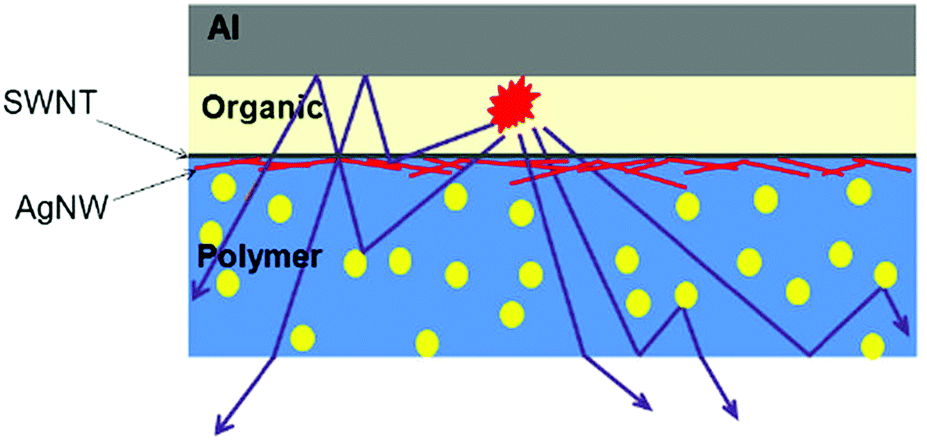
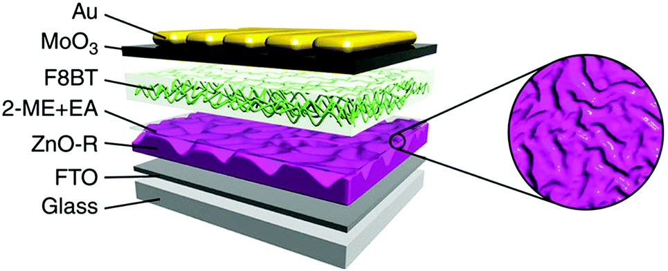
Li et al. demonstrated a light scattering layer with nanoparticles of barium strontium titanate dispersed in a polymer, single-walled carbon nanotubes and silver nanowires stacked and embedded in the surface of the scattering layer to form the transparent electrode (Fig. 20). Based on the flexible substrates with a scattering layer, a 2.5 fold enhancement of the current efficiency at 10000 cd m−2 was reported for green and white polymer OLEDs.101
 | ||
| Fig. 20 Schematic illustration of light scattering by nanoparticles in the SWNT/Ag NW-nanocomposite substrate. Reprinted with permission from ref. 101. Copyright Nature Publishing Group 2014. | ||
Kumar et al. fabricated a nanostructured ITO (NSITO) between a conducting anode and a glass substrate using a glancing angle deposition method by radio frequency (RF) sputter. The refractive index of the scattering layer varies from 1.2 to 1.9 depending on the deposition angle. OLEDs with these films inserted between glass and conducting ITO were found to have enhanced out-coupling efficiency in comparison to the reference OLED by about 80%.102
It is not easy to control the random scattering center of the internal scattering layers discussed above, which makes them not exactly reproducible. Nanoimprint lithography for the nanostructure is another choice for developing light extracted substrates. Using an ultraviolet (UV) curable polymer resin and UV nanoimprint lithography, Jeon et al. fabricated two-dimensional nanostructural pillars with a UV curable resin and SiNx on the glass substrate directly (Fig. 21) and 50% enhancement of the EL intensity was achieved compared with the conventional device.103 Moreover, OLEDs with the pillars in the substrates exhibit interesting emission patterns depending on the symmetry and dimensions of the pillars.
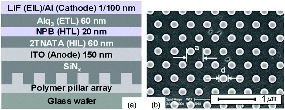 | ||
| Fig. 21 (a) Vertical structure and materials of OLEDs with a 2D nanostructure in the substrate. (b) SEM image of the imprinted polymer pillars. Reproduced with permission from ref. 103. Copyright American Institute of Physics 2016. | ||
In 2008, the Forrest group fabricated a low-refractive-index grid (n = 1.45) using standard photolithographic methods between ITO and the organic layers, which allowed redirecting light traveling and improving extraction of waveguided light into the glass and air modes. Combined with microlens arrays on the substrate surface, an out-coupling enhancement of ∼2.3 times over that using a conventional flat glass substrate was achieved.104 Recently they demonstrated a non-diffractive dielectric grid layer between ITO and the glass substrate using photolithographic methods (Fig. 22), which couples out all waveguide mode power into the substrate with a minimal impact on the wavelength, the viewing angle and molecular dipole alignment.105 Importantly, because the grid lies below the anode, its design and fabrication are completely independent of the PHOLED structure and performance. This characteristic of the sub-anode grid allows the complete freedom in materials and device structure needed to achieve a fully optimized emitting device.
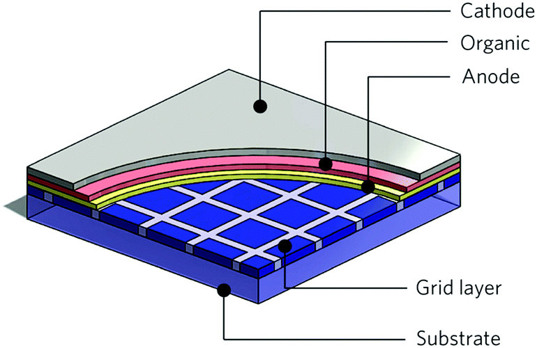 | ||
| Fig. 22 Schematic cut-away view of an OLED with a sub-anode grid. Reprinted with permission from ref. 105. Copyright Nature Publishing Group 2015. | ||
Lee et al. demonstrated a spontaneously formed ripple-shaped nanostructure of ZnO for an inverted PLED (Fig. 23) through the reorganization of gel particles of zinc acetate dihydrate [Zn(CH3COO)22H2O] during the slow drying process. As a result, the out-coupling efficiency of 79% was achieved when the ripple period was ∼300 nm, which is primarily attributed to the reduction in the in-plane wave vectors of the waveguide modes caused by the Bragg grating vector.110 Except for the extraction of the waveguide mode, the surface plasmon mode should also be reduced by the periodical cathode morphology.
 | ||
| Fig. 23 Device architecture of inverted PLEDs with a ripple-shaped structure. Reprinted with permission from ref. 110. Copyright Nature Publishing Group 2014. | ||
5.3 Surface plasmon mode
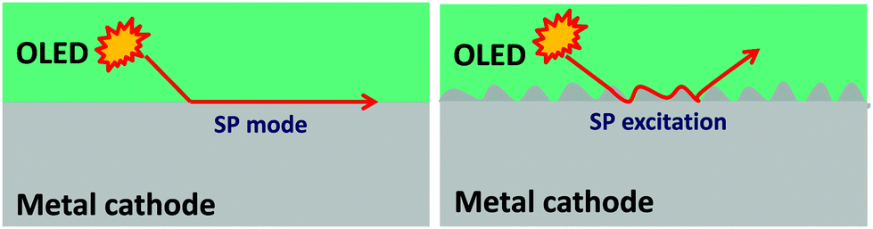
As long as substrate modes and waveguide modes are extracted to the air, the remaining loss in OLEDs is due to the quenching of excitons by surface plasmon (SP) modes associated with the metallic cathode. Surface plasmons are waves that propagate along the surface of a conductor.111 The emitters in close proximity to the thin cathode metal efficiently couple their optical energy into SP modes at the interface of the metal cathode and the organic material, where the SP fraction can be up to 40% of the total radiation.112,113 In a conventional bottom-emitting OLED with a thick metal cathode, the SP modes are mainly distributed between the bottom surface of the metal and the ETL, therefore making it difficult to manipulate the extraction of SP modes from the outside of devices. However, they can be reduced or extracted by several approaches.Since the coupling to SP modes is a near-field effect, the amount of dissipated power depends on the distance to the metal. Therefore increasing the distance between the emitter and the cathode is a simple method to reduce the coupling between emitting dipoles and the SP mode. In 2010, Leo's group simulated the quantification of energy loss channels as a function of ETL thickness in a red phosphorescent OLED. As shown in Fig. 24, the SP mode is notably extracted to the waveguide mode with increasing ETL thickness, reaching a negligible level for thicknesses >200 nm.114 The thick ETL involves an n-doped transport layer to maintain electrical characteristics. Qu et al. used a 240 nm ETL with Bphen:Cs separating the EML from the Al planar electrode, which showed an operating voltage comparable to conventional devices at the same luminance. Due to the reduced SP modes, the thick ETL contributes to a 50% increase in the EQE.105
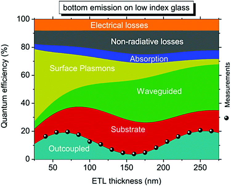 | ||
| Fig. 24 Simulation of the distribution of energy loss channels in a red bottom OLED, as well as measured EQE as a function of the ETL thickness and comparison to simulation results. Reprinted with permission from ref. 114. Copyright American Institute of Physics 2010. | ||
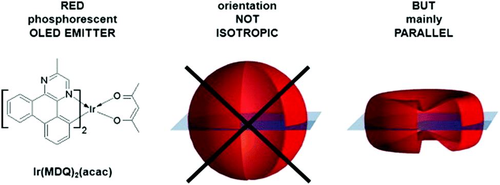
As the increased ETL thickness reduces the SP modes by shifting them to waveguide modes rather than extracting them out, no significant increase of the overall efficiency is implemented only with a thick ETL. Therefore, waveguide mode extraction should be accompanied by SP mode shifting to realize high out-coupling efficiency. A more promising approach for a strongly reduced coupling to SP modes is the employment of oriented emitters that have their transition dipole moment oriented parallel to the substrate plane.115 In this case, the coupling of horizontally oriented dipoles to SP modes is significantly reduced in comparison to perpendicular dipoles. A bunch of horizontally oriented fluorescent molecules with linear-shaped molecules in an isotropic host matrix film has been reported.116–118 For phosphorescent emitters which are usually bulky metal–organic complexes with isotropic dopant orientation,119,120 a non-isotropic, predominantly parallel emitter orientation in the well-known red phosphorescent emitter Ir(MDQ)2(acac) blended in an α-NPD matrix (Fig. 25) was reported, and an out-coupling efficiency increase of ∼50% compared to the isotropic case was achieved,121 demonstrating a promising approach for light out-coupling in phosphorescent guest–host systems. Kim et al. demonstrated that the green phosphorescent emitter Ir(ppy)2(acac) has a preferred non-isotropic orientation with a horizontal to vertical dipole ratio of 0.77:0.23 in their device, resulting in an EQE of 30% for the green OLEDs.122
 | ||
| Fig. 25 Predominantly parallel emitter orientation in Ir(MDQ)2(acac): α-NPD. Reprinted with permission from ref. 121. Copyright 2011 Elsevier. | ||
Transparent metal-free OLEDs are other optimal devices used for significantly reducing power dissipation into SP modes.123 Lee et al. proposed a transparent green OLED with a 60 nm IZO as the anode and a 70 nm ITO as the cathode. Without interaction between the metal surface and the emitting dipoles, SP modes in the transparent OLED are significantly reduced. By integrating a micro-cone array on one side and a half-sphere lens on the other side, a total EQE of 62.9% was achieved for the green phosphorescent OLED.124
Instead of a typical planar metal layer with heavy SP loss, a corrugated metal layer can extract SP modes by being Bragg-scattered into visible light. The dispersion of SP modes traveling between two semi-infinite layers is described in Fig. 26. Since the wave vector of SP modes is larger than the in-plane wave vector of light for all frequencies, no coupling between SPs and light is possible in the case of planar interfaces. Therefore, in a device such as an OLED where an emitting dye molecule excites SPs from the optical near field, power that is coupled to SPs is dissipated as heat and therefore lost. A periodically corrugated microstructure allows Bragg scattering of SPP modes, thus SPP modes can be shifted partly into the light cone.
 | ||
| Fig. 26 Schematic dispersion SP modes in an OLED with a planar and corrugated structure. | ||
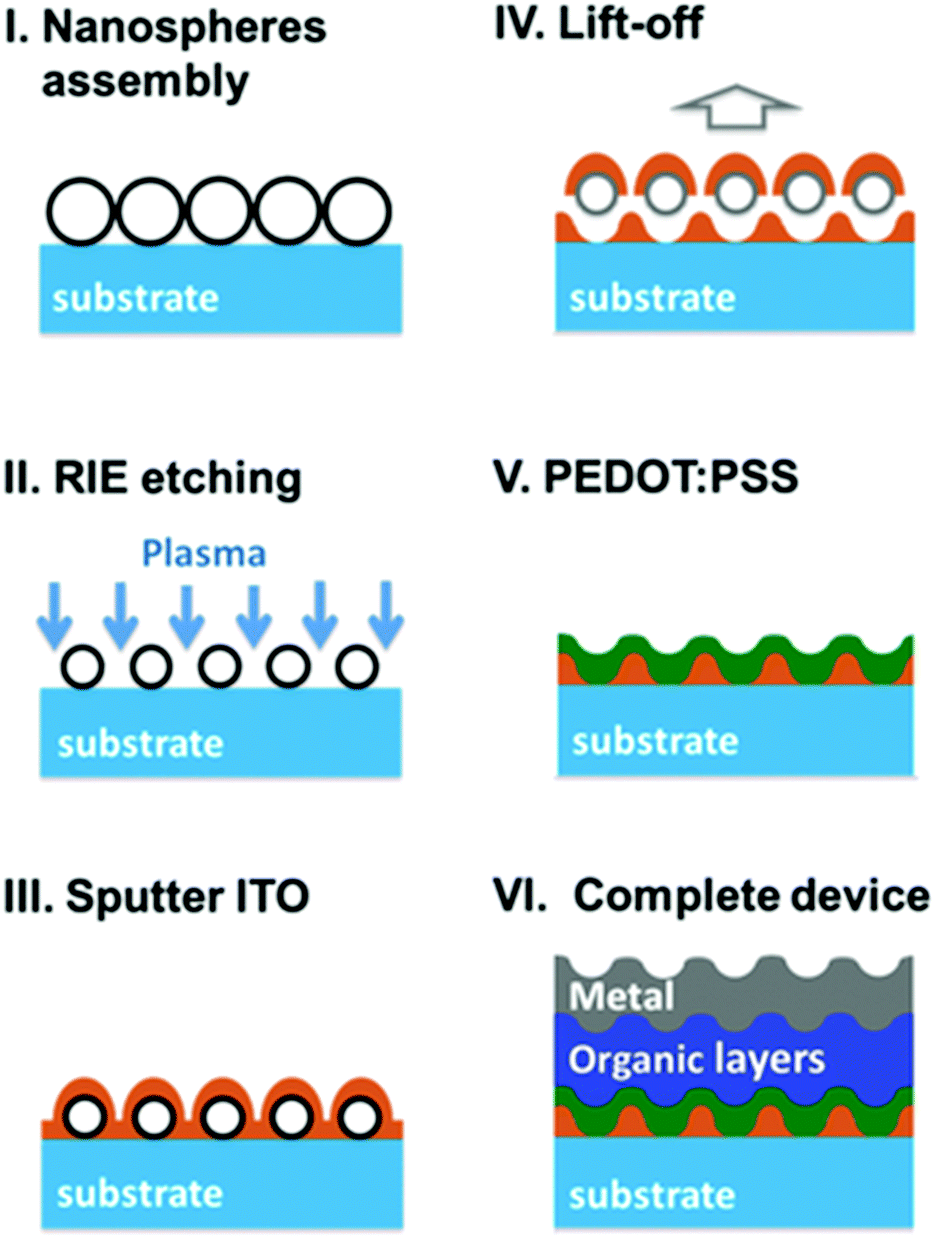
Bi et al. demonstrated a corrugated red OLED with integrating dual-periodic corrugation by employing a laser interference lithography technique. The light trapped in the SPP modes associated with both top and bottom electrode/organic interfaces is efficiently extracted from the OLEDs by adjusting appropriate periods of two set corrugations, and a 29% enhancement in the current efficiency has been obtained.125 Chen et al. reported a facile method to fabricate an ITO nanomesh by nanosphere lithography. As shown in Fig. 27, firstly a polystyrene (PS) self-assembled monolayer was fabricated on a glass substrate. The diameter of PS nanospheres was reduced from 500 nm to ∼270 nm after reactive ion (RIE) etching. ITO was then deposited on the PS monolayer. The ITO nanomesh was obtained by removing (lifting off) PS nanospheres and excess ITO on nanospheres. As a result, the corrugated OLED including the corrugated metal cathode was obtained based on the ITO nanomesh, which significantly reduces SP losses for radiation from the vertical dipoles. In addition, making use of very different refractive indices of ITO mesh and PEDOT:PSS, internal extraction was further enhanced. By combining this internal extraction structure and the attached extraction lens, a very high EQE of nearly 62% (264.3 lm W−1) was achieved with a green phosphorescent OLED.126
 | ||
| Fig. 27 Schematic diagram and EL performances of an ITO nanomesh OLED reported by Chen et al. Reproduced with permission from ref. 126. Copyright 2015 Wiley-VCH. | ||
6. Highly efficient WOLEDs with light out-coupling
By combining the energy efficient device architecture with the improved light out-coupling concept for WOLEDs, the power efficiency surpassed 100 lm W−1. In 2014, Zhou et al. reported a phosphorescent WOLED with Firpic and PO-01 as the blue and yellow emitters, respectively (Fig. 28).127 By nanoimprinting the PEDOT:PSS layer with deterministic periodic nanostructures and applying a microlens array to the anode using plastic with embedded Ag networks (PEAN), the flexible white OLEDs exhibit a maximum EQE of 49% and a record power efficiency of 106 lm W−1 at 1000 cd m−2.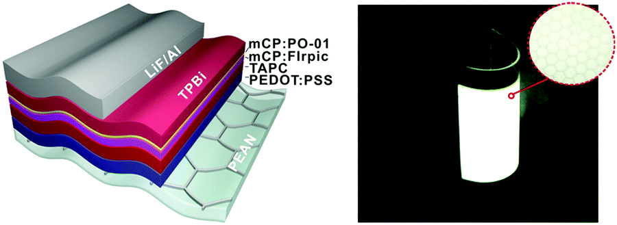 | ||
| Fig. 28 Schematic device structure and photograph for the flexible white OLEDs using PEAN as the anode. Reproduced with permission from ref. 127. Copyright © 2014 American Chemical Society. | ||
By employing the internal extraction structure comprising a high refractive-index layer and a light scattering layer to extract the waveguide modes, and using an external extraction structure to extract the substrate modes, Konica Minolta Inc. demonstrated all-phosphorescent WOLEDs with a state of the art power efficiency of 130 lm W−1 (CCT = 2857 K) at 1000 cd m−2 in 2015, even at 5000 cd m−2, the WOLED still maintains 110 lm W−1,128 indicating a highly meaningful step for WOLEDs to enter into the general lighting market.
7. Conclusions
We have reviewed different approaches to fabricate highly efficient small-molecule WOLEDs including charge balance technology, efficient and stable emissive materials, device architecture, and light out-coupling techniques. Plenty of related efforts have been made to realize a high efficiency, high colour-quality, reliable stability, simple and low-cost fabrication procedure as well as the trade-off among these parameters for WOLEDs. Continued breakthroughs including a very high efficiency of 100 lm W−1 have been achieved. However, there are still some challenges preventing the widespread manufacture of WOLEDs: high efficiency and operationally stable blue emissive materials, device lifetime and efficiency roll-off at high luminance in WOLEDs, and realizing high light out-coupling efficiency with simple approaches.The merits of WOLEDs such as high efficiency, low driving voltage, flexibility, and low energy consumption have made them the most promising candidate for the next-generation full-colour displays and solid-state lighting sources. Flexible WOLEDs will be the ultimate choice in the smart display and lighting industry, because of their advantages including portability and large-size and low-cost production. However, the reliability of flexible WOLEDs by the limitation of the transparent electrode on the flexible substrate and the encapsulation method still need to be further improved.
To date, the most efficient WOLEDs are grown in high-vacuum systems using thermal evaporation sources. New manufacturing techniques like roll-to-roll, inject printing and slot-die coating offer better choices for mass production of low-cost WOLEDs, and these processes may eventually make the cost of producing WOLEDs competitive, especially for polymeric WOLEDs. However, their luminous efficiency remains a big challenge compared with small-molecule WOLEDs.
Appendix A
International Union of Pure and Applied Chemistry (IUPAC) names of the materials abbreviation discussed in this paper.| Abbreviation | IUPAC name of material |
|---|---|
| Ir(ppy)3 | fac-Tris(2-phenylpyridine)iridium(III) |
| Ir(ppy)2(acac) | Bis(2-phenylpyridinato-N,C20)iridium (acetylacetonate) |
| (fbi)2Ir(acac) | Bis(2-(9,9-diethyl-fluoren-2-yl)-1-phenyl-1H-benzo[d]imidazolato)(actylacetonate)iridium(III) |
| (PPQ)2Ir(acac) | Bis(2,4-diphenylquinolyl-N,C2′)iridium(acetylacetonate) |
| Ir(2-phq)3 | Tris(2-phenylquinoline)iridium(III) |
| PO-01 | (Acetylacetonato)bis[2-(thieno[3,2-c]pyridin-4-yl)phenyl]iridium(III) |
| Ir(bt)2(acac) | Bis(2-phenyl benzothiozolato-N,C20)iridium (acetylacetonate) |
| Ir(MDQ)2(acac) | Bis(2-methyldibenzo[f,h]quinoxaline) (acetylacetonate)iridium(III) |
| FIrpic | Bis(3,5-diuoro-2-(2-pyridyl)phenyl-(2-carboxypyridyl)iridium(III) |
| Fir6 | Bis(2,4-diuorophenylpyridinato)tetrakis(1-pyrazolyl)borate iridium(III) |
| 4P-NPD | N,N′-Di-(1-naphthalenyl)-N,N′-diphenyl-[1,10:40,1′′:4′′,1000-quaterphenyl]-4,4000-diamine |
| CBP | 4,4′-Bis(N-carbazolyl)-1,1′-biphenyl |
| TPD | N,N′-Bis(3-methylphenyl)-N,N′-diphenylbenzidine |
| NPB | N,N′-Di(1-naphthyl)-N,N′-diphenyl-(1,1′-biphenyl)-4,4′-diamine |
| TCTA | 4,40,4′′-Tris(carbazol-9-yl)-triphenylamine |
| TAPC | 1,10-Bis[4-(di-p-tolylamino)phenyl]cyclohexane |
| DCzppy | 2,6-Bis(3-(9H-carbazol-9-yl)phenyl)pyridine |
| 26DCzppy | 2,6-Bis(3-(9H-carbazol-9-yl)phenyl)pyridine |
| Bepp2 | Bis(2-(2-hydroxyphenyl)-pyridine)beryllium |
| TPBi | 2,20,2′′-(1,3,5-Benzenetriyl)tris-[1-phenyl-1H-benzimidazole] |
| TmPyPB | 1,3,5-Tri(m-pyrid-3-yl-phenyl)benzene |
| Bphen | 4,7-Diphenyl-1,10-phenanthroline |
| BmPyPB | 1,3-Bis(3,5-dipyrid-3-yl-phenyl)benzene |
| DPEPO | Bis[2-(diphenylphosphino)phenyl]ether oxide |
| DMAC-DPS | Bis[4-(9,9-dimethyl-9,10-dihydroacridine)phenyl]sulfone |
Acknowledgements
The authors gratefully acknowledge the National Key R&D Program of China (2016YFB0400700), and the National Natural Science Foundation of China (Grant No. 51333007, 91433201, 11661131001) for the support of this research.Notes and references
- M. Pope, H. Kallmann and P. Magnante, J. Chem. Phys., 1963, 38, 2042–2043 CrossRef CAS.
- C. W. Tang and S. A. Van Slyke, Appl. Phys. Lett., 1987, 51, 913–915 CrossRef CAS.
- B. W. D'Andrade and S. R. Forrest, Adv. Mater., 2004, 16, 1585–1595 CrossRef.
- C.-T. Chen, Chem. Mater., 2004, 16, 4389–4400 CrossRef CAS.
- F. So, J. Kido and P. Burrows, MRS Bull., 2008, 33, 663–669 CrossRef CAS.
- Y. Tao, C. Yang and J. Qin, Chem. Soc. Rev., 2011, 40, 2943–2970 RSC.
- W. Song, I. Lee and J. Y. Lee, Adv. Mater., 2015, 27, 4358–4363 CrossRef CAS PubMed.
- K. Suzuki, S. Kubo, K. Shizu, T. Fukushima, A. Wakamiya, Y. Murata, C. Adachi and H. Kaji, Angew. Chem., 2015, 127, 15446–15450 CrossRef.
- http://www.oled-info.com/samsung-display-demonstrates-rollable-oled .
- http://www.oled-info.com/oled-watch .
- http://www.oled-info.com/auos-38-90hz-amoled-vr-application-now-production .
- http://www.lgoledlight.com/index.do# .
- http://https://www.oledworks.com .
- http://www.konicaminolta.com/oled/products/index.html .
- C. Adachi, M. A. Baldo, M. E. Thompson and S. R. Forrest, J. Appl. Phys., 2001, 90, 5048–5051 CrossRef CAS.
- C. J. Chiang, A. Kimyonok, M. K. Etherington, G. C. Griffiths, V. Jankus, F. Turksoy and A. P. Monkman, Adv. Funct. Mater., 2013, 23, 739–746 CrossRef CAS.
- R. Weiner, Nanoelectronics and Information Technology: Advanced Electronic Materials and Novel Devices, Wiley-VCH, 2005 Search PubMed.
- N. Chopra, J. Lee, Y. Zheng, S.-H. Eom, J. Xue and F. So, ACS Appl. Mater. Interfaces, 2009, 1, 1169–1172 CAS.
- H. Tsuji, C. Mitsui, Y. Sato and E. Nakamura, Adv. Mater., 2009, 21, 3776–3779 CrossRef CAS.
- X. Qiao, Y. Tao, Q. Wang, D. Ma, C. Yang, L. Wang, J. Qin and F. Wang, J. Appl. Phys., 2010, 108, 034508 CrossRef.
- Q. Wang, Y. Tao, X. Qiao, J. Chen, D. Ma, C. Yang and J. Qin, Adv. Funct. Mater., 2011, 21, 1681–1686 CrossRef CAS.
- M. Pfeiffer, S. R. Forrest, K. Leo and M. E. Thompson, Adv. Mater., 2002, 14, 1633–1636 CrossRef CAS.
- L. Zhu, Z. Wu, J. Chen and D. Ma, J. Mater. Chem. C, 2015, 3, 3304–3310 RSC.
- A. Kuwahara, S. Naka, H. Okada and H. Onnagawa, Appl. Phys. Lett., 2006, 89, 132106 CrossRef.
- W. S. Jeon, J. S. Park, L. Li, D. C. Lim, Y. H. Son, M. C. Suh and J. H. Kwon, Org. Electron., 2012, 13, 939–944 CrossRef CAS.
- C. W. Lee and J. Y. Lee, Org. Electron., 2014, 15, 399–404 CrossRef CAS.
- J.-W. Kang, S.-H. Lee, H.-D. Park, W.-I. Jeong, K.-M. Yoo, Y.-S. Park and J.-J. Kim, Appl. Phys. Lett., 2007, 90, 223508 CrossRef.
- W.-Y. Hung, T.-H. Ke, Y.-T. Lin, C.-C. Wu, T.-H. Hung, T.-C. Chao, K.-T. Wong and C.-I. Wu, Appl. Phys. Lett., 2006, 88, 064102 CrossRef.
- S. J. Su, T. Chiba, T. Takeda and J. Kido, Adv. Mater., 2008, 20, 2125–2130 CrossRef CAS.
- S. Naka, H. Okada, H. Onnagawa and T. Tsutsui, Appl. Phys. Lett., 2000, 76, 197–199 CrossRef CAS.
- T. Kamata, H. Sasabe, Y. Watanabe, D. Yokoyama, H. Katagiri and J. Kido, J. Mater. Chem. C, 2016, 4, 1104–1110 RSC.
- F. Zhao, Z. Zhang, Y. Liu, Y. Dai, J. Chen and D. Ma, Org. Electron., 2012, 13, 1049–1055 CrossRef CAS.
- M. A. Baldo, D. O'brien, Y. You, A. Shoustikov, S. Sibley, M. Thompson and S. Forrest, Nature, 1998, 395, 151–154 CrossRef CAS.
- R. C. Evans, P. Douglas and C. J. Winscom, Coord. Chem. Rev., 2006, 250, 2093–2126 CrossRef CAS.
- L. Xiao, S. J. Su, Y. Agata, H. Lan and J. Kido, Adv. Mater., 2009, 21, 1271–1274 CrossRef CAS.
- E. L. Williams, K. Haavisto, J. Li and G. E. Jabbour, Adv. Mater., 2007, 19, 197–202 CrossRef CAS.
- W. S. Jeon, T. J. Park, S. Y. Kim, R. Pode, J. Jang and J. H. Kwon, Org. Electron., 2009, 10, 240–246 CrossRef CAS.
- C.-H. Chen, L.-C. Hsu, P. Rajamalli, Y.-W. Chang, F.-I. Wu, C.-Y. Liao, M.-J. Chiu, P.-Y. Chou, M.-J. Huang and L.-K. Chu, J. Mater. Chem. C, 2014, 2, 6183–6191 RSC.
- M. Helander, Z. Wang, J. Qiu, M. Greiner, D. Puzzo, Z. Liu and Z. Lu, Science, 2011, 332, 944–947 CrossRef CAS PubMed.
- C. Fan, L. Zhu, B. Jiang, Y. Li, F. Zhao, D. Ma, J. Qin and C. Yang, J. Phys. Chem. C, 2013, 117, 19134–19141 CAS.
- Y. Seino, H. Sasabe, Y. J. Pu and J. Kido, Adv. Mater., 2014, 26, 1612–1616 CrossRef CAS PubMed.
- S. O. Jeon, S. E. Jang, H. S. Son and J. Y. Lee, Adv. Mater., 2011, 23, 1436–1441 CrossRef CAS PubMed.
- S. J. Su, E. Gonmori, H. Sasabe and J. Kido, Adv. Mater., 2008, 20, 4189–4194 CAS.
- Q. Wang, J. Ding, D. Ma, Y. Cheng, L. Wang, X. Jing and F. Wang, Adv. Funct. Mater., 2009, 19, 84–95 CrossRef CAS.
- L. Zhu, Y. Zhao, H. Zhang, J. Chen and D. Ma, J. Appl. Phys., 2014, 115, 244512 CrossRef.
- J. Birnstock, T. Canzler, M. Hofmann, A. Lux, S. Murano, P. Wellmann and A. Werner, J. Soc. Inf. Disp., 2008, 16, 221–229 CrossRef CAS.
- S. Madasamy, D. Pavicic, C. Rothe, S. Murano, J. Birnstock, J. Blochwitz-Nimoth, S. Mladenovski, K. Neyts and M. Pfeiffer, Proc. SPIE, 2008, 6999, 69991E CrossRef.
- R. Seifert, I. R. de Moraes, S. Scholz, M. C. Gather, B. Lüssem and K. Leo, Org. Electron., 2013, 14, 115–123 CrossRef CAS.
- Y. Zhang, J. Lee and S. R. Forrest, Nat. Commun., 2014, 5, 5008 CrossRef CAS PubMed.
- J.-A. Seo, S. K. Jeon, M. S. Gong, J. Y. Lee, C. H. Noh and S. H. Kim, J. Mater. Chem. C, 2015, 3, 4640–4645 RSC.
- P.-C. Huang, M.-H. Chang, J.-S. Lin, H.-C. Yeh and M.-R. Tseng, SID Symposium Digest of Technical Papers, 2016, p. 47.
- N. Giebink, B. D'Andrade, M. Weaver, J. Brown and S. Forrest, J. Appl. Phys., 2009, 105, 124514 CrossRef.
- N. Giebink, B. D'Andrade, M. Weaver, P. Mackenzie, J. Brown, M. Thompson and S. Forrest, J. Appl. Phys., 2008, 103, 044509 CrossRef.
- I. R. de Moraes, S. Scholz, B. Lüssem and K. Leo, Appl. Phys. Lett., 2011, 99, 053302 CrossRef.
- K. S. Yook and J. Y. Lee, Adv. Mater., 2012, 24, 3169–3190 CrossRef CAS PubMed.
- S. J. Yeh, M. F. Wu, C. T. Chen, Y. H. Song, Y. Chi, M. H. Ho, S. F. Hsu and C. H. Chen, Adv. Mater., 2005, 17, 285–289 CrossRef CAS.
- I. R. de Moraes, S. Scholz, B. Lüssem and K. Leo, Org. Electron., 2011, 12, 341–347 CrossRef.
- G. Schwartz, S. Reineke, T. C. Rosenow, K. Walzer and K. Leo, Adv. Funct. Mater., 2009, 19, 1319–1333 CrossRef CAS.
- M. Baldo, M. Thompson and S. Forrest, Nature, 2000, 403, 750–753 CrossRef CAS PubMed.
- B. W. D'Andrade, M. A. Baldo, C. Adachi, J. Brooks, M. E. Thompson and S. R. Forrest, Appl. Phys. Lett., 2001, 79, 1045–1047 CrossRef.
- F. Li, G. Cheng, Y. Zhao, J. Feng, S. Liu, M. Zhang, Y. Ma and J. Shen, Appl. Phys. Lett., 2003, 83, 4716–4718 CrossRef CAS.
- D. Qin and Y. Tao, Appl. Phys. Lett., 2005, 86, 3507 CrossRef.
- J.-F. Li, S.-F. Chen, S.-H. Su, K.-S. Hwang and M. Yokoyama, J. Electrochem. Soc., 2006, 153, H195–H197 CrossRef CAS.
- Y. Sun, N. C. Giebink, H. Kanno, B. Ma, M. E. Thompson and S. R. Forrest, Nature, 2006, 440, 908–912 CrossRef CAS PubMed.
- G. Schwartz, M. Pfeiffer, S. Reineke, K. Walzer and K. Leo, Adv. Mater., 2007, 19, 3672–3676 CrossRef CAS.
- T. Peng, Y. Yang, H. Bi, Y. Liu, Z. Hou and Y. Wang, J. Mater. Chem., 2011, 21, 3551–3553 RSC.
- F. Zhao, N. Sun, H. Zhang, J. Chen and D. Ma, J. Appl. Phys., 2012, 112, 084504 CrossRef.
- C. J. Zheng, J. Wang, J. Ye, M. F. Lo, X. K. Liu, M. K. Fung, X. H. Zhang and C. S. Lee, Adv. Mater., 2013, 25, 2205–2211 CrossRef CAS PubMed.
- N. Sun, Q. Wang, Y. Zhao, Y. Chen, D. Yang, F. Zhao, J. Chen and D. Ma, Adv. Mater., 2014, 26, 1617–1621 CrossRef CAS PubMed.
- K. Sato, K. Shizu, K. Yoshimura, A. Kawada, H. Miyazaki and C. Adachi, Phys. Rev. Lett., 2013, 110, 247401 CrossRef PubMed.
- J. Li, T. Nakagawa, J. Macdonald, Q. Zhang, H. Nomura, H. Miyazaki and C. Adachi, Adv. Mater., 2013, 25, 3319–3323 CrossRef CAS PubMed.
- H. Uoyama, K. Goushi, K. Shizu, H. Nomura and C. Adachi, Nature, 2012, 492, 234–238 CrossRef CAS PubMed.
- M. Taneda, K. Shizu, H. Tanaka and C. Adachi, Chem. Commun., 2015, 51, 5028–5031 RSC.
- D. Zhang, L. Duan, Y. Li, D. Zhang and Y. Qiu, J. Mater. Chem. C, 2014, 2, 8191–8197 RSC.
- D. Zhang, L. Duan, Y. Zhang, M. Cai, D. Zhang and Y. Qiu, Light: Sci. Appl., 2015, 4, e232 CrossRef CAS.
- Z. Wu, J. Luo, N. Sun, L. Zhu, H. Sun, L. Yu, D. Yang, X. Qiao, J. Chen and C. Yang, Adv. Funct. Mater., 2016, 26, 3306–3313 CrossRef CAS.
- Z. Chen, X.-K. Liu, C.-J. Zheng, J. Ye, C.-L. Liu, F. Li, X.-M. Ou, C.-S. Lee and X.-H. Zhang, Chem. Mater., 2015, 27, 5206–5211 CrossRef CAS.
- X. K. Liu, Z. Chen, J. Qing, W. J. Zhang, B. Wu, H. L. Tam, F. Zhu, X. H. Zhang and C. S. Lee, Adv. Mater., 2015, 27, 7079–7085 CrossRef CAS PubMed.
- Q. Zhang, B. Li, S. Huang, H. Nomura, H. Tanaka and C. Adachi, Nat. Photonics, 2014, 8, 326–332 CrossRef CAS.
- H. Nakanotani, T. Higuchi, T. Furukawa, K. Masui, K. Morimoto, M. Numata, H. Tanaka, Y. Sagara, T. Yasuda and C. Adachi, Nat. Commun., 2014, 5, 4016 CAS.
- T. Higuchi, H. Nakanotani and C. Adachi, Adv. Mater., 2015, 27, 2019–2023 CrossRef CAS PubMed.
- A. Monkman, ISRN Mater. Sci., 2013, 2013, 670130 Search PubMed.
- D. Zhang, L. Duan, C. Li, Y. Li, H. Li, D. Zhang and Y. Qiu, Adv. Mater., 2014, 26, 5050–5055 CrossRef CAS PubMed.
- Z. Wu, J. Luo, N. Sun, L. Zhu, H. Sun, L. Yu, D. Yang, X. Qiao, J. Chen and C. Yang, Adv. Funct. Mater., 2016, 3306–3313 CrossRef CAS.
- Z. Wu, Q. Wang, L. Yu, J. Chen, X. Qiao, T. Ahamad, S. M. Alshehri, C. Yang and D. Ma, ACS Appl. Mater. Interfaces, 2016, 8, 28780–28788 CAS.
- L. Smith, J. Wasey and W. L. Barnes, Appl. Phys. Lett., 2004, 84, 2986–2988 CrossRef CAS.
- Y. J. Shiu, Y. C. Cheng, W. L. Tsai, C. C. Wu, C. T. Chao, C. W. Lu, Y. Chi, Y. T. Chen, S. H. Liu and P. T. Chou, Angew. Chem., Int. Ed., 2016, 55, 3017–3021 CrossRef CAS PubMed.
- G. Gomard, J. B. Preinfalk, A. Egel and U. Lemmer, J. Photonics Energy, 2016, 6, 030901 CrossRef.
- J. Shiang, T. Faircloth and A. R. Duggal, J. Appl. Phys., 2004, 95, 2889–2895 CrossRef CAS.
- S. Chen and H. S. Kwok, Opt. Express, 2010, 18, 37–42 CrossRef PubMed.
- S. Möller and S. Forrest, J. Appl. Phys., 2002, 91, 3324–3327 CrossRef.
- I. Lee, J. Y. Park, S. Gim, J. Ham, J. H. Son and J. L. Lee, Small, 2015, 11, 4480–4484 CrossRef CAS PubMed.
- L. Smith and W. Barnes, Org. Electron., 2006, 7, 490–494 CrossRef CAS.
- M.-H. Lu and J. Sturm, J. Appl. Phys., 2002, 91, 595–604 CrossRef CAS.
- S. Mladenovski, K. Neyts, D. Pavicic, A. Werner and C. Rothe, Opt. Express, 2009, 17, 7562–7570 CrossRef CAS PubMed.
- G. Gaertner and H. Greiner, Proc. SPIE 6999, Organic Optoelectronics and Photonics III, 2008, p. 69992T.
- T. Nakamura, N. Tsutsumi, N. Juni and H. Fujii, J. Appl. Phys., 2005, 97, 054505 CrossRef.
- N. Ide, K. Yamae, V. Kittichungchit, H. Tsuji, M. Ota and T. Komoda, J. Photopolym. Sci. Technol., 2014, 27, 357–361 CrossRef.
- E. Kim, H. Cho, K. Kim, T. W. Koh, J. Chung, J. Lee, Y. Park and S. Yoo, Adv. Mater., 2015, 27, 1624–1631 CrossRef CAS PubMed.
- C.-Y. Cheng, C.-W. Wang, J.-R. Cheng, H.-F. Chen, Y.-S. Yeh, H.-C. Su, C.-H. Chang and K.-T. Wong, J. Mater. Chem. C, 2015, 3, 5665–5673 RSC.
- L. Li, J. Liang, S.-Y. Chou, X. Zhu, X. Niu and Q. Pei, Sci. Rep., 2014, 4, 4307 Search PubMed.
- A. Kumar, R. Srivastava, M. Kamalasanan and D. S. Mehta, Opt. Lett., 2012, 37, 575–577 CrossRef CAS PubMed.
- S. Jeon, J.-W. Kang, H.-D. Park, J.-J. Kim, J. R. Youn, J. Shim, J.-h. Jeong, D.-G. Choi, K.-D. Kim and A. O. Altun, Appl. Phys. Lett., 2008, 92, 223307 CrossRef.
- Y. Sun and S. R. Forrest, Nat. Photonics, 2008, 2, 483–487 CrossRef CAS.
- Y. Qu, M. Slootsky and S. R. Forrest, Nat. Photonics, 2015, 9, 758–763 CrossRef CAS.
- Y. Bai, Y. Fan, Q. Lu, X. Wang, M. Chu and X. Liu, Appl. Phys. Express, 2015, 8, 022102 CrossRef.
- C.-Y. Chen, Y.-J. Chen, W.-K. Lee, C.-Y. Lu, H. Y. Lin and C.-C. Wu, Opt. Express, 2016, 24, A810–A822 CrossRef PubMed.
- J.-H. Jang, M.-C. Oh, T.-H. Yoon and J. C. Kim, Appl. Phys. Lett., 2010, 97, 123302 CrossRef.
- W. H. Koo, S. M. Jeong, F. Araoka, K. Ishikawa, S. Nishimura, T. Toyooka and H. Takezoe, Nat. Photonics, 2010, 4, 222–226 CAS.
- B. R. Lee, E. D. Jung, J. S. Park, Y. S. Nam, S. H. Min, B.-S. Kim, K.-M. Lee, J.-R. Jeong, R. H. Friend and J.-S. Kim, Nat. Commun., 2014, 5, 4840 CrossRef CAS PubMed.
- W. L. Barnes, A. Dereux and T. W. Ebbesen, Nature, 2003, 424, 824–830 CrossRef CAS PubMed.
- D. J. Gaspar and E. Polikarpov, OLED Fundamentals: Materials, Devices, and Processing of Organic Light-Emitting Diodes, CRC Press, 2015 Search PubMed.
- S. Wedge, J. Wasey, W. L. Barnes and I. Sage, Appl. Phys. Lett., 2004, 85, 182 CrossRef CAS.
- R. Meerheim, M. Furno, S. Hofmann, B. Lüssem and K. Leo, Appl. Phys. Lett., 2010, 97, 253305 CrossRef.
- J. Frischeisen, D. Yokoyama, C. Adachi and W. Brütting, Appl. Phys. Lett., 2010, 96, 073302 CrossRef.
- D. Yokoyama, A. Sakaguchi, M. Suzuki and C. Adachi, Org. Electron., 2009, 10, 127–137 CrossRef CAS.
- J. Frischeisen, D. Yokoyama, A. Endo, C. Adachi and W. Brütting, Org. Electron., 2011, 12, 809–817 CrossRef CAS.
- D. Yokoyama, J. Mater. Chem., 2011, 21, 19187–19202 RSC.
- P. Liehm, C. Murawski, M. Furno, B. Lüssem, K. Leo and M. C. Gather, Appl. Phys. Lett., 2012, 101, 3304 CrossRef.
- C. Mayr and W. Brütting, Chem. Mater., 2015, 27, 2759–2762 CrossRef CAS.
- M. Flämmich, J. Frischeisen, D. S. Setz, D. Michaelis, B. C. Krummacher, T. D. Schmidt, W. Brütting and N. Danz, Org. Electron., 2011, 12, 1663–1668 CrossRef.
- S. Y. Kim, W. I. Jeong, C. Mayr, Y. S. Park, K. H. Kim, J. H. Lee, C. K. Moon, W. Brütting and J. J. Kim, Adv. Funct. Mater., 2013, 23, 3896–3900 CrossRef CAS.
- K. Tien and C. Wu, SID Int. Symp. Dig. Tech. Pap., 2007, 38, 806–809 CrossRef CAS.
- J. B. Kim, J. H. Lee, C. K. Moon, S. Y. Kim and J. J. Kim, Adv. Mater., 2013, 25, 3571–3577 CrossRef CAS PubMed.
- Y.-G. Bi, J. Feng, Y.-S. Liu, Y.-F. Li, Y. Chen, X.-L. Zhang, X.-C. Han and H.-B. Sun, Sci. Rep., 2014, 4, 7108 CrossRef CAS PubMed.
- C. Y. Chen, W. K. Lee, Y. J. Chen, C. Y. Lu, H. Y. Lin and C. C. Wu, Adv. Mater., 2015, 27, 4883–4888 CrossRef CAS PubMed.
- L. Zhou, H.-Y. Xiang, S. Shen, Y.-Q. Li, J.-D. Chen, H.-J. Xie, I. A. Goldthorpe, L.-S. Chen, S.-T. Lee and J.-X. Tang, ACS Nano, 2014, 8, 12796–12805 CrossRef CAS PubMed.
- K. Kato, T. Iwasaki and T. Tsujimura, J. Photopolym. Sci. Technol., 2015, 28, 335–340 CrossRef CAS.
| This journal is © the Partner Organisations 2017 |