DOI:
10.1039/C5RA04657B
(Paper)
RSC Adv., 2015,
5, 49614-49622
One-dimensional graphene nanoribbons hybridized with carbon nanotubes as cathode and anode interfacial layers for high performance solar cells†
Received
17th March 2015
, Accepted 14th May 2015
First published on 14th May 2015
Abstract
Solution processible graphene oxide nanoribbons (GONRs) with a continuous one-dimensional length and the remaining carbon nanotubes (CNTs) have been synthesized from the partial unzipping of multiwalled carbon nanotubes (MWCNTs). Such low-cost GONRs hybridized with CNTs (GONR/CNTs) show solution processibility as well as a tunable work function and multifunctional interfacial modification in polymer solar cells (PSCs) due to well-defined nanoribbons containing CNTs with a continuous one-dimensional length that promote charge transport, different from the GONRs unzipped from single-walled carbon nanotubes that tend to form a large amount of graphene oxide pieces. Incorporation of the GONR/CNTs into solution processed PSCs as an electron transporting layer (ETL) and hole transporting layer (HTL) simultaneously delivers a high device performance with long-term stability. The results demonstrate that multifunctional GONR/CNTs unzipped from MWCNTs would be promising interfacial materials for solution processed high performance PSCs.
1. Introduction
Owing to the advantages of roll-to-roll processing, flexibility, being lightweight and low cost, polymer solar cells (PSCs) are now drawing a great deal of interest as potential sources of renewable and clean energy.1–5 It has been reported that PSCs based on bulk-heterojunction (BHJ) blends of organic donor and fullerene acceptor have achieved a considerably high power conversion efficiency of ∼11%,6 providing impetus for their successful commercialization.7–9
The interfacial layer between the electrode and active layer is crucial and even decisive for PSCs because of its function of electron/hole transporting and protection of devices from efficiency degradation. Poly(3,4-ethylene dioxythiophene):(polystyrene sulfonic acid) (PEDOT:PSS), a commercial product, is widely used in PSCs and organic light emitting diode (OLED) devices. In general, the initially implemented BHJ conventional structure of PSCs is an active layer sandwiched between PEDOT:PSS coated indium tin oxide (ITO) and a low work function metal cathode (e.g. Al). But this conventional structure always suffers from cell degradation problems mainly due to the acidic and hygroscopic nature of PEDOT:PSS, corroding the ITO substrate.
To avert this problem, an inverted structure is introduced, where an air-stable high work function metal (such as Ag or Au) is used as the anode to collect holes while an electron transporting layer (ETL) (such as zinc oxide (ZnO)) modified ITO acts as a cathode to collect electrons. Stability is found to be improved with the inverted structure because the ITO/PEDOT:PSS interface can be avoided and the air-stable high work function metal electrode serves to self-encapsulate the cells. Current state-of-the-art materials for ETLs include inorganic metal oxides, such as ZnO10 or titanium oxide (TiOx).11–14 However, in order to improve the crystallinity of the metal oxides to yield a high charge carrier mobility, conversion of the precursor to metal oxide undergoes a high temperature (over 200 °C) annealing process, which limits its printable applications. To avoid the inherent weakness of inorganic materials as ETLs, organic interlayer materials, such as fullerene derivatives, self-assembled monolayers and conjugated polyelectrolytes (CPEs)15–17 have been employed, but most of them require a tedious synthesis.
The unique 2-dimensional carbon nanostructure graphene with extraordinary electrical and optical properties and mechanical flexibility, has attracted great interest in the scientific community. Its tunable work function properties also give rise to its utilization as various components in novel optoelectronic devices.18–23 However, its poor processing limits graphene for wide application in PSCs due to the strong π-stacking interactions between the graphene sheets and the lack of solubilizing functionalities and substituents on the structure. A large amount of research on the production of solution processible graphene by exfoliation of graphite into graphene oxide (GO), has allowed the functionalization and processing of graphene flakes by various methods, triggering the large-scale production of graphene-based devices.24–28 But, there is still a challenge for GO-based controllable electronic properties for high performance devices. Quasi-one-dimensional graphene oxide nanoribbons (GONRs)29 that undergo a synergistic effect to have an opened bandgap like graphene nanoribbons (GNRs), along with the solution processibility of GO, have attracted much interest. Pristine graphene is a zero-bandgap material with metal-like conductivity, while GNRs are a new class of semiconductors with an opened bandgap induced by the quasi-one-dimensional confinement of charge carriers.29–34. Dai’s group first introduced GONRs unzipped from single-walled carbon nanotubes into BHJ-based PSCs as a hole transporting layer (HTL), and achieved a relatively high performance.35 Therefore, GONRs could have great potential for optoelectronic applications.
Here, GONRs hybridized with carbon nanotubes (CNTs) (GONR/CNTs) unzipped from multiwalled carbon nanotubes (MWCNTs) are first introduced into inverted PSCs as a HTL and an ETL simultaneously. The MWCNTs used here are not only low cost but can also ensure well-defined nanoribbons containing carbon nanotubes with a continuous one-dimensional length after partial unzipping, allowing for a relatively high conductivity compared with pure GONRs. Pristine GONR/CNTs as a HTL and polyethylenimine, 80% ethoxylated (PEIE) modified GONR/CNTs as an ETL36 have been successfully applied in inverted devices based on poly(3-hexylthiophene):[6,6]-phenyl C61-butyric acid methyl ester (P3HT:PCBM) and poly{4,8-bis[(2-ethylhexyl)oxy]benzo[1,2-b:4,5-b′]dithiophene-2,6-diyl-alt-3-fluoro-2-[(2-ethylhexyl)carbonyl]thieno[3,4-b]thiophene-4,6-diyl}:[6,6]-phenyl C71-butyric acid methyl ester (PTB7:PC71BM).
2. Experimental section
2.1. Materials
ITO glass (<10 Ω), P3HT (Rieke Metals Inc., Cat. no.: 4002-E, Mw = 50![[thin space (1/6-em)]](https://www.rsc.org/images/entities/char_2009.gif) 000 g mol−1, polydispersity: 2.0–2.4), PTB7 (1-Material Chemscitech Inc., Cat. no.: OS0007, Mw = 138000 g mol−1, polydispersity: 2.5), PC61BM and PC71BM (American Dye Source, Inc., 99.5%) were used as received. MWCNTs (diameter 40–60 nm) were purchased from XFNano Materials Tech Co., Ltd. (Nanjing, China).
000 g mol−1, polydispersity: 2.0–2.4), PTB7 (1-Material Chemscitech Inc., Cat. no.: OS0007, Mw = 138000 g mol−1, polydispersity: 2.5), PC61BM and PC71BM (American Dye Source, Inc., 99.5%) were used as received. MWCNTs (diameter 40–60 nm) were purchased from XFNano Materials Tech Co., Ltd. (Nanjing, China).
2.2. Synthesis and purification of GONR/CNTs
The GONR/CNTs were prepared according to the modified Tour method.30 Typically, 150 mg of CNTs were suspended in 30 mL of concentrated sulfuric acid (H2SO4) (98%) by stirring for 3 h. Phosphoric acid (H3PO4) was then added, and the mixture was stirred for another 15 min. After that, 500 mg of potassium permanganate (KMnO4) was then added in five portions and stirred at room temperature for 2 h. After the resulting mixture was heated at 65 °C for 2 h, extra KMnO4 (250 mg) was added in several portions. Upon the reaction finishing, the mixture was naturally cooled to room temperature and subsequently poured into 1 L of ice-water containing 15 mL of H2O2 (30 wt%). Afterwards, the obtained samples were dialyzed in HCl and deionized water for one week. The resultant dispersion was centrifuged (20000 rpm, 20 min) to give crude GONR/CNTs as a dark precipitate. Finally, the resultant dark precipitate was dried in a vacuum refrigerant dryer for 24 hours.
2.3. Device fabrication
2.3.1. Conductivity measurement device fabrication. To research the conductivity of the GONRs and GONR/CNTs, devices with the structures ITO/GONR/Au and ITO/GONR/CNTs/Au were fabricated. GONRs and a GONR/CNT solution were dropped onto the ITO-coated substrate with slow drying in the air to achieve a film with a thickness of about 50 nm. Au (100 nm) was thermally evaporated under 4 × 10⁻⁴ Pa. The current–voltage scans were taken within a range of −2 V to 2 V.
2.3.2. Polymer solar cell fabrication. ITO-coated glass substrates were first cleaned by ultrasonic agitation in acetone, detergent, deionized water, and isopropanol sequentially, followed by UV ozone treatment for 15 min. For the ETL fabrication, GONR/CNTs were spin-coated from a 3 mg mL−1 aqueous solution at 3000 rpm for 60 s to form a 3 nm thick film. After drying on a hot plate at 150 °C for 15 min, PEIE was spin-coated on the top of the GONR/CNTs at 5000 rpm for 60 s followed by annealing on a hot plate at 100 °C for 10 min. For the reference ETL, a ZnO precursor was prepared according to the Sol–Gel-derived method.37 Typically, zinc acetate dihydrate (Zn(CH3COO)2·2H2O, Aldrich, 99.9%, 1 g) and ethanolamine (NH2CH2CH2OH, Aldrich, 99.5%, 0.28 g) were dissolved in 2-methoxyethanol (CH3OCH2CH2OH, Aldrich, 99.8%, 10 mL) under vigorous stirring for 12 h for the hydrolysis reaction in air. The ZnO precursor solution was spin-coated at 4000 rpm for 60 s and then annealed at 200 °C for 1 h. A 1,2-dichlorobenzene solution of P3HT and PC61BM (1:0.8 w/w, polymer concentration of 18 mg mL−1) was then spin-coated on top of the ETL film at 800 rpm for 30 s and 1400 rpm for 2 s. After drying for 2 h, the film was annealed at 150 °C for 10 min in a N2 filled glove box. For the PTB7:PC71BM-based device, PTB7:PC71BM with a nominal thickness of 180 nm, was prepared by spin-coating a mixed solvent of chlorobenzene/1,8-diiodoctane (97:3% by volume) solution (concentration, 25 mg mL−1) at 1000 rpm for 2 min. For the HTL fabrication, the GONR/CNTs were spin-coated from a 2 mg mL−1 isopropanol solution at 2000 rpm for 45 s to form a 3 nm thick film. For the reference HTL, MoO3 (70 nm) was evaporated under 4 × 10⁻⁴ Pa. Finally, Ag (100 nm) was thermally evaporated under 4 × 10⁻⁴ Pa through a shadow mask to form an active area of ∼4 mm2.
2.4. Measurements
Current–voltage (J–V) characteristics were characterized using a Keithley 2400. The currents were measured in the dark and under 100 mW cm−2 simulated AM 1.5G irradiation (Abet Solar Simulator Sun2000). All of the measurements were performed under ambient atmosphere at room temperature. The incident photo-to-electron conversion efficiency spectra (IPCE) were detected under monochromatic illumination (Oriel Cornerstone 260 1/4 m monochromator equipped with an Oriel 70613NS QTH lamp), and the calibration of the incident light was performed with a monocrystalline silicon diode. The morphologies of the P3HT:PC61BM films were investigated by atomic force microscopy (AFM) using a Digital Instrumental Nanoscope 31 operated in the tapping mode. Transmission electron microscopy (TEM) imaging was performed on a JEOL JEM-2100F. Scanning electron microscopy (SEM) imaging was performed on a FEI Quanta 200F. X-ray diffraction (XRD) measurements were performed using a Rigaku D/Max-B X-ray diffractometer with Bragg–Brentano parafocusing geometry, a diffracted beam monochromator, and a conventional cobalt target X-ray tube set to 40 kV and 30 mA. The ultraviolet-visible (UV) spectra of the samples were recorded on a PerkinElmer Lambda 750 spectrophotometer. X-ray photoelectron spectroscopy (XPS) studies were performed on a Thermo-VG Scientific ESCALAB 250 photoelectron spectrometer using a monochromated Al (Kα) (1486.6 eV) X-ray source.
3. Results and discussion
3.1 Characteristics of GONR/CNTs
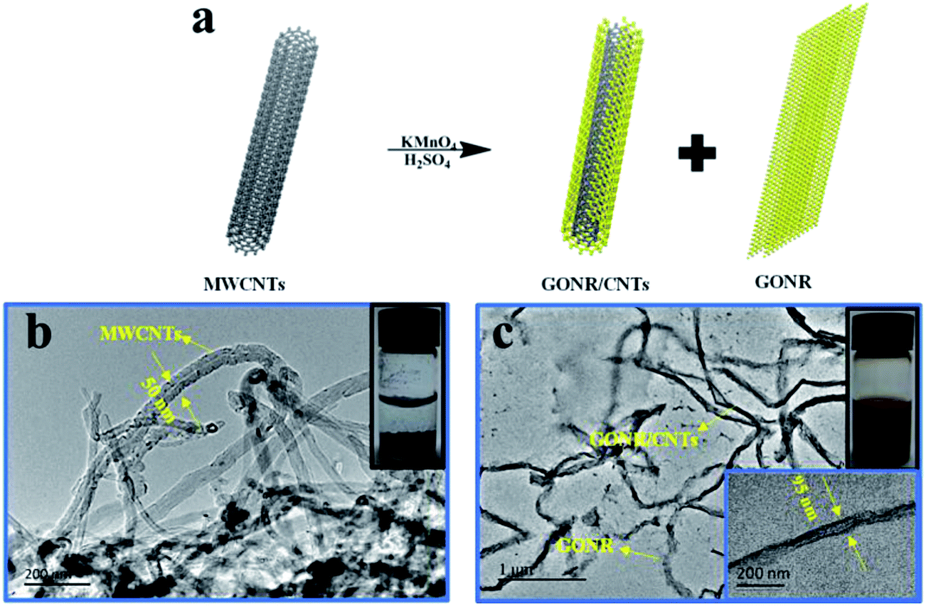
As shown in Fig. 1a, GONR/CNTs were synthesized from the oxidative unzipping of MWCNTs with KMnO4 as an oxidant in concentrated H2SO4 and H3PO4, similar to published procedures.29,30 The process transformed the insoluble pristine MWCNTs to hydroxyl and carboxyl38 functionalized GONR/CNTs that could be easily dispersed in water or other polar organic solvents (such as dimethylformamide). Fig. 1b shows a typical TEM image of tangled pristine MWCNTs with a diameter of 50 nm. After unzipping using KMnO4, the opened GONRs (Fig. 1c) look like ribbons with a much broader width than pristine MWCNTs (with an average width of 95 nm), indicating a successful unzipping of the MWCNTs. It should be noted that quite different from the GONRs unzipped from single-walled carbon nanotubes tending to form large amount of GO pieces,35 the ones prepared from MWCNTs are only longitudinally unzipped along the axial direction of the MWCNTs to develop well-defined nanoribbons containing carbon nanotubes with a continuous one-dimensional length for promoting charge transport.29 The nanoribbons were also verified from the SEM image of the GONRs (Fig. S1†). Moreover, from a comparison of the insets in Fig. 1b and c, the pristine MWCNTs tend to aggregate in water with much more precipitate on the bottom of the container, while the GONR/CNTs can be well dispersed in water and do not tangle together any more.
 |
| | Fig. 1 (a) The simplified synthesis process of the GONR/CNTs. (b) TEM image of pristine MWCNTs and (c) GONR/CNTs. The inset digital images show the pristine MWCNTs and GONR/CNTs dispersed in water, respectively. | |
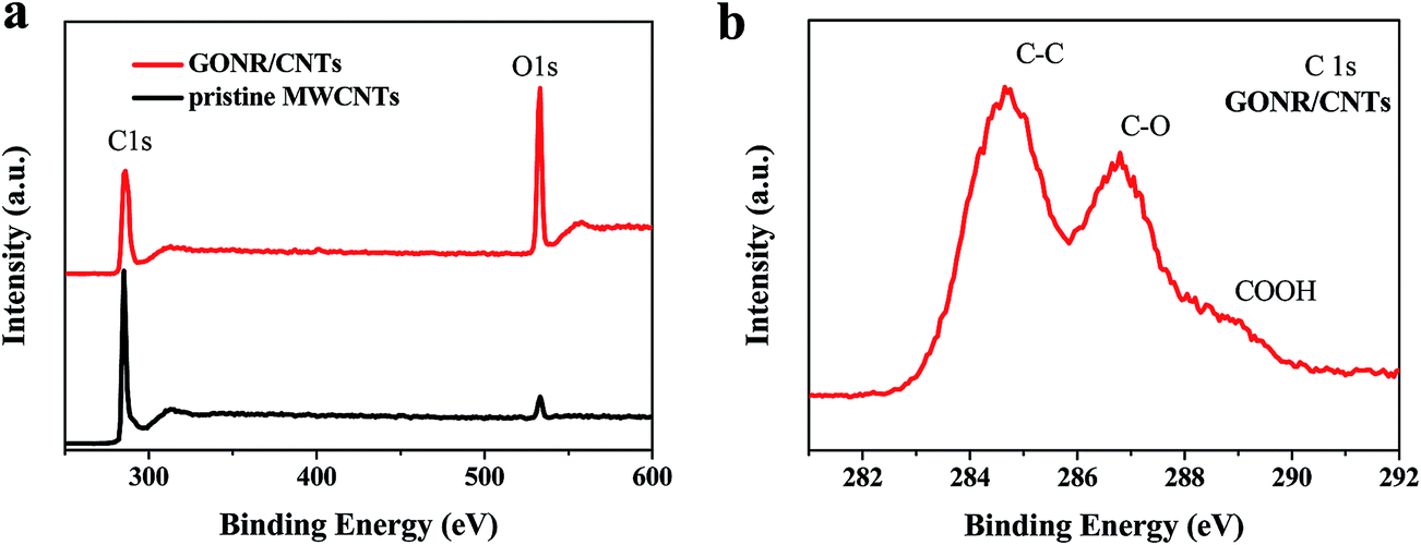
Due to the oxygen-containing functionalities such as carbonyls, carboxyls and hydroxyls that exist at the edge and on the surface of the GONR/CNTs, the degree of the oxidation of the GONR/CNTs was characterized using attenuated total reflectance infrared (ATR-IR) spectroscopy, thermogravimetric analysis (TGA) and X-ray photoelectron spectroscopy (XPS). Compared with the pristine MWCNTs, the ATR-IR spectroscopy (Fig. S2†) of the GONR/CNTs clearly reveals the appearance of the C![[double bond, length as m-dash]](https://www.rsc.org/images/entities/char_e001.gif) O stretch (∼1700 cm−1) and the COO–H/O–H stretch (∼3600–2800 cm−1), and the XPS C1s spectrum in Fig. 2 also presents the peaks of C–C, C–O and COOH in the GONR/CNTs structure. In addition, TGA shows the 7.9% and 48.3% weight loss of pristine MWCNTs and GONR/CNTs, respectively (Fig. S3†). The almost 50% weight loss implies the presence of carboxyl and hydroxyl functionalities in the GONR/CNTs. The degree of the oxidation of GONR/CNTs is also clearly evaluated from the corresponding XPS C1s and O1s spectrum (Fig. 2 and S4†),39 and a significant amount of oxygen is calculated to be 55.5 at%.
O stretch (∼1700 cm−1) and the COO–H/O–H stretch (∼3600–2800 cm−1), and the XPS C1s spectrum in Fig. 2 also presents the peaks of C–C, C–O and COOH in the GONR/CNTs structure. In addition, TGA shows the 7.9% and 48.3% weight loss of pristine MWCNTs and GONR/CNTs, respectively (Fig. S3†). The almost 50% weight loss implies the presence of carboxyl and hydroxyl functionalities in the GONR/CNTs. The degree of the oxidation of GONR/CNTs is also clearly evaluated from the corresponding XPS C1s and O1s spectrum (Fig. 2 and S4†),39 and a significant amount of oxygen is calculated to be 55.5 at%.
 |
| | Fig. 2 XPS characterization of carbon based materials. (a) XPS survey spectra of GONR/CNTs and pristine MWCNTs, (b) XPS carbon 1s spectrum of GONR/CNTs. | |
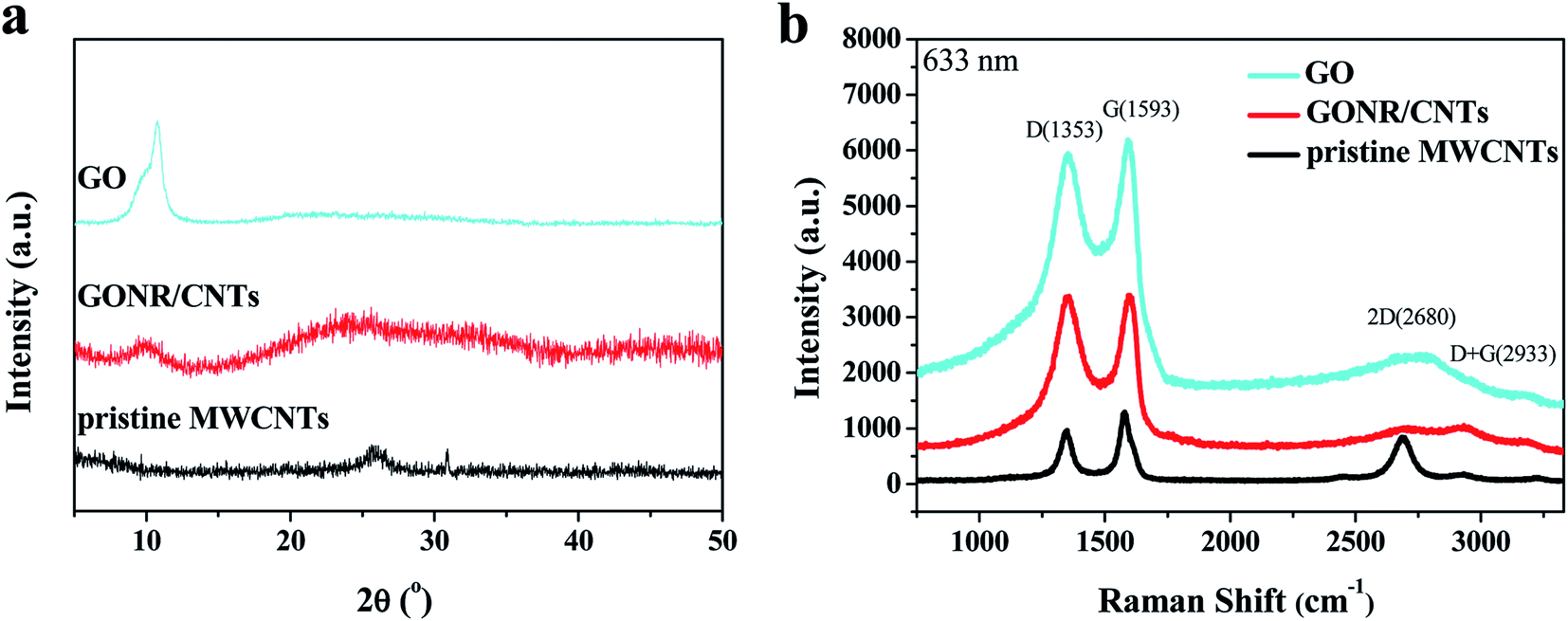
The successful partial unzipping of MWCNTs to GONR/CNTs can be further confirmed from XRD analysis and Raman spectra (Fig. 3). As shown in Fig. 3a, after being oxidized by KMnO4 and H2SO4, GONR/CNTs show a peak at ∼10.8° corresponding to the graphite (002) spacing, which does not exist for the MWCNTs. This peak is mainly assigned to the formation of hydroxyl and carboxyl groups at the edge of the GONR/CNTs, similar to that in graphene oxide. More importantly, the XRD pattern of the GONR/CNTs shows a diffuse peak at ∼25.8° whereas the MWCNTs show a sharp peak. This indicates that the GONR/CNTs unzipped from MWCNTs are regular and stacked. In addition, the MWCNTs before and after unzipping exhibit two characteristic peaks at 1353 and 1593 cm−1 in the Raman spectra (Fig. 3b), associated to the D and G peaks of the CNTs, respectively. Compared with the MWCNTs, the GONR/CNTs show a stronger D peak, due to the oxidation of the MWCNTs. The conversion of the MWCNTs to GONR/CNTs was also obviously evidenced by the variation in the 2D band at ∼2700 cm−1 from the sharp peak of the carbon nanotubes to the diffuse multi-peaks of the multi-nanoribbons.40
 |
| | Fig. 3 (a) X-ray diffraction of GO, GONR/CNTs and pristine MWCNTs. θ, diffraction angle; a.u., arbitrary units. (b) The Raman spectra of GO, GONR/CNTs and pristine MWCNTs at 633 nm. | |
3.2 The electrochemical and optical bandgap of GONR/CNTs
Since GONR/CNTs can be regarded as a quasi-one-dimensional polymer,35 the HOMO/LUMO energy levels of GONR/CNTs were measured using cyclic voltammetry (CV). It was performed in a three electrode cell using platinum electrodes at a scan rate of 50 mV s−1 and an Ag/Ag+ reference electrode in an anhydrous and nitrogen-saturated solution of 0.1 M tetrabutylammonium tetrafluoroborate (Bu4NBF4) in acetonitrile. Under these conditions, the onset oxidation potential (E1/2ox) of ferrocene was −0.02 V versus Ag/Ag+. The HOMO energy level of the polymer was determined from the oxidation onset of the second scan from the CV data. It was assumed that the redox potential of Fc/Fc+ has an absolute energy level of −4.40 eV relative to vacuum. The energies of the HOMO and LUMO levels were calculated according to the following equations:
| EHOMO = −(Φox + 4.4) (eV) |
| ELUMO = −(Φred + 4.4) (eV) |
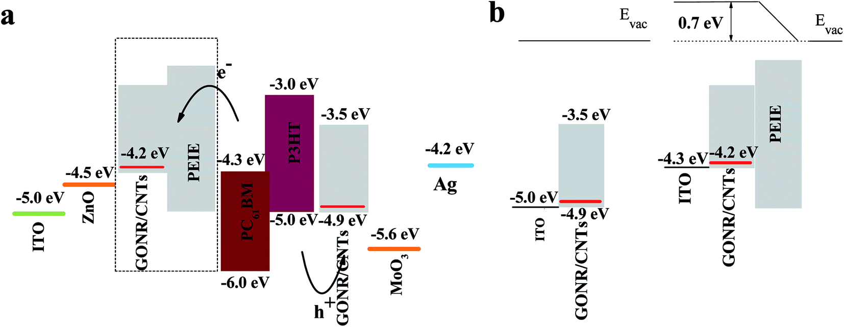
where Φox and Φred are the onset oxidation potential and the onset reduction potential versus Ag/Ag+, respectively.41,42 Introducing oxygen-rich groups around the GONR/CNTs has a significant effect on the bandgap of the resultant GONR/CNTs. As shown in Fig. 4a, from the values of Φox and Φred, the HOMO and LUMO energy levels for the GONR/CNTs are about −5.0 eV and −3.5 eV, respectively. The optical bandgap of the GONR/CNTs was further measured from the UV/Vis absorption spectrum. As shown in Fig. S5,† the absorption peak of the GONR/CNTs appears at 235 nm and an onset of the spectrum appears at around 800 nm with a 1.5 eV bandgap. The results are similar to the literature reported,35 which is also consistent with the electrochemical bandgap.
 |
| | Fig. 4 (a) Cyclic voltammetry of the GONR/CNTs drop-cast on a Pt electrode in a 0.1 mol L−1 Bu4NPF6–acetonitrile solution at a scan rate of 50 mV s−1. (b) Work function of bare ITO, GONR/CNT-coated-ITO and PEIE-coated-GONR/CNTs measured using the Kelvin probe method. | |
3.3 The electrical properties of GONR/CNTs
To compare the conductivity of the GONR/CNTs with pure GONRs, conductivity measurements were conducted using the structures ITO/GONR/CNTs/Au and ITO/GONR/Au. The fabrication process is described in the experimental section. Their J–V characteristics are shown in Fig. S6.† As shown, the J–V curves exhibit a linear relationship with the voltage applied. The conductivities of the films were estimated from the slopes of the curves. It is obvious that GONR/CNTs exhibit a better conductivity than pure GONRs.
To measure the electrical properties of the GONR/CNTs, the work function of the film was measured using the Kelvin probe method, and the surface work function is displayed in Fig. 4b. From the results, we can find that the GONR/CNT-coated-ITO film shows a relatively high work function of 4.9 eV (see Fig. 4b), which is equal to the HOMO levels of most polymer donors, such as P3HT (Fig. 5a), thus it is suitable for hole transporting.35 To further exploit the application of GONR/CNTs in cathode modification, an attempt was made to spin coat PEIE onto the GONR/CNTs to lower the work function. Delightfully, after being modified by a thin layer of PEIE (ca.10 nm), the work function of the GONR/CNTs was dramatically reduced to 4.2 eV (Fig. 4b) due to the neutral amine content in PEIE creating an interfacial dipole moment at the interface.36,43 It results in a vacuum level shift of about 0.7 eV, leading to a substantial change in the work function of the GONR/CNTs, as shown in Fig. 5b. The reduced work function is well matched, even better than ZnO (with a work function of 4.5 eV), with the LUMO levels of the fullerene acceptor, to make the GONR/CNTs act as an ETL in PSCs. From the energy level diagram of the device (Fig. 5a) we can discover that the GONR/CNTs employed as both a HTL and an ETL can construct a good energy level alignment in the device for charge extraction, transport and collection.
 |
| | Fig. 5 (a) Energy level diagram of the materials used in the inverted devices. (b) Illustration of the vacuum level shift and reduced work function of GONR/CNT-coated-ITO after deposition of the PEIE layer. | |
3.4 Photovoltaic performance and characterization
By employing GONR/CNTs as the interfacial layer, solar cell devices with the structure ITO/GONR/CNTs/PEIE/P3HT:PC61BM/GONR/CNTs/Ag were fabricated to determine the function of GONR/CNTs (Fig. 6). The molecular structures of P3HT, PC61BM and PEIE, and the device structure of modified GONR/CNTs and GONR/CNTs as interfacial layers are shown in Fig. 6a and b. The GONR/CNT layer was deposited by spin coating from its aqueous solution with a concentration of 3 mg mL−1 to give a thickness of about 2 nm. The J–V characteristics of the inverted polymer cells under AM 1.5G irradiation at 100 mW cm−2 are displayed in Fig. 7, and the electrical parameters are listed in Table 1. The performance data is averaged from 50 devices prepared on different days. Devices with ZnO as an ETL and MoO3 as a HTL were also prepared as control devices for comparison. As shown in Fig. 7 and Table 1, the control device shows a PCE of ∼3.1% with a reasonable Jsc of 8.75 mA cm−2, Voc of 0.60 V and an FF value of 58%, in good agreement with the literature.44 When the MoO3 HTL is replaced by a thin layer of GONR/CNTs, the device delivers a comparable efficiency of ∼3.0% to the control one, suggesting the effective anode modification by the GONR/CNTs. More intriguingly, through the incorporation of GONR/CNTs/PEIE as an ETL to replace ZnO, the device with the configuration ITO/GONR/CNTs/PEIE/P3HT:PC61BM/MoO3/Ag yields an all improved PCE of 3.7%, together with a Jsc of 9.16 mA cm−2, a Voc of 0.63 V and an FF value of 0.64 V. The distinct improvement in the PCE and corresponding parameters mainly results from the better energy alignment and the structure of the GONR/CNTs with a certain conductivity, as supported by the energy level diagram in Fig. 5.
 |
| | Fig. 6 (a) Structure of P3HT, PC61BM and PEIE. (b) Schematic illustration of the P3HT:PC61BM BHJ-based PSC device with GONR/CNTs as the HTL and ETL, and the inset shows the structure of the GONR/CNTs in the film. | |
 |
| | Fig. 7 (a) J–V characteristics of P3HT:PC61BM-based active layer inverted cells with various ETLs and HTLs under AM 1.5G irradiation at 100 mW cm−2. (b) Incident photo-to-electron conversion efficiency (IPCE) spectra of the inverted devices with the various ETLs and HTLs. | |
Table 1 Summary of the photovoltaic performance of inverted P3HT:PC61BM solar cells with various ETLs and HTLs
| Device structurea |
Jsc [mA cm−2] |
Voc [V] |
FF |
PCE [%] |
| All the devices of this work: all values represent averages from six 4 mm2 devices out of 50 devices prepared on different days with single chip measuring under AM 1.5 with 100 mW cm−2 irradiation. |
| ITO/ZnO/P3HT:PC61BM/MoO3/Ag |
8.75 ± 0.25 |
0.60 ± 0.01 |
0.58 ± 0.01 |
3.10 ± 0.07 |
| ITO/ZnO/P3HT:PC61BM/GONR/CNTs/Ag |
7.93 ± 0.22 |
0.61 ± 0.01 |
0.62 ± 0.01 |
3.00 ± 0.09 |
| ITO/GONR/CNTs/PEIE/P3HT:PC61BM/MoO3/Ag |
9.16 ± 0.22 |
0.63 ± 0.01 |
0.64 ± 0.01 |
3.70 ± 0.09 |
| ITO/GONR/CNTs/PEIE/P3HT:PC61BM/GONR/CNTs/Ag |
8.53 ± 0.24 |
0.63 ± 0.01 |
0.63 ± 0.01 |
3.42 ± 0.08 |
Moreover, the organic/organic interface between GONR/CNTs/PEIE and P3HT:PC61BM favors imitate contact and a much smoother morphology of P3HT:PC61BM, which is revealed in Fig. 8. In view of the effective function of the GONR/CNTs, the multifunctional nanoribbons are incorporated into the inverted devices as both a HTL and an ETL. As expected, the device with the GONR/CNT HTL and GONR/CNTs/PEIE ETL achieves a remarkably improved PCE of 3.42%, with a Jsc of 8.53 mA cm−2, Voc of 0.63 V, and an FF value of 63%. Fig. 7 shows the IPCEs corresponding to the J–V characteristics. The device with the GONR/CNT based ETL and HTL shows a calculated Jsc of 8.28 mA cm−2, which is consistent with the J–V characteristics. To investigate the universality of the interfacial layer, a PTB7:PC71BM-based active layer was used to fabricate devices with the structures ITO/ZnO/PTB7:PC71BM/MoO3/Ag and ITO/GONR/CNTs/PEIE/PTB7:PC71BM/GONR/CNTs/Ag. As shown in Fig. 9 and Table 2, the GONR/CNT interfacial layer also worked well in a PTB7:PC71BM-based active layer inverted solar cell. Compared with the ZnO and MoO3 interfacial layer, the devices with GONR/CNTs as the HTL and ETL achieved a remarkably improved PCE of 7.39%, with a Jsc of 14.65 mA cm−2, Voc of 0.73 V, and an FF value of 69%.
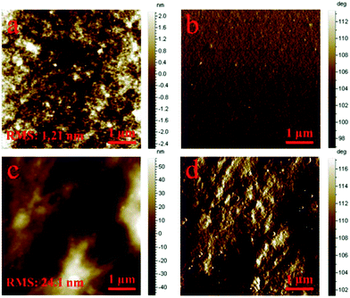 |
| | Fig. 8 AFM height and phase images of P3HT:PC61BM film on (a and b) ITO/GONR/CNTs/PEIE ETL and (c and d) an ITO/ZnO ETL, and (a and c) are the height images, (b and d) are the phase images. The scan size is 5 μm × 5 μm and the scan rate is 1 Hz for all of the images. | |
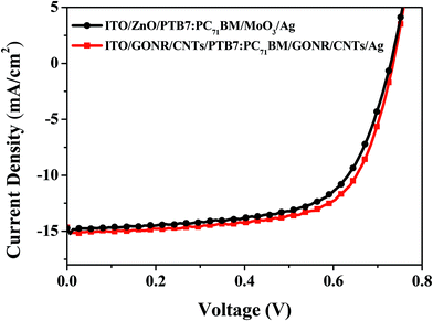 |
| | Fig. 9 J–V characteristics of PTB7:PC71BM-based active layer inverted cells with various cathode interfacial layers under AM 1.5 G irradiation at 100 mW cm−2. | |
Table 2 Summary of the photovoltaic performance of inverted PTB7:PC71BM-based solar cells with various ETLs and HTLs
| Device structurea |
Jsc [mA cm−2] |
Voc [V] |
FF |
PCEb [%] |
| Device configuration: glass/ITO/ETL/PTB7:PC71BM (1:1.5 w/w, 130–180 nm)/HTL/Ag (90 nm). All the PCE were averaged over 15 devices. |
| ITO/ZnO/PTB7:PC71BM/MoO3/Ag |
14.73 ± 0.57 |
0.73 ± 0.01 |
0.65 ± 0.02 |
6.97 ± 0.11 |
| ITO/GONR/CNTs/PEIE/PTB7:PC71BM/GONR/CNTs/Ag |
14.65 ± 0.45 |
0.73 ± 0.01 |
0.69 ± 0.03 |
7.39 ± 0.13 |
3.5 Evaluation of device stability
Stability is an important factor for commercial application, hence the degradation of the device without any encapsulation in air (relative humidity ca. 15%; temperature ca. 22 °C) was observed for 30 days. Fig. 10 shows the normalized efficiency of the inverted devices with the structures ITO/GONR/CNTs/PEIE/P3HT:PC61BM/GONR/CNTs/Ag and ITO/ZnO/P3HT:PC61BM/MoO3/Ag. Compared with ZnO and MoO3, the GONR/CNT interfacial layers ensure devices with improved long-term stability. The PCE of the GONR/CNT interfacial based layer device can be maintained at 85% of its initial efficiency after a storage time of 30 days, while the ZnO interfacial layer based device only retains 72% of its initial efficiency. We infer that the main reason for the stabilities of these devices is probably due to the morphology of the active layer. The morphology of the P3HT:PCBM layer on GONR/CNTs/PEIE exhibits a better surface with less roughness than that on ZnO. Therefore, GONR/CNTs should be a potential interface material for highly efficient and stable PSCs.
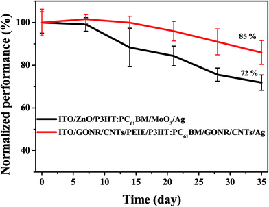 |
| | Fig. 10 Normalized PCE of inverted devices with the structures ITO/GONR/CNTs/PEIE/P3HT:PC61BM/GONR/CNTs/Ag and ITO/ZnO/P3HT:PC61BM/MoO3/Ag as a function of storage time in air without any encapsulation. | |
4. Conclusions
In conclusion, low cost and solution processible GONR/CNTs partially unzipped from MWCNTs were demonstrated. Unzipping of MWCNTs can endow GONR/CNTs with continuous nanoribbons. What’s more, GONR/CNTs have an open bandgap and the work function can easily be tuned by simple modification. As a result, with GONR/CNTs and PEIE modified GONR/CNTs as a HTL and an ETL, solution processed P3HT:PC61BM-based and PTB7:PC71BM-based PSCs achieved a high PCE of 3.42% and 7.39%, respectively. These results are even higher than the ZnO ETL and MoO3 HTL based device. Furthermore, the GONR/CNT interlayer also ensures a device with a significant high stability. Therefore, the multifunctional GONR/CNTs unzipped from MWCNTs would be promising interfacial materials for solution processed high performance PSCs. Moreover, after further reduction, such GONR/CNTs are also expected to have the potential for electrode applications due to their high conductivity.
Acknowledgements
This work was financially supported by the National Science Fund for Distinguished Young Scholars (51425304), National Natural Science Foundation of China (51273088, 51263016 and 51473075), and National Basic Research Program of China (973 Program 2014CB260409).
References
- N. S. Sariciftci, L. Smilowitz, A. J. Heeger and F. Wudl, Science, 1992, 258, 1474–1476 CAS.
- G. Li, V. Shrotriya, J. S. Huang, Y. Yao, T. Moriarty, K. Emery and Y. Yang, Nat. Mater., 2005, 4, 864–868 CrossRef CAS PubMed.
- G. Yu, J. Gao, J. C. Hummelen, F. Wudl and A. J. Heeger, Science, 1995, 270, 1789–1791 CAS.
- T. B. Yang, W. Z. Cai, D. H. Qin, E. G. Wang, L. F. Lan, X. Gong, J. B. Peng and Y. Cao, J. Phys. Chem. C, 2010, 114, 6849–6853 CAS.
- P. W. M. Blom, V. D. Mihailetchi, L. J. A. Koster and D. E. Markov, Adv. Mater., 2007, 19, 1551–1566 CrossRef CAS PubMed.
- http://www.nrel.gov/ncpv/images/efficiency_chart.jpg.
- K. D. G. I. Jayawardena, L. J. Rozanski, C. A. Mills, M. J. Beliatis, N. A. Nismy and S. R. P. Silva, Nanoscale, 2013, 5, 8411–8427 RSC.
- Y. Y. Liang, Z. Xu, J. B. Xia, S. T. Tsai, Y. Wu, G. Li, C. Ray and L. P. Yu, Adv. Mater., 2010, 22, E135–E138 CrossRef CAS PubMed.
- J. B. You, L. T. Dou, K. Yoshimura, T. Kato, K. Ohya, T. Moriarty, K. Emery, C. C. Chen, J. Gao, G. Li and Y. Yang, Nat. Commun., 2013, 4, 1446 CrossRef PubMed.
- H. L. Yip, S. K. Hau, N. S. Baek, H. Ma and A. K. Y. Jen, Adv. Mater., 2008, 20, 2376–2382 CrossRef CAS PubMed.
- J. Y. Kim, S. H. Kim, H. H. Lee, K. Lee, W. L. Ma, X. Gong and A. J. Heeger, Adv. Mater., 2006, 18, 572–576 CrossRef CAS PubMed.
- A. C. Arango, L. R. Johnson, V. N. Bliznyuk, Z. Schlesinger, S. A. Carter and H. H. Horhold, Adv. Mater., 2000, 12, 1689–1692 CrossRef CAS.
- M. S. White, D. C. Olson, S. E. Shaheen, N. Kopidakis and D. S. Ginley, Appl. Phys. Lett., 2006, 89, 143517 CrossRef PubMed.
- J. B. You, C. C. Chen, L. T. Dou, S. Murase, H. S. Duan, S. A. Hawks, T. Xu, H. J. Son, L. P. Yu, G. Li and Y. Yang, Adv. Mater., 2012, 24, 5267–5272 CrossRef CAS PubMed.
- H. Choi, J. S. Park, E. Jeong, G. H. Kim, B. R. Lee, S. O. Kim, M. H. Song, H. Y. Woo and J. Y. Kim, Adv. Mater., 2011, 23, 2759–2763 CrossRef CAS PubMed.
- Y. X. Zhu, X. F. Xu, L. J. Zhang, J. W. Chen and Y. Cao, Sol. Energy Mater. Sol. Cells, 2012, 97, 83–88 CrossRef CAS PubMed.
- T. B. Yang, M. Wang, C. H. Duan, X. W. Hu, L. Huang, J. B. Peng, F. Huang and X. Gong, Energy Environ. Sci., 2012, 5, 8208–8214 CAS.
- Q. L. Bao and K. P. Loh, ACS Nano, 2012, 6, 3677–3694 CrossRef CAS PubMed.
- D. S. Yu, Y. Yang, M. Durstock, J. B. Baek and L. M. Dai, ACS Nano, 2010, 4, 5633–5640 CrossRef CAS PubMed.
- K. P. Loh, Q. L. Bao, P. K. Ang and J. X. Yang, J. Mater. Chem., 2010, 20, 2277–2289 RSC.
- C. X. Guo, G. H. Guai and C. M. Li, Adv. Energy Mater., 2011, 1, 448–452 CrossRef CAS PubMed.
- P. H. Wobkenberg, G. Eda, D. S. Leem, J. C. de Mello, D. D. C. Bradley, M. Chhowalla and T. D. Anthopoulos, Adv. Mater., 2011, 23, 1558–1562 CrossRef CAS PubMed.
- E. Kymakis, K. Savva, M. M. Stylianakis, C. Fotakis and E. Stratakis, Adv. Funct. Mater., 2013, 23, 2742–2749 CrossRef CAS PubMed.
- G. Kakavelakis, D. Konios, E. Stratakis and E. Kymakis, Chem. Mater., 2014, 26, 5988–5993 CrossRef CAS.
- L. Zhang, J. J. Liang, Y. Huang, Y. F. Ma, Y. Wang and Y. S. Chen, Carbon, 2009, 47, 3365–3368 CrossRef CAS PubMed.
- F. Bonaccorso and Z. P. Sun, Opt. Mater. Express, 2014, 4, 63–78 CrossRef.
- Y. Gao, H.-L. Yip, S. K. Hau, K. M. O’Malley, N. C. Cho, H. Chen and A. K.-Y. Jen, Appl. Phys. Lett., 2010, 97, 203306 CrossRef PubMed.
- J. Liu, Y. Xue, Y. Gao, D. Yu, M. Durstock and L. Dai, Adv. Mater., 2012, 24, 2228–2233 CrossRef CAS PubMed.
- D. V. Kosynkin, A. L. Higginbotham, A. Sinitskii, J. R. Lomeda, A. Dimiev, B. K. Price and J. M. Tour, Nature, 2009, 458, 872–875 CrossRef CAS PubMed.
- A. L. Higginbotham, D. V. Kosynkin, A. Sinitskii, Z. Z. Sun and J. M. Tour, ACS Nano, 2010, 4, 2059–2069 CrossRef CAS PubMed.
- Y. W. Son, M. L. Cohen and S. G. Louie, Phys. Rev. Lett., 2006, 97, 216803 CrossRef.
- M. Y. Han, B. Ozyilmaz, Y. B. Zhang and P. Kim, Phys. Rev. Lett., 2007, 98, 206805 CrossRef.
- X. L. Li, X. R. Wang, L. Zhang, S. W. Lee and H. J. Dai, Science, 2008, 319, 1229–1232 CrossRef CAS PubMed.
- L. M. Xie, H. L. Wang, C. H. Jin, X. R. Wang, L. Y. Jiao, K. Suenaga and H. J. Dai, J. Am. Chem. Soc., 2011, 133, 10394–10397 CrossRef CAS PubMed.
- J. Liu, G. H. Kim, Y. H. Xue, J. Y. Kim, J. B. Baek, M. Durstock and L. M. Dai, Adv. Mater., 2014, 26, 786–790 CrossRef CAS PubMed.
- Y. H. Zhou, C. Fuentes-Hernandez, J. Shim, J. Meyer, A. J. Giordano, H. Li, P. Winget, T. Papadopoulos, H. Cheun, J. Kim, M. Fenoll, A. Dindar, W. Haske, E. Najafabadi, T. M. Khan, H. Sojoudi, S. Barlow, S. Graham, J. L. Bredas, S. R. Marder, A. Kahn and B. Kippelen, Science, 2012, 336, 327–332 CrossRef CAS PubMed.
- Y. M. Sun, J. H. Seo, C. J. Takacs, J. Seifter and A. J. Heeger, Adv. Mater., 2011, 23, 1679–1683 CrossRef CAS PubMed.
- D. Li, M. B. Muller, S. Gilje, R. B. Kaner and G. G. Wallace, Nat. Nanotechnol., 2008, 3, 101–105 CrossRef CAS PubMed.
- Y. W. Zhu, S. Murali, W. W. Cai, X. S. Li, J. W. Suk, J. R. Potts and R. S. Ruoff, Adv. Mater., 2010, 22, 5226 CrossRef CAS PubMed.
- A. C. Ferrari, J. C. Meyer, V. Scardaci, C. Casiraghi, M. Lazzeri, F. Mauri, S. Piscanec, D. Jiang, K. S. Novoselov, S. Roth and A. K. Geim, Phys. Rev. Lett., 2006, 97, 187401 CrossRef CAS.
- C. P. Chen, S. H. Chan, T. C. Chao, C. Ting and B. T. Ko, J. Am. Chem. Soc., 2008, 130, 12828–12833 CrossRef CAS PubMed.
- Q. D. Zheng, B. J. Jung, J. Sun and H. E. Katz, J. Am. Chem. Soc., 2010, 132, 5394–5404 CrossRef CAS PubMed.
- A. K. K. Kyaw, D. H. Wang, V. Gupta, J. Zhang, S. Chand, G. C. Bazan and A. J. Heeger, Adv. Mater., 2013, 25, 2397–2402 CrossRef CAS PubMed.
- M. T. Dang, L. Hirsch and G. Wantz, Adv. Mater., 2011, 23, 3597–3602 CrossRef CAS PubMed.
Footnote |
| † Electronic supplementary information (ESI) available: The detailed experimental sections and the corresponding characterization are in the ESI. See DOI: 10.1039/c5ra04657b |
|
| This journal is © The Royal Society of Chemistry 2015 |
Click here to see how this site uses Cookies. View our privacy policy here.