DOI:
10.1039/D5RA02550H
(Paper)
RSC Adv., 2025,
15, 17906-17932
Computational analysis of LiMgI3: a promising material for solar energy conversion†
Received
12th April 2025
, Accepted 22nd May 2025
First published on 29th May 2025
Abstract
This work employs density functional theory (DFT) using CASTEP to investigate the structural, electronic, and optical properties of cubic LiMgI3 as an absorber material. The lattice parameters we examined match quite well with earlier theoretical results, and the phonon dispersion confirmed its dynamic stability. The electronic band structure and density of states (DOS) revealed that LiMgI3 is a semiconductor, with band gaps of 1.162 eV using the GGA method and 1.922 eV using the HSE06 hybrid functional. Optical properties were evaluated within the photon energy range of 0–14 eV, key optical characteristics-such as absorption coefficient, reflectivity, refractive index, dielectric response, optical conductivity, and energy loss, all indicating excellent light-harvesting potential. To assess its device applicability, SCAPS-1D simulation software was used to model various solar cell architectures with LiMgI3 as the absorber. A total of 60 configurations combining different electron transport layers (ETLs) such as WS2, IGZO, TiO2, ZnO, ZnS, and PCBM, and hole transport layers (HTLs) like Cu2O, CuO, CBTS, CuI, P3HT, PEDOT:PSS, CuSCN, Spiro-OMeTAD, PTAA, and CdTe were evaluated. The ITO/WS2/LiMgI3/Cu2O/Ni structure yielded the best performance, with a power conversion efficiency (PCE) of 20.73%, open circuit voltage (VOC) of 1.495 V, a short circuit current (JSC) of 15.78 mA cm−2, and fill factor (FF) of 87.81%. This study analyzes how absorber and electron transport layer (ETL) thickness affect key photovoltaic parameters. It also examines the valence band offset (VBO) and conduction band offset (CBO) characteristics of different ETLs. The study further investigates the impact of series and shunt resistances, temperature, quantum efficiency (QE), capacitance–voltage (C–V) Characteristics, generation–recombination response, current density–voltage (J–V) characteristics, and impedance spectra on improving device performance. The exceptional photon capture efficiency of LiMgI3 perovskite solar cells (PVSKs) holds significant potential for advancing photovoltaic and optoelectronic device technologies.
1 Introduction
The growing global demand for energy, driven by population and economic expansion, has been predominantly supported by fossil fuel sources such as coal, petroleum, and natural gas.1,2 However, these non-renewable resources contribute significantly to CO2 emissions, posing serious environmental and sustainability concerns.3,4 In response, the progress in sustainable and clean energy technologies, particularly solar photovoltaics (PV), has gained critical importance in addressing climate change.5–9
Among the emerging PV technologies, perovskite solar cells (PSCs) have attracted considerable attention due to their remarkable rise in power conversion efficiency (PCE) from 3.8% in 2009 to over 25% in recent years.10,11 The halide perovskite absorber material is expressed by the formula ABX3, where A is a monovalent cation, B denotes a divalent metal, and X indicates a halide anion.12 These materials exhibit tunable bandgaps, high absorption rates, minimal exciton binding energies, and long carrier diffusion lengths, making them ideal candidates for high-efficiency solar cells.13–17 Hybrid organic–inorganic perovskites, especially those incorporating formamidinium (FA) or methylammonium (MA) cations, have demonstrated efficiencies above 20%.18 Their low-cost fabrication and solution-processable nature mark them as promising third-generation PV technologies.19 Despite their advantages, the sustained performance over time of organic–inorganic hybrid perovskite photovoltaic devices remains a significant challenge due to their susceptibility to degradation under chemical and thermal pressure.20 Furthermore, the toxicity of lead-based perovskites raises environmental and health concerns, hindering commercialization.21–25 Although lead-free photovoltaic cells generally have lower efficiency than their lead (Pb)-based counterparts, finding non-toxic alternatives is critical. As a result, elements like tin (Sn2+), germanium (Ge2+), antimony (Sb2+), and bismuth (Bi2+) are being used to substitute Pb in the B-site.18,26 However, magnesium (Mg) was selected over Sn2+, Ge2+, Sb2+, and Bi2+ due to its greater chemical stability, environmental safety, and promising optoelectronic properties.27 Sn2+ and Ge2+ are prone to oxidation, while Sb2+ and Bi2+ typically lead to indirect bandgaps and limited charge transport.28 In contrast, Mg offers a direct bandgap of 1.92 eV (Heyd–Scuseria–Ernzerhof) and a high absorption coefficient (>105 cm−1), positioning LiMgI3 as a promising lead-free perovskite absorber for stable and efficient solar cells.
The stability of perovskite materials has been enhanced through the addition of K and Rb atoms,29–32 especially in compounds like KGeX3 and RbGX3 (where X = Cl or Br). CsPbCl3, CsPbBr3, and CsPbI3 have gained significant interest for their excellent optoelectronic properties. CsPbCl3 has a large bandgap (>3.0 eV), making it unsuitable for photovoltaic applications.18,33–35 In contrast, CsPbBr3 offers a balanced 2.3 eV bandgap and superior phase stability, leading to improved device longevity and light absorption.36–38
The selection of electron transport layers (ETLs) and hole transport layers (HTLs) plays a crucial role in determining the efficiency and durability of perovskite solar cells (PSCs). The material properties of transport layers significantly influence the stability and performance of PSCs. When selecting an HTL for PSCs, it is crucial to consider material features such as cost, hole mobility, and valence band offset.39 Since the development of dye-sensitized solar cells (DSSCs), TiO2 has been valued as an important ETL material because of its extensive bandgap and chemical stability.40–44 In contrast, polymer-based hole transport layers like Spiro-MeOTAD and P3HT45 provide thermal and moisture resistance, enhancing device longevity.46 Recently, copper barium thiocyanate (CBTS) has emerged as a promising inorganic HTL due to its stability, non-toxic nature, and tunable bandgap.47,48 A maximum PCE of 28.4% is recorded in PSCs using TiO2 as the ETL and MASnI3 as the absorbing layer.49 According to recent research, CsPbI3-based devices with CBTS as HTL achieved PCE values of 16.71%, 17.90%, 17.86%, 14.47%, 17.76%, and 17.82% when using PCBM, TiO2, ZnO, C60, IGZO, and WS2 as ETLs, respectively.50,51 In their experimental study, Song et al.52 found that CsSnI3 had a PCE of 2.02%. Conversely, Adnan et al.,53 through theoretical analysis, improved the PCE to 15.83%. Based on our analysis, LiMgI3, the absorber material, is non-toxic and therefore a better option for our society. On the other hand, density functional theory (DFT) is widely used to study the optical and electrical properties of halide perovskites for photovoltaic applications.54–56 Experimental and theoretical investigations conducted in recent times have provided fresh perspectives on the structure of CsSnCl3.57–59 To evaluate LiMgI3's potential as an absorber material for solar cells, an extensive examination of its structural, optical, and electrical features will be performed.
The objective of this research is to assess the structural, electronic, and optical properties of the LiMgI3 absorber, employing first-principles methods within the DFT framework, and using CASTEP software. We calculated the lattice parameters and unit cell volumes of the LiMgI3 compound using both the hybrid HSE06 (Heyd–Scuseria–Ernzerhof) and generalized gradient approximation (GGA) methods. The bandgap (Eg) values from GGA and HSE06 confirm the semiconducting nature without bands crossing the Fermi level. Additionally, we analyzed crucial optical properties such as absorption, reflectivity, refractive index, dielectric function, conductivity, and loss function. We aimed to identify the optimal combinations of WS2, IGZO, TiO2, ZnO, ZnS, PCBM as ETLs, along with Cu2O, CuO, CBTS, CuI, P3HT, PEDOT:PSS, CuSCN, Spiro-OMeTAD, PTAA and CdTe as HTLs, paired with the LiMgI3 absorber, for optimizing device performance via SCAPS-1D simulation techniques. In our current study, we investigated various thicknesses and defect densities for the absorber, ETL, and HTL layers. Furthermore, we evaluated the series and shunt resistance, current–voltage (J–V) characteristics, capacitance–voltage (C–V) responses, quantum efficiency (QE), impedance study, generation and recombination rates, and valence and conduction band offsets across different ETLs to gain further insights into the solar cell architectures studied.
2 Materials used and methodology
2.1 DFT-based first-principles study of LiMgI3 absorber
This research utilizes density functional theory (DFT) with the Cambridge Serial Total Energy Package (CASTEP) framework to analyze the structural, optical, and electronic features of the alkali halide perovskite LiMgI3.60–62 This approach utilizes the generalized gradient approximation (GGA) for the exchange-correlation potential, specifically using the Perdew–Burke–Ernzerhof (PBE) parameter.60,63 For precise determination of the electronic band gaps of the subject compound, the HSE06 hybrid functional (Heyd–Scuseria–Ernzerhof) is utilized.62 Additionally, to simulate the interactions between valence electrons and ionic cores, the Vanderbilt-type ultrasoft pseudopotential method was employed.64 Elastic constants were derived using the linear finite strain–stress approach, implemented within the CASTEP code.65 The atomic calculations utilized the electronic configurations of Li – 1s, 2s, 3p Mg – 2s, 2p, 3s and I – 4d, 5s, 5p. To find the lowest energy state of the stable structure, the Broyden–Fletcher–Goldfarb–Shanno (BFGS)66 algorithm was applied. To sample k-points in the first Brillouin zone (BZ), the Monkhorst–Pack grid method67 was applied to expand the plane-wave basis set, using a cutoff energy of 400 eV for GGA and 800 eV for HSE06. Accurate reciprocal space sampling was achieved by integrating the Brillouin zone using a 6 × 6 × 6 k-point mesh for GGA and a 2 × 2 × 2 mesh for HSE06, based on the Monkhorst–Pack method. The convergence criteria are defined as 5 × 10⁻⁶ eV per atom for total energy, 5 × 10⁻⁴ Å for maximum displacement, 0.03 eV Å−1 for maximum force, 0.001 Å for the maximum displacement, and 0.05 GPa for maximum stress. The cutoff energy (eV) vs. final energy (eV) for LiMgI3, and number of K-points vs. final energy (eV) for LiMgI3 was illustrated in Fig. S2 and S3.†
2.2 Numerical modeling using SCAPS-1D
This computational approach helps clarify the core principles of solar cells while focusing on the main parameters that impact their performance. Fig. 1 displays the SCAPS-1D simulation process. SCAPS-1D software employs numerical techniques to solve critical one-dimensional semiconductor equations.68–71 Poisson's equation (eqn (1))72 relates the distribution of charges to the electrostatic potential, as illustrated in eqn (1).| |
 | (1) |
in the above equation, the relative permittivity is denoted by εr, ε0 indicates the permittivity of free space, ND and NA represent the ionized donor and acceptor densities, ρp and ρn stand for the electron and hole distributions, n and p represent electron and hole densities, q represents the electronic charge, and ψ signifies the electronic potential. The continuity equation, which simultaneously analyses recombination, generation, drift, and diffusion processes, is regarded as the fundamental governing equation. Eqn (2) and (3) provide the respective formulations for changes in electron and hole concentrations| |
 | (2) |
| |
 | (3) |
Here, the current densities of electrons and holes are represented by Jn and Jp; Gn and Gp for electron and hole generation; and Rn and Rp refer to electron and hole recombination rates. The charge carrier drift-diffusion equations, provided in eqn (4) and (5) below, are employed to determine the electron and hole current densities in solar cells.in the above equation, μn and μp indicate the mobilities of carriers, while Dn and Dp are the diffusion coefficients for electrons and holes, respectively. According to the Einstein relationship, the carrier's mobility and lifetime both affect the diffusion coefficient.73 Moreover, the newly adapted Eg-sqrt model, which is a variant of the conventional sqrt (hv − Eg) model, was utilized to obtain the absorption constant for films. This relationship is expressed through the “Tauc laws” and can be seen in eqn (6).| |
 | (6) |
Here, α denotes the absorption coefficient, Eg represents the bandgap, and hv indicates the photon energy. The model constants α0 and β0 are related to the traditional constants A and B through eqn (7) and (8) as shown below| |
 | (7) |
| |
 | (8) |
 |
| | Fig. 1 The simulation procedure applied in SCAPS-1D. | |
2.3 LiMgI3-based PSC structure
Fig. 2a shows the optimized solar cell's schematic construction. The single halide perovskite solar cell is structured by associating the LiMgI3 absorber layer with the ETL, HTL, front and back contact. Throughout the investigation, we used a branch of ETL (WS2, IGZO, TiO2, ZnO, ZnS, and PCBM) and HTL (Cu2O, CuO, CBTS, CuI, P3HT, PEDOT:PSS, CuSCN, Spiro-OMeTAD, PTAA, and CdTe) to identify the best-performing device. The ITO/WS2/LiMgI3/Cu2O/Ni configuration was identified as the most computationally efficient solar cell among these numerous configurations. LiMgI3 halide perovskite provides the ability to absorb light. It is confirmed by the investigation that the doped ETL and HTL form ohmic contacts, which efficiently confine photons and charge on both surfaces. The simulation's input parameters for the ITO, absorber layer, and ETLs are shown in Table 1, with the parameters for all HTLs found in Table 2. The input parameters for the interfacial defect layers are also provided in Table 3. All simulations have employed the AM 1.5 G sun spectrum, which has a power density of 1000 W m−2 at 300 K and a frequency of 1 MHz.
 |
| | Fig. 2 (a) The design configuration of the LiMgI3-based PSC. (b) Energy band alignment between the different ETL and HTL materials of LiMgI3 absorber. | |
Table 1 Input parameters of ITO,74 ETLs,50,74,76 absorber layers (LiMgI3)
| Parameters |
ITO |
WS2 |
TiO2 |
IGZO |
ZnO |
ZnS |
PCBM |
LiMgI3 |
| Thickness (nm) |
500 |
100 |
30 |
30 |
50 |
75 |
50 |
1000 |
| Bandgap, Eg (eV) |
3.5 |
1.8 |
3.2 |
3.05 |
3.3 |
2.80 |
2 |
1.92 |
| EA (eV) |
4 |
3.95 |
4 |
4.16 |
4 |
3.80 |
3.9 |
3.92 |
| εr |
9 |
13.6 |
9 |
10 |
9 |
9.00 |
3.9 |
6.96 |
| NC (cm−3) |
2.2 × 10¹⁸ |
1 × 10¹⁸ |
2 × 10¹⁸ |
5 × 10¹⁸ |
3.7 × 10¹⁸ |
2.2 × 10¹⁸ |
2.5 × 10²¹ |
6.26 × 10¹⁷ |
| NV (cm−3) |
1.8 × 10¹⁹ |
2.4 × 10¹⁹ |
1.8 × 10¹⁹ |
5 × 10¹⁸ |
1.8 × 10¹⁹ |
1.8 × 10¹⁹ |
2.5 × 10²¹ |
1.46 × 10¹⁸ |
| μn (cm2 V−1 s−1) |
20 |
100 |
20 |
15 |
100 |
100 |
0.2 |
446 |
| μh (cm2 V−1 s−1) |
10 |
100 |
10 |
0.1 |
25 |
25 |
0.2 |
54.7 |
| ND (cm−3) |
1 × 10²¹ |
1 × 10¹⁸ |
9 × 10¹⁶ |
1 × 10¹⁷ |
1 × 10¹⁸ |
1 × 10¹⁹ |
2.9 × 10¹⁷ |
1 × 10⁹ |
| NA (cm−3) |
0 |
0 |
0 |
0 |
0 |
1 × 10⁶ |
0 |
0 |
| Nt (cm−3) |
1 × 10¹⁵ |
1 × 10¹⁵ |
1 × 10¹⁵ |
1 × 10¹⁵ |
1 × 10¹⁵ |
1 × 10¹⁵ |
1 × 10¹⁵ |
1 × 10¹⁵ |
Table 2 Input parameters of different HTLs50,74,77
| Parameters |
Cu2O |
CuO |
CBTS |
CuI |
P3HT |
PEDOT:PSS |
CuSCN |
Spiro-OMeTAD |
PTAA |
CdTe |
| Thickness (nm) |
50 |
50 |
100 |
100 |
50 |
50 |
50 |
200 |
150 |
200 |
| Bandgap, Eg (eV) |
2.2 |
1.51 |
1.9 |
3.1 |
1.7 |
1.6 |
3.6 |
3 |
2.96 |
1.5 |
| EA (eV) |
3.4 |
4.07 |
3.6 |
2.1 |
3.5 |
3.4 |
1.7 |
2.2 |
2.3 |
3.9 |
| εr |
7.5 |
18.1 |
5.4 |
6.5 |
3 |
3 |
10 |
3 |
9 |
9.4 |
| NC (cm−3) |
2 × 10¹⁹ |
2.2 × 10¹⁹ |
2.2 × 10¹⁸ |
2.2 × 10¹⁹ |
2 × 10²¹ |
2.2 × 10¹⁸ |
2.2 × 10¹⁹ |
2.2 × 10¹⁸ |
2 × 10²¹ |
8 × 10¹⁷ |
| NV (cm−3) |
1 × 10¹⁹ |
5.5 × 10²⁰ |
1.8 × 10¹⁹ |
1 × 10¹⁹ |
2 × 10²¹ |
1.8 × 10¹⁹ |
1.8 × 10¹⁸ |
1.8 × 10¹⁹ |
2 × 10²¹ |
1.8 × 10¹⁹ |
| μn (cm2 V−1 s−1) |
200 |
100 |
30 |
100 |
1.8 × 10⁻³ |
4.5 × 10⁻² |
100 |
2.1 × 10⁻³ |
1 |
3.2 × 10² |
| μh (cm2 V−1 s−1) |
8600 |
0.1 |
10 |
43.9 |
1.86 × 10⁻² |
4.5 × 10⁻² |
25 |
2.16 × 10⁻³ |
40 |
4 × 101 |
| ND (cm−3) |
0 |
0 |
0 |
0 |
0 |
0 |
0 |
0 |
0 |
0 |
| NA (cm−3) |
1 × 10¹⁸ |
1 × 10¹⁵ |
1 × 10¹⁸ |
1 × 10¹⁸ |
1 × 10¹⁸ |
1 × 10¹⁸ |
1 × 10¹⁸ |
1 × 10¹⁸ |
1 × 10¹⁸ |
2 × 10¹⁴ |
| Nt (cm−3) |
1 × 10¹⁵ |
1 × 10¹⁵ |
1 × 10¹⁵ |
1 × 10¹⁵ |
1 × 10¹⁵ |
1 × 10¹⁵ |
1 × 10¹⁵ |
1 × 10¹⁵ |
1 × 10¹⁵ |
1 × 10¹⁵ |
Table 3 Interface parameters used in this perovskite solar cell50
| Interface |
Defect type |
Capture cross section: electrons/holes (cm2) |
Energetic distribution |
Reference for defect energy levels, Et |
Interface defect density (cm−2) |
| ETL/LiMgI3 |
Neutral |
1 × 10⁻¹⁷ |
Single |
Above the VB maximum |
1 × 10¹⁰ |
| 1 × 10⁻¹⁸ |
| LiMgI3/Cu2O |
Neutral |
1 × 10⁻¹⁸ |
Single |
Above the VB maximum |
1 × 10¹⁰ |
| 1 × 10⁻¹⁹ |
2.4 The energy band structure of the LiMgI3 absorber with various ETLs and HTLs
Fig. 2b illustrates various solar cell configurations, each utilizing distinct types of ETL, HTL, absorbers, and front and back contacts. We conducted an in-depth analysis of six ETLs and ten HTLs, exploring 60 possible combinations in the ITO/ETL/LiMgI3/HTL/Ni configuration to determine the best theoretical pairing for the LiMgI3 absorber layer, as shown in Fig. 2b. According to Fig. 2b, our study found that WS2, featuring an energy gap of 1.8 eV, delivered the best results as an ETL in combination with Cu2O HTLs for single halide LiMgI3 devices. The front electrode, positioned at the incident plane of light, demands both high transmittance and excellent electrical conductivity. One of the most common materials for front electrodes is indium-tin-oxide (ITO), a type of transparent conductive oxide (TCO). Previous studies have indicated that the surface work function (WF) of ITO is approximately 3.5 eV.74 The selection of TCO materials in LiMgI3 PSCs is usually made by considering the device structure, band-gap compatibility, and the temperature needed for device fabrication. The back electrode is typically composed of metal materials like Ni. A high-quality back electrode can improve carrier collection and boost both the stability and efficiency of the device.75 Due to the mesoporous or planar structure adopted by most LiMgI3 PSCs, the Au electrode (WF ∼ 5.1 eV) is the most suitable, as depicted in Fig. 2b.
3 Result and discussion
3.1 DFT result analysis
3.1.1 Structural properties and dynamical stability. The LiMgI3 alkali-based single halide perovskite compounds take on a cubic ABM3 structure that corresponds to the Pm![[3 with combining macron]](https://www.rsc.org/images/entities/char_0033_0304.gif) m crystallographic space group (no. 221). The standard structural arrangement of this LiMgI3 material is demonstrated in Fig. 3a. This material's unit cells are made up of a formula unit with five atoms. The lattice parameters and unit cell volumes for the LiMgI3 compound are calculated using both the hybrid HSE06 (Heyd–Scuseria–Ernzerhof) and the generalized gradient approximation (GGA) methods. The GGA (HSE06) technique yields a lattice parameter of 5.805 (5.483) Å for LiMgI3 and a unit cell volume of 195.617 (164.850) Å3. LiMgI3 demonstrates the highest stability and ideal structure when the Li atom is located at the 1a Wyckoff position (0, 0, 0), the Mg atom is positioned at the 1b Wyckoff position (1/2, 1/2, 1/2), and the I atom is located at the 3c Wyckoff position (1/2, 0, 1/2). For this compound, all lattice parameters were relaxed throughout the geometry optimization procedure. This calculation indicates that the lattice parameters and unit cell volume of LiMgI3 are consistent with earlier theoretical findings,78 confirming the accuracy of our current results.
m crystallographic space group (no. 221). The standard structural arrangement of this LiMgI3 material is demonstrated in Fig. 3a. This material's unit cells are made up of a formula unit with five atoms. The lattice parameters and unit cell volumes for the LiMgI3 compound are calculated using both the hybrid HSE06 (Heyd–Scuseria–Ernzerhof) and the generalized gradient approximation (GGA) methods. The GGA (HSE06) technique yields a lattice parameter of 5.805 (5.483) Å for LiMgI3 and a unit cell volume of 195.617 (164.850) Å3. LiMgI3 demonstrates the highest stability and ideal structure when the Li atom is located at the 1a Wyckoff position (0, 0, 0), the Mg atom is positioned at the 1b Wyckoff position (1/2, 1/2, 1/2), and the I atom is located at the 3c Wyckoff position (1/2, 0, 1/2). For this compound, all lattice parameters were relaxed throughout the geometry optimization procedure. This calculation indicates that the lattice parameters and unit cell volume of LiMgI3 are consistent with earlier theoretical findings,78 confirming the accuracy of our current results.
 |
| | Fig. 3 (a) Crystal structure of LiMgI3 material (b) phonon dispersion plot of LiMgI3. | |
A material's dynamic stability is an important consideration when considering its feasibility for practical applications involving time-dependent external influences. Fig. 3b depicts the phonon dispersion curve (PDC), which is important in determining a material's dynamic stability. We computed the phonon dispersion curves at the high-symmetry locations (W–L–Γ–X–W–K) inside the Brillouin zone (BZ) to assess the dynamic stability of LiMgI3. Dynamically stable crystalline materials are characterized by the absence of imaginary frequencies inside the Brillouin zone.79 In contrast, the existence of an imaginary component suggests the occurrence of dynamic instability.80 The phonon dispersion curve (PDC) of LiMgI3 do not display any negative frequencies, indicating that this compound is dynamically stable. Nine optical modes and three acoustic modes are created by this stability, with the acoustic modes being zero at the Γ-point, as shown in Fig. 3b.
3.1.2 Electronic properties and of LiMgI3.
3.1.2.1 Electronic band structure. The electronic band structure plays an integral part in comprehending material properties such as conductivity81 and band gap, which are essential for the development of electronic and optoelectronic devices. The band structures of the investigated compound are presented in Fig. 4a and b using the GGA and HSE06 techniques, respectively. Both local functionals (GGA) and nonlocal functionals (HSE06) have been used to produce an accurate band gap and electronic band structure (EBS) prediction. However, the hybrid function (HSE06) is a more dependable method than GGA.77 The band spectrum is computed along directions of high symmetry (X–R–M–Γ–R) inside the Brillouin zone and it covers an energy spectrum from −6 to +8 eV. In both diagrams, a red dotted line placed at 0 eV represents the Fermi level (EF). Energy levels above the Fermi level (EF) indicate conduction bands, whereas energy levels below the Fermi level (EF) indicate valence bands. A direct band gap is the result of the conduction band minimum (CBM) and valence band maximum (VBM) being located at the same high symmetry point, while an indirect band gap is the result of their being located at separate high symmetry points.82 In both methods, the material obviously has an indirect band gap as the valence band maximum and conduction band minimum are detected at separate high-symmetry sites in the HSE06 and GGA functionals. The band gap values calculated using GGA (HSE06) are 1.162 (1.922) eV. For both the HSE06 and GGA functionals, the bands do not interact with each other or cross the Fermi level, suggesting a semiconducting nature.
 |
| | Fig. 4 Electronic band structure (a) GGA, (b) HSE06 of LiMgI3, and total and partial density of states (c) GGA, (d) HSE06 of LiMgI3. | |
| |
 | (9) |
Here, the value of ℏ is![[thin space (1/6-em)]](https://www.rsc.org/images/entities/char_2009.gif) 1.05 × 10⁻³⁴. The values of d2E/dk2 are derived from the E–K dispersion curve by fitting parabolic curves at symmetry points. Using eqn (1), we computed the effective hole mass
1.05 × 10⁻³⁴. The values of d2E/dk2 are derived from the E–K dispersion curve by fitting parabolic curves at symmetry points. Using eqn (1), we computed the effective hole mass  and electron mass
  as 0.321m0 and 0.0393m0, respectively. This material is most likely p-type since it has a higher effective hole mass
  than electron mass
  Reduced effective mass facilitates carrier transport, making it ideal for solar materials.84 The following formula uses the effective masses to determine the mobility (μe for electrons and μh for holes).85
| |
 | (10) |
Here, μ symbolizes mobility, and τ represents the carrier's relaxation duration. For iodide PVSK materials, a constant relaxation time of 10−14 seconds is advised according to the literature.86 The mobility of electrons and holes in LiMgI3 was measured at 446 and 54.7 cm2 V−1 s−1, respectively. We computed other electronic characteristics by applying the effective mass, such as the effective NC and NV at 300 K using the following formulas.87| |
 | (11) |
| |
 | (12) |
3.1.3 Optical properties. The effectiveness of a material in capturing and converting solar energy is largely determined by its optical properties, which describe its ability to absorb and manage light. The optical property of a material generally describes its behavior when exposed to electromagnetic radiation, especially in the visible light spectrum.88 The optical properties of LiMgI3, including absorption coefficient, reflectivity, refractive index, dielectric function, conductivity, and loss function, are analyzed using photon energy in the 0–14 eV range through both GGA and HSE06 methods. In Fig. 5, the optical properties of LiMgI3 are depicted for both the GGA and HSE06 methods.
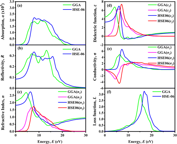 |
| | Fig. 5 Optical properties: (a) absorption, (b) reflectivity, (c) refractive index, (d) dielectric function, (e) conductivity and (f) loss function for LiMgI3. | |
The absorption coefficient of a material, which indicates how much light at a particular wavelength would reach the material before absorption and is used to determine the solar energy conversion efficiency, yields the quantity of absorption per optical medium unit length illustrated in Fig. 5a. The absorption spectra for LiMgI3, as calculated by both GGA and HSE06 methods, start from a non-zero energy level, signifying the existence of a band gap due to its semiconducting properties. The HSE06 approach displays a beginning point close to 5 eV, whereas the GGA method's absorption spectra for LiMgI3 start at around 2 eV. For the HSE06 method, the absorption peak value is approximately 2.25 at an energy of 8 eV. Conversely, for the GGA method, the peak absorption value is approximately 2 at 6.8 eV. The HSE06 method shows slightly higher absorption compared to the GGA method. The high absorption capacity of this material makes it a prime choice for solar cell applications.
Reflectivity is assessed by measuring how much light a compound reflects when it is subjected to light. Reflectivity is determined by the ratio of the incident wave's energy to the energy of the wave reflected from the surface.89 The reflectivity spectra of LiMgI3, plotted against photon energy, are presented in Fig. 5b using the HSE06 and GGA methods. The starting points of the reflectivity spectra differ between the GGA and HSE06 methods. The peak reflectivity value is 0.35 at 13.3 eV for the GGA method and 0.335 at 8 eV for the HSE06 method. It is noteworthy that the reflectivity spectra show a downward trend in the UV region.
The refractive index is a dimensionless value that numerically describes how light or radiation moves through a medium.90 The real and imaginary components of the refractive index for LiMgI3 are shown in Fig. 5c. The real part of the refractive index begins at 2.1 for the GGA method and 1.8 for the HSE06 method. Each method shows almost identical peak values, with 2.75 for HSE06 and 2.7 for GGA. The refractive index decreases significantly in the ultraviolet part of the spectrum for both methods.
The dielectric function is a key parameter related to the rate of charge carrier recombination in a material.91 The real and imaginary components of the dielectric function are illustrated in Fig. 5d. The complex dielectric function, represented by ε1 + ε2, combines the real (ε1) and imaginary (ε2) parts. The real part begins at 4.5 for the GGA functional and at 3.3 for the HSE06 functional when measured at 0 eV. The peak values for GGA and HSE06 are 7 at 6.2 eV and 6.8 at 4.3 eV, respectively, which are nearly identical.
Optical conductivity measures how well a material conducts electric current in response to an electromagnetic field. It quantifies the interaction between light and the material, indicating how the material absorbs or reflects light. The optical conductivity of LiMgI3 is depicted in Fig. 5e. The peak real part conductivity for LiMgI3 is 6.66 with HSE06 and 4.9 with GGA, showing greater conductivity for the HSE06 method. In contrast, the imaginary part decreases steadily in both infrared and visible regions.
The loss function (L) is crucial for understanding how energy is lost through heating, scattering, or dispersion as light moves through a material.92,93 Fig. 5f provides an illustration of the loss function spectra for LiMgI3. The drop in the loss function at lower energies is associated with the increased absorption in that specific area. The energy equivalent of the largest peak in the loss function is plasma frequency.94 The plasma frequency of LiMgI3 differs between the GGA and HSE06 methods, with the peak of the loss function appearing at distinct energy points. The peak value of the loss function is 3.25 for the HSE06 method at 17 eV and 3 for the GGA method at 15.45 eV.
3.1.4 Thermo-mechanical properties of LiMgI3. The mechanical and thermal parameters presented in Table S1† were derived using the established formulas reported for A2BIrCl6 (A = Cs, Rb; B = Na, K)95 and ANiX (A = Sc, Ti, Y, Zr, Hf; X = Bi, Sn)81 in previously published literature. The mechanical and thermal characteristics of LiMgI3 reveal a material with relatively soft and ductile behavior, suggesting its potential suitability for flexible and low-temperature device applications.96 To evaluate the stability of the composites, it is essential to consider the Born–Huang stability criterion,97,98 which is expressed as follows:| | |
C11 + 2C12 > 0 (spinodal criteria),
| (13) |
| | |
C11 − C12 > 0 (Born criteria),
| (14) |
| | |
C44 > 0 (shear criteria)
| (15) |
Table S3† demonstrates that the elastic constants C11, C12, and C44 for LiMgI3 fulfill the mechanical stability requirements. The elastic constant tends as follows: C11 < C12 < C44. The computed bulk modulus B (15.50 GPa) and shear modulus G (6.84 GPa) are relatively low, implying that the material is compressible and less resistant to shape deformation. The Young's modulus Y of 17.89 GPa supports this observation, confirming the soft nature of the crystal. Poisson's ratio (ν) serves as an indicator of whether a material behaves in a brittle or ductile manner. Values under 0.26 typically point to brittleness and covalent bonding, whereas those over 0.26 imply ductility and ionic bonding. Based on the data presented in Table S3,† it can be inferred that the materials LiMgI3 (≈0.30) demonstrate ductile behavior and are characterized by ionic bonding, as their Poisson's ratio values are above 0.26. On the other hand, Pugh's ratio (B/G = 2.27) exceeding the critical threshold of 1.75, LiMgI3 demonstrates ductile characteristics and possess ionic bond. Thermal analysis shows that the compound has a relatively low density of 4.14 g cm−3, and modest sound velocities (longitudinal (Vl),: 2.43 km s−1, transverse Vt: 1.28 km s−1) leading to an average sound velocity (νm) of 1.43 km s−1. The Debye temperature (θD) is a key parameter that reflects several material properties, particularly thermal conductivity and elastic nature. A high Debye temperature typically signifies that a material is stiff, strongly bonded, and supports fast sound wave propagation.99 The Debye temperature (θD), calculated as 77.66 K, indicates low vibrational energy and weak atomic bonding, which aligns with the observed softness. A minimum thermal conductivity (Kmin) of 0.191 W m−1 K−1 further suggests poor heat conduction, a favorable trait for thermoelectric applications where thermal insulation is desirable. As indicated in Table S3,† LiMgI3 is employed in thermal barrier coatings (TBC),100 primarily due to its low thermal conductivity and Debye temperature. Table S3† exhibit that LiMgI3 has a higher melting temperature (Tm), suggesting that the bonding atom is stronger. The thermo-mechanical properties of LiMgI3 are presented in Table S3.†
3.2 Investigation of SCAPS-1D outcomes
3.2.1 Influence of HTL layer. The HTL in PSCs collects holes from the LiMgI3 material and facilitates their transfer to the nickel (Ni) back metal contact. To improve device efficiency, SCAPS-1D simulations incorporated ten different types of HTLs, as presented in Table 2. Fig. 6 provides a visual overview of the HTL optimization process. Fig. 6a demonstrates that when WS2 is used as the ETL with Cu2O as the HTL, the perovskite device configuration achieves a PCE of 20.73%, which is superior to other HTL configurations. A maximum PCE of 25.50% was achieved with IGZO ETL and Cu2O HTL in Fig. 6c. With a PCE of 25.24%, Fig. 6b shows that TiO2 as ETL with Cu2O as HTL showed greater optimization than other HTL. Similarly, when compared to other HTLs, ZnO, ZnS, and PCBM as HTL showed the best optimization. The PCEs for the device designs depicted in Fig. 6d–f are 25.25%, 25.25%, and 19.47%, respectively. Among the tested HTLs, Cu2O showed the best performance. Therefore, it is considered the most suitable HTL for optimizing the simulated device designs.
 |
| | Fig. 6 The change in performance parameters such as VOC (V), JSC (mA cm−2), FF (%), PCE (%) is studied for LiMgI3 absorber-based PSCs with various HTLs and Ni as the back metal contact, using ETLs of (a) WS2, (b) TiO2, (c) IGZO, (d) ZnO, (e) ZnS, and (f) PCBM. | |
3.2.2 Optimization strategies for ETL. The electron transport layer (ETL) in the setup of perovskite solar cells (PSCs) extracts electrons from the perovskite material (LiMgI3) and directs them to the ITO layer. It also plays a crucial role in preventing the recombination of electrons in the ITO with the holes in the absorber layer.101 To optimize the performance of the device design, simulations were conducted with each electron transport layer (ETL) paired with distinct hole transport layers (HTLs) in the LiMgI3 perovskite absorber, as shown in Table 1. The investigation included a range of ETLs such as WS2, IGZO, TiO2, ZnO, ZnS, and PCBM. All ETL displayed maximum optimization with Cu2O as HTL after simulating every possible combination between the ETL layer and HTL layer using LiMgI3 absorber and Ni metal contact. Consequently, out of 60 combinations, six sets of device configurations showed the highest level of optimized performance and efficiency. The performance parameters VOC, JSC, FF, and PCE are shown in Table 4 and showed good agreement results in these six device configurations.
Table 4 The photovoltaic performance results for our LiMgI3 simulation configurations
| Optimized devices |
VOC (V) |
JSC (mA cm−2) |
FF (%) |
PCE (%) |
| ITO/WS2/LiMgI3/Cu2O/Ni |
1.495 |
15.785 |
87.81 |
20.73 |
| ITO/IGZO/LiMgI3/Cu2O/Ni |
1.509 |
15.348 |
88.48 |
20.50 |
| ITO/TiO2/LiMgI3/Cu2O/Ni |
1.501 |
15.349 |
87.89 |
20.25 |
| ITO/ZnO/LiMgI3/Cu2O/Ni |
1.502 |
15.349 |
87.86 |
20.26 |
| ITO/ZnS/LiMgI3/Cu2O/Ni |
1.503 |
15.348 |
87.81 |
20.26 |
| ITO/PCBM/LiMgI3/Cu2O/Ni |
1.416 |
15.361 |
89.49 |
19.47 |
3.2.3 Energy band diagram. The energy band diagram of the six optimized alkali-based single halide perovskite LiMgI3 material is illustrated, in Fig. 7. The energy level alignment has a considerable impact on the efficiency and performance of PSCs. Holes created in the conduction band of the ETL of the perovskite solar cells (PSCs) are transferred to the HTL, while the electrons produced by light are collected at the indium-tin-oxide (ITO) and the back contact metal (Ni). To transfer the electron to the absorber–ETL interface, the electron affinity of the ETL must be greater than that of the LiMgI3. Similarly, the HTLs ionization energy must be lower than the LiMgI3. The efficiency and performance of PSC are significantly influenced by the alignment of the energy levels, which is achieved by reducing the gaps in the contact between these two materials. WS2, TiO2, IGZO, ZnO, ZnS, and PCBM ETLs have bandgaps of 1.8, 3.2, 3.05, 3.3, 2.80, and 2 eV, respectively, hence, their outcomes exhibit similarity when using the same heterostructure. Each device's quasi-Fermi levels, Fn and Fp, coexisted with the corresponding valence band energy (EV) and conduction band energy (EC) in Fig. 7a–f. In each ETL, Fp was positioned over the EV while Fn and EC kept up their harmonically similar operations.
 |
| | Fig. 7 Energy band diagram of solar cells structure with different ETLs of (a) WS2, (b) TiO2, (c) IGZO, (d) ZnO, (e) ZnS, and (f) PCBM. | |
3.2.4 Impact of valance band offset (VBO), and conduction band offset (CBO). To ensure effective charge transport, PSCs require a completely depleted absorber layer. Consequently, both CBO (between the ETL and PVK) and VBO (between the absorber and HTL) must be considered as crucial factors.102 When sunlight hits the perovskite absorber, it generates electron–hole pairs. These charge carriers are then separated and directed to their designated contacts for collection. The efficiency of this separation process is largely influenced by the valence band offsets (VBO) and conduction band offsets (CBO) at the interfaces between the absorber and the HTL, as well as the absorber and the ETL. The device's efficiency is significantly impacted by these band offsets.| | |
CBO = XAbsorber − XETL
| (16) |
Three major barrier types are observed at the ETL/absorber interface: virtually flat, cliff-like, and spike-like.103 A negative conduction band offset (CBO) results in a cliff-like barrier when the ETL's electron affinity (XETL) is greater than the absorber's (XAbsorber), signifying a lower conduction band minimum in the ETL. When no CBO is present, a flat barrier occurs, leading to no energy difference between the layers, which allows for easy charge transfer across the interface. Conversely, the formation of a spike-like barrier happens when the ETL's CBM is greater than the absorber's (XETL < XAbsorber), resulting in a positive CBO.
The VBO at the junction of the absorber and the HTL is characterized as.104
| | |
VBO = XHTL − XAbsorber + Eg,HTL − Eg,Absorber
| (17) |
in this equation, VBO represents the valance band offsets.
XHTL HTL indicates the electron affinity of the HTL, and
Eg,HTL, and
Eg,Absorber indicates the bandgaps of the HTL and absorber. A cliff-like barrier arises, marked by a negative valence band offset when the VBM of the absorber is positioned lower than the HTL. The absence of a band offset is represented by a flat barrier with a VBO value of zero. Conversely, if the HTL's VBM is lower than the absorber's, a spike-like barrier with a positive VBO is seen. For our VBO calculations, Cu
2O HTL is selected due to its suitability for our device setup, as shown in
Fig. 6. The analysis indicates that WS
2, TiO
2, IGZO, and ZnO ETLs CBO present a cliff-like barrier, which does not adversely impact charge carrier movement (
Table 5). In contrast, ZnS and PCBM ETLs CBO demonstrate a spike-like barrier. However, all six configurations ultimately VBO show a cliff-like barrier as summarized in
Table 5.
Table 5 Corresponding VBO, CBO value for different ETLs
| Absorber |
ETLs |
CBO |
VBO |
| LiMgI3 |
Six ETLs |
Values |
Comment (barrier) |
Values |
Comment (barrier) |
| WS2 |
−0.03 |
Cliff-like |
−0.24 |
Cliff-like |
| TiO2 |
−0.08 |
Cliff-like |
−0.24 |
Cliff-like |
| IGZO |
−0.24 |
Cliff-like |
−0.24 |
Cliff-like |
| ZnO |
−0.08 |
Cliff-like |
−0.24 |
Cliff-like |
| ZnS |
0.12 |
Spike-like barrier |
−0.24 |
Cliff-like |
| PCBM |
0.05 |
Spike-like barrier |
−0.24 |
Cliff-like |
Eqn (16) and (17) were used to estimate the CBO and VBO.102 For WS2 the CBO and VBO is
| The CBO at the ETL/absorber interface is defined as = XAbsorber − XETL = 3.92 − 3.95 = −0.03 eV |
So, in this case, it is a Cliff-like barrier, where the CBO is negative.
| The VBO occurring at the contact between the ETL and absorber is defined as = 3.4 − 3.92 + 2.2 − 1.92 = −0.24 eV |
So, for both cases, it is a cliff-like barrier, where the CBO and VBO are negative. Similarly, we can calculate the CBO and VBO of other ETLs.
3.2.5 Influence of absorber and ETL thickness on cell performance. The ETL stands between the ITO and absorber layer, and it has an extensive effect on the photon coupling in the absorber layer.105 The thickness of the absorber layer and ETL layer plays a crucial role in enhancing the photovoltaic output characteristics of the SCs. To achieve the highest efficiency in solar cells, it is necessary to optimize the output of photovoltaic (PV) systems.106 This section uses a contour plot to analyze the effect of the LiMgI3 absorber layer and the thicknesses of the six optimized ETL layers on the PV performance of the PSC structures. Selecting the appropriate absorber and ETL combination is the first and most important step in building high-performance SCs.For this research, we employed WS2, TiO2, IGZO, ZnO, ZnS, and PCBM as the ETLs, with LiMgI3 as the absorber and Cu2O as the HTL. For investigating the impact of the six optimized PSCs on the PV performance parameters such as VOC, JSC, FF, and PCE contour maps, the absorber layer thickness and ETL thickness were varied from 0.4 to 1.2 μm and 0.03 to 0.11 μm, respectively, during the simulation which displayed in Fig. 8–11.
 |
| | Fig. 8 The VOC (V) contour graphs for ETLs like (a) WS2, (b) TiO2, (c) IGZO, (d) ZnO, (e) ZnS, and (f) PCBM. | |
The contour graphs in Fig. 8a–f illustrate the impact of simultaneously changing the LiMgI3 absorber layer and ETL thickness on the open-circuit voltage (VOC) of the studied SCs. Fig. 8c demonstrates that the VOC levels reached the maximum level when the absorber layer thickness varied between 0.4 and 0.5 μm, while the ETL thickness varies from 0.03 to 0.11 μm. Out of all the structures investigated, the ITO/IGZO/LiMgI3/Cu2O/Ni PSC structure found the highest VOC value, which was about 1.546 V. The WS2 based ETL device exhibited the lowest VOC of 1.533 V among all the PSCs under study, with absorber thickness around 0.4–0.5 μm and ETL thickness ranging from 0.03 to nearly 0.05 μm, as displayed in Fig. 8a.
Fig. 8 demonstrates that reducing the thickness of the ETL layer and absorber layer leads to a raise in the value of VOC. The reason for this is increasing the thickness of the absorber layer leads to a higher rate of carrier recombination, resulting in an increase in the saturation current and impacting the photocurrent.106
Fig. 9 depicts the impact of changes in the thicknesses of the LiMgI3 and ETL layers on the short-circuit current density (JSC) in the investigated SC structures. The greatest JSC 15.94 mA cm−2 value for WS2 as an ETL-associated SC is shown in Fig. 9a when the absorber thickness is 1 to 1.2 μm and the ETL thickness is around 0.05 to 0.11 μm. The PCBM as an ETL-associated solar cell configurations exhibits a lowest JSC value, demonstrating approximately 15.55 mA cm−2 when absorber layer thicknesses are between 1 and 1.2 μm and ETL thickness is between 0.03 and close to 0.74 μm (Fig. 9f).Conversely, The other four ETL (TiO2, IGZO, ZnO and ZnS) associated SC structures shows the similar JSC value of 15.56 mA cm−2. The JSC values for all SCs rise as the thickness of the absorber layer increases, due to the fact that the spectral response becomes greater at longer wavelengths.107
 |
| | Fig. 9 The JSC (mA cm−2) contour graphs for ETLs like (a) WS2, (b) TiO2, (c) IGZO, (d) ZnO, (e) ZnS, and (f) PCBM. | |
The instance of the fill factor (FF) variation after simultaneously changing the absorber and ETL thickness is illustrated in Fig. 10. As an ETL-associated solar design, WS2 demonstrates the opposite characteristics, as the FF values grow as the absorber and the thickness of the ETL layer drop (Fig. 10a). The FF reached 88.37% when WS2 was used as the ETL, with absorber and ETL thicknesses varying from 0.3 to 0.325 μm and 0.03 to 0.9 μm, as demonstrated in Fig. 10a. Conversely, when using PCBM as an ETL, Fig. 10f demonstrates that the FF values enhance as the thickness of the ETL layer and absorber increases. In this scenario, the FF values reach a maximum of 89.76%, which is the highest of the six structures. As the absorber thickness is 0.6 to 1.2 μm and 0.03 to nearly 0.06 μm as the ETL thickness varies. A similar trend can be observed for solar structures connected to TiO2, IGZO, and ZnO (Fig. 10b–d), as an increase in absorber thickness leads to a rise in FF values. As seen in Fig. 10d and e, For ZnO and ZnS as ETL and Cu2O as HTL, the lowest value of FF is 88.1%. The absorber thickness for ZnO is 1–1.2 μm, and the absorber thickness for ZnS is 0.4 to about 0.425 μm. In both cases, the ETL thickness ranges from 0.03 to 0.11 μm.
 |
| | Fig. 10 The FF (%) contour graphs for ETLs like (a) WS2, (b) TiO2, (c) IGZO, (d) ZnO, (e) ZnS, and (f) PCBM. | |
The effect of changing absorber and ETL thickness on the PCE is shown in Fig. 11. Out of the six solar structures that were optimized, the ETL WS2/HTL solar structure had the best PCE of around 20.92%. This was noted when the absorber thickness was between 1 and 1.2 μm and the ETL thickness was greater than 0.04 μm, depicted in Fig. 11a. The ETL TiO2/HTL Cu2O-, ETL IGZO/HTL Cu2O-, ETL ZnO/HTL Cu2O-, and ETL ZnS/HTL Cu2O-based solar cells demonstrated a comparable PCE of around 20.52%, 20.75%, 20.52%, and 20.53% respectively, by varying the thickness of the absorber and ETL layers (Fig. 11b–e). As indicated in Fig. 11f, the solar cell with PCBM ETL and Cu2O HTL displays the lowest PCE of approximately 19.78%, occurring when the absorber thickness is between 0.9 and 1.2 μm and the ETL thickness is under 0.05 μm.
 |
| | Fig. 11 The PCE (%) contour graphs for ETLs like (a) WS2, (b) TiO2, (c) IGZO, (d) ZnO, (e) ZnS, and (f) PCBM. | |
3.2.6 Impact of series resistance. Fig. 12 illustrates the effect of modifying the series resistance (Rs) in the LiMgI3 layer on the photovoltaic performance of the solar cell. Both the series resistance (Rs) and shunt resistance (Rsh) play crucial roles in determining the efficiency of SCs. These resistances primarily originate from the junctions between the different layers of the SC, the metal contacts on the left and right sides, and imperfections that may occur during the manufacturing process. These factors collectively have a major impact on the SCs performance.50 Fig. 12 illustrates that in the ITO/ETL/LiMgI3/Cu2O/Ni structures, the series resistance (Rs) varied from 1 to 6 Ω cm2, while the shunt resistance was held constant at 105 Ω cm2. Across all six configurations of LiMgI3 perovskite devices, a decrease in efficiency (PCE) was observed as Rs increased, as shown in Fig. 12d. In Fig. 12d, the initial PCEs of WS2 and IGZO as ETL-associated structures were about 20.49% and 20.27%. However, as series resistance (Rs) increased, the overall efficiency dropped because the higher series resistance (Rs) led to increased power loss.108 From Fig. 12d we can see that a similar pattern was observed in the case of TiO2, ZnO, and ZnS, ETL-associated structures, but these structures show lower PCE than the WS2 and IGZO ETL structures. Specifically, the PCE for TiO2, ZnO, and ZnS in ETL-based LiMgI3 perovskite devices decreased from approximately 20.03% to 18.9%. Additionally, solar cells with PCBM ETL showed a drop in PCE from nearly 19.02% to 17.91%. Our study revealed that PCBM ETL structures showed lower PCE values than the other five ETL-associated structures as Rs was increased (Fig. 12d). According to Fig. 12c also shows that the FF decreased with rising Rs, with IGZO and PCBM ETL structures presenting FF values of about 88% and 87%, respectively. The SCs connected with WS2, TiO2, ZnO, and ZnS as ETL structures demonstrated lower fill factors (FF) than those with IGZO and PCBM, which had starting FF values of approximately 86%. In previous research, it was observed that changes in Rs did not markedly influence the JSC or VOC. However, an increase in Rs caused a significant drop in both FF and power conversion efficiency (PCE), a pattern that is consistent with findings in both inorganic and organic solar cells.109,110 Fig. 12b indicates that the (JSC) remained nearly constant across all six solar cell structures as the series resistance (Rs) increased. Among these, WS2 ETL-based structures exhibited a higher JSC of approximately 15.78 mA cm−2, whereas PCBM ETL-based structures had a lower JSC of about 15.31 mA cm−2. The JSC values for solar cells with TiO2, IGZO, ZnO, and ZnS as ETL structures were similar, approximately 15.34 mA cm−2. These values were lower than the JSC values for WS2 ETL-based structures but exceeded those for PCBM ETL-based structures. Fig. 12a indicate that the VOC remained nearly constant across all six solar cell structures as series resistance (Rs) increased. However, the PCBM ETL-based structure exhibited an exceptionally low VOC of approximately 1.40 V. In contrast, the other five structures all showed similar VOC values of around 1.50 V. It can be observed that choosing the minimum Rs is beneficial to reduce its effect on PCE and FF, leading to improved solar cell efficiency.
 |
| | Fig. 12 Series resistance Rs affects the following performance metrics: (a) VOC, (b) JSC, (c) FF, (d) PCE of (ITO/ETL/LiMgI3/Cu2O/Ni) ETL = WS2, TiO2, IGZO, ZnO, ZnS, and PCBM. | |
3.2.7 Impact of shunt resistance. In this research, the shunt resistance (Rsh) was varied within the range of 101 to 106 Ω cm2, with the series resistance (Rs) held constant across all six optimized solar cell designs. This variation was conducted to assess its impact on key performance metrics such as VOC, JSC, FF, and PCE, as depicted in Fig. 13. In PSCs, the shunt resistance (Rsh) is primarily affected by leakage pathways, such as pinholes in the photoactive layer and recombination losses. Conversely, the series resistance (Rs) is influenced by factors including internal resistances, interface barriers, charge-collection layers, and metal-based electrodes.111 Under ideal one-sun illumination conditions, the Shockley equation, provided in eqn (18) and (19), describes the current–voltage (J–V) behavior of a solar cell.112| |
 | (18) |
| |
 | (19) |
in the above equations, JPH is the photocurrent density, J0 is the reverse bias saturation current density, qe stands for the elementary charge, n is the diode ideality factor, k is the Boltzmann constant (1.38 × 10²³ J K−1), and Te is the ambient temperature (298 K), Rs represents the series resistance, Rsh represents the shunt resistance. Eqn (18) and (19) reveal an inverse relationship between the shunt resistance (Rsh) and both the JSC and VOC, meaning that as Rsh increases, JSC and VOC also increase. It can be seen that as Rsh rises, the values of VOC, FF, and PCE also increase, while JSC remains constant across all six structures, as illustrated in Fig. 13a–d. According to Fig. 13a, c and d shows a significant increase in VOC, FF, and PCE within the Rsh range of 101 to 102 Ω cm2. After this rapid rise, these values level out and remain unchanged as Rsh continues to increase. The JSC values were identical across all six configurations. The PSC with the PCBM ETL displayed the lowest JSC at around 15.31 mA cm−2, whereas the PSC with the WS2 ETL demonstrated the highest JSC, approximately 15.78 mA cm−2, as shown in Fig. 13b. Among all the configurations, the PSC with the PCBM ETL achieved the highest FF of approximately 88.82%. In contrast, the FF values for the structures with WS2, TiO2, IGZO, ZnO, and ZnS ETLs were relatively similar, each around 87%, as depicted in Fig. 13c. For the SC structures using different ETLs, including WS2, TiO2, IGZO, ZnO, and ZnS, the VOC remained consistently around 1.4 V when the Rsh was set to 102 Ω cm2. It was noted that the PSC with the PCBM (ETL) exhibited the lowest VOC, measured at 1.3 V. The impact of Rsh on VOC and FF, influenced by charge transfer and recombination processes, appears to be significant.113 Among the six ETL configurations tested, the WS2 ETL structure exhibited the highest PCE of 20.73%, whereas the PCBM ETL structure had the lowest PCE of 19.24%, as depicted in Fig. 13d. To enhance solar cell efficiency (PCE) and fill factor (FF), it is beneficial to select the highest possible Rsh. Achieving optimal device performance requires minimizing the series resistance while maximizing the shunt resistance.114
 |
| | Fig. 13 Shunt resistance Rsh affects the following performance metrics: (a) VOC, (b) JSC, (c) FF, (d) PCE of (ITO/ETL/LiMgI3/Cu2O/Ni) ETL = WS2, TiO2, IGZO, ZnO, ZnS, and PCBM. | |
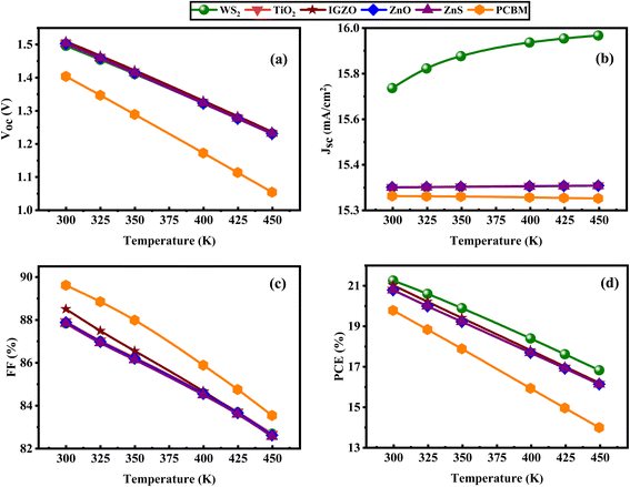
3.2.8 Impact of temperature. The device's performance was assessed within a temperature range of 300 K to 450 K. Analyzing the stability of solar cells requires understanding their performance under elevated thermal conditions. Fig. 14 demonstrates how temperature affects six distinct PSC configurations. It reveals that changes in temperature result in variations in VOC, JSC, FF, and PCE for each of the six configurations. Fig. 14a, c and d shows that the VOC, FF, and PCE decline as the temperature increases. However, the device with WS2 ETL exhibits a slightly higher JSC with rising temperatures, as shown in Fig. 14b. In our investigation, the JSC values of TiO2, IGZO, ZnO, and ZnS ETL-based structures were almost similar JSC, which was almost 15.34 mA cm−2. It can be observed that the WS2 ETL-based solar structure shows the highest JSC (≈15.78 mA cm−2), while the lowest value is observed in the PCBM (≈15.31 mA cm−2) ETL structure as shown in Fig. 14b. Solar cells using PCBM as the ETL exhibit the highest FF among the six ETL configurations, beginning at around 89.5%. Although the lowest FF values are observed in the IGZO ETL structure. Moreover, higher temperatures can lead to decreased VOC and PCE because of increased carrier recombination. As temperatures increase, both the diffusion length and Rs are affected, leading to an almost immediate impact on the FF and PCE of the device.113,115 As illustrated in Fig. 14a, the VOC for all six structures followed a consistent downward trend with increasing temperature. The PCBM ETL PSC exhibited the lowest VOC of about 1.40 V, while the remaining five ETL PSCs showed a higher VOC, approximately 1.5 V. In our analysis, it can be seen that the WS2, TiO2, IGZO, ZnO and ZnS ETLs structure showed almost above 20.25% PCE while the PCBM ETL showed about 19.24% PCE, which was almost reduced efficiency (Fig. 14d). The decrease in VOC for all optimal device configurations with higher temperatures is attributed to the inverse correlation between VOC and the reverse saturation current density (J0). As the temperature rises, J0 increases, as detailed in eqn (20)| |
 | (20) |
whereas  represents the thermal voltage. As the temperature of the PSC increases, the number of defects rises and the VOC decreases, consistent with previous research.116 A noticeable decline in short-circuit performance with increasing temperature is evident in Fig. 14a–d.
 |
| | Fig. 14 Temperature's impact on performance metrics (a) VOC, (b) JSC, (c) FF, (d) PCE of (ITO/ETL/LiMgI3/Cu2O/Ni) ETL = WS2, TiO2, IGZO, ZnO, ZnS, and PCBM. | |
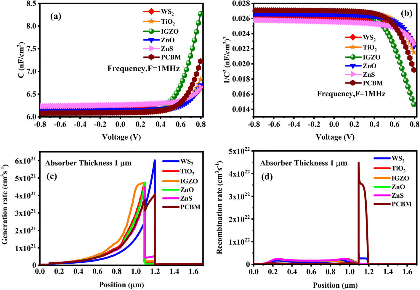
3.2.9 Analysis of capacitance and Mott–Schottky (MS). The influence of voltage, ranging from −0.8 to 0.8 V, on capacitance and Mott–Schottky (M–S) properties is demonstrated in Fig. 15a and b. Through capacitance–voltage (C–V) measurements, the M–S analytical approach facilitates the calculation of built-in voltage (Vbi) and charge carrier density (Nd). The junction capacitance per unit area (C) is deduced from eqn (21).| |
 | (21) |
Here, ε0 refers to the vacuum permittivity, εr represents the dielectric constant of the donor material, q denotes the electronic charge, and V is the applied voltage (Fig. 15b).117,118 The gradient of the linear part reveals Nd, and the built-in voltage Vbi is found by extending the line to the voltage axis. Fig. 15a and b illustrate that the frequency remains constant at 1 MHz while the voltage varies from −0.8 V to 0.8 V. The device coupled with IGZO and PCBM ETL exhibits voltage-independent capacitance between −0.8 V and 0.8 V. In Fig. 15a, it is observed that the capacitance of structures with WS2, TiO2, ZnO, and ZnS ETLs remains unaffected by changes in voltage, indicating that the depletion layer capacitance dominates as the applied voltage increases.119 Therefore, the dependence of capacitance on the applied voltage indicates the potential for using the device as a voltage-regulated SC. The Mott–Schottky method, known for its reliability and widespread use, enables the calculation of the built-in potential (Vbi) by investigating the difference between electrode performance and doping concentration.120 The well-reliable and recognized Mott–Schottky analysis is used to analyze the Vbi.121
 |
| | Fig. 15 Investigation of (a) capacitance (C), (b) Mott–Schottky (1/C2) trends, (c) charge generation rate, and (d) recombination rate for all six configurations. | |
The Mott–Schottky (M–S) method, emphasizing capacitance–voltage characteristics, is a well-established approach for analyzing space charge distributions in semiconductors, such as those due to junction capacitance.122 Our analysis indicates that Fig. 15b follows a unique trend, differing from the earlier figure. In this case, the voltage decreases linearly from −0.8 to 0.8 V for all six PSCs, which is in agreement with other studies.123,124 For PCBM and IGZO-based ETLs, M–S values started to decrease after reaching certain voltages, specifically beyond 0.4 V for PCBM and 0.5 V for IGZO. Conversely, the structures utilizing WS2, TiO2, ZnO, and ZnS ETLs showed a decrease in capacitance only after exceeding 0.6 V, as shown in Fig. 15b.
3.2.10 Influence of generation and recombination rate. The generation rate of a SC depends on both the location within the device and the wavelength of the incident light. It reflects the number of electron–hole pairs generated at each point due to photon absorption at specific wavelengths. This generation rate is essential for optimizing the efficiency of solar cells.125 The graphical depiction of the generation and recombination rates for the six layouts is presented in Fig. 15c and d. In the carrier generation process, electron–hole pairs are formed when electrons move from the valence band to the conduction band. For all six designs, Fig. 15c displays that the generation rates peak at 1.2 μm for WS2 configuration. The electron–hole pair generation, G(x), is calculated using the incoming photon flux, Nphot(λ,x), and SCAPS-1D as described in eqn (22):| | |
G(λ,x) = α(λ,x)Nphot(λ,x)
| (22) |
Recombination occurs when electrons in the conduction band and holes recombine and are effectively annihilated, which is the reverse process of generation.74 During recombination, the defect characteristics of each layer play a crucial role, resulting in the formation of energy states that have a substantial impact on the recombination process. It can be seen in Fig. 15d that the WS2, TiO2, IGZO, ZnO and ZnS ETL-based structures experience a delayed start in their recombination process. In Fig. 15d, the structure shows its optimal recombination rates between (1.1 and 1.2) for ITO/PCBM/LiMgI3/Cu2O/Ni configurations. Fig. 15d distinctly indicate that the PCBM as an ETL-based solar structure showed the highest recombination rate at the position of around 1.2 μm. In the range from 1.1 to 1.2 μm, an increased recombination rate is observed because more electrons from the conduction band transition across the energy barrier to occupy valence band positions. This shift affects the recombination rate of electron–hole pairs in the solar device.
3.2.11 JV and QE characteristics. Current density measures the electric current passing through a specific area and is essential for evaluating device performance. Fig. 16a illustrates the current–voltage density for an ITO/ETL/LiMgI3/Cu2O/Ni device configuration across six different ETLs. The voltage is supplied between 0 and 1.8 V. Firstly, the photocurrent values in all six combinations are nearly identical. All structures follow the same pattern between 0.0 and 1.5 V. Subsequently, WS2, TiO2, IGZO, ZnO, and ZnS PSCs experience a decrease in photocurrent around 1.4–1.6 V. Conversely, PCBM PSC experience a decrease in photocurrent around 1.3–1.4 V. It can be seen that in the initial optimization WS2, TiO2, IGZO, ZnO, and ZnS ETLs showed better J–V characteristics (in terms of JSC and VOC) for the solar structure than the PCBM ETLs. Initially, the photocurrent of the five (WS2, TiO2, IGZO, ZnO, and ZnS) PSCs is high JSC approximately >15.32 mA cm−2 when the VOC was about (0–1.5 V). However, the PCBM ETLs associated structure lowest JSC value of 15.31 mA cm−2, when the VOC was about (0–1.4 V). To accurately assess the photovoltaic parameters of a PSC, it is crucial to understand electron–hole recombination behaviors. The J–V curve of a perovskite layer reflects this understanding. Fig. 16b illustrates the correlation between the wavelength and quantum efficiency (QE) of the optimized device WS2, TiO2, IGZO, ZnO, ZnS, and PCBM ETLs. Here, the wavelength is adjusted between 300 and 900 nm. The QE charts for each device under investigation are represented in Fig. 16b. When the wavelength was 360 nm, the six PSCs had the best QE of (97–99%). When the wavelength was about 610 nm, all the PSCs displayed the optimal QE is 92%. Recombination diminishes the QE in solar cells when charge carriers are unable to reach the external circuit. Factors affecting the collection probability also have a significant impact on QE. For instance, carriers produced near the surface may be influenced by modifications to the front surface. At longer wavelengths, free carrier absorption in heavily doped surface layers can lead to a reduction in quantum efficiency.122 The study reveals that with rising voltage, the QE improves due to reduced recombination. Subsequently, QE starts to fall as the wavelength changes across all configurations. An increase in absorber thickness usually results in better QE, as a larger absorber can absorb a greater number of photons.126
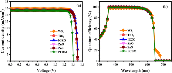 |
| | Fig. 16 (a) J–V characteristics and (b) QE response of the single halide PSCs. | |
3.2.12 Optimization of absorber/ETL interface layer defect density. The effect of defect density (Nt) at the interface between ETLs and the LiMgI3 absorber on photovoltaic characteristics such as VOC, JSC, FF, and PCE is shown in Fig. 17, with defect densities ranging from 1010 to 1018 cm−2. Fig. 17 shows that when Nt grows, the performance parameters of PSCs decrease due to higher recombination rates, resulting in a decrease in PCE. Specifically, VOC, JSC, FF, and PCE remain almost constant when Nt is ≤1013 cm−2, but they slightly decline (WS2, TiO2, IGZO, ZnO and PCBM) when Nt reaches ≥1014 cm−2. For a WS2-based ETL structure, VOC drops from approximately ∼1.49 to 1.43 V, JSC drop from ∼15.78 to 8.43 mA cm−2, FF increases from ∼87.80 to 87.90%, and subsequently, the PCE decreases from ∼20.73 to ∼10.69%. Solar cell heterostructures with TiO2, IGZO, ZnO, and PCBM ETLs demonstrate enhanced performance when the ETLs/LiMgI3 interface has a defect density (Nt) of ≤1 × 1013 cm−2. Among the five ETLs (WS2, TiO2, IGZO, ZnO, and PCBM), VOC, JSC, FF, and PCE show similar trends, whereas the ZnS ETL-based structure consistently maintains stable values. Therefore, it is concluded that a defect density of 1010 cm−2 is optimal for subsequent analyses and should be maintained to achieve the best results. The range of Nt was chosen for VOC analysis due to its higher sensitivity to defect density compared to JSC. The interface recombination limit for VOC can be defined using eqn (23).127| |
 | (23) |
where St signifies the recombination velocity at the interface. A denotes the ideality factor, and ∅c represents the effective barrier height.
 |
| | Fig. 17 Investigating the influence of ETL/LiMgI3 interface defect levels on VOC (V), JSC (mA cm−2), FF (%), and PCE (%) of LiMgI3. | |
3.2.13 Nyquist plot. The real and imaginary impedance components (Zre and Zim) for several ETLs are depicted in the Nyquist plot in Fig. 18. The behavior of different halide-based perovskite materials can be effectively studied using impedance analysis techniques.102 The Y-axis of this plot represents the geometrical capacitance, indicating where carriers accumulate at the interface layers, while the X-axis shows the resistance associated with recombination. Each plot exhibits a single semi-circle, process within the frequency range of 1 Hz to 1 MHz. The real (Zre) and imaginary (Zim) parts of impedance are plotted against each other. Nyquist plot provides an in-depth qualitative analysis of resistive losses, capacitance, and recombination defects affecting the device.128 The expanded semi-circle in the IGZO ETL-based structure indicates higher resistance indicates increased impedance or resistance. The WS2 ETL-based structure demonstrates a smaller semi-circle, which reflects lower impedance, smoother charge transport, and better interface characteristics compared to other ETLs. The TiO2, ZnO, ZnS, and PCBM ETLs had a similar trend. However, the Nyquist plot is observed in the case of TiO2, IGZO, ZnO, and ZnS ETL-based structures, which were much lower than WS2 structures but also higher than PCBM structures (Fig. 18). The resistance observed at high frequencies is related to the material's recombination resistance. Additionally, the capacitance measured at these frequencies reflects the geometric capacitance resulting from charge accumulation at the interfaces.129 In high-frequency measurements, the resistance observed is indicative of the material's recombination resistance. At the same time, the capacitance at these frequencies represents the geometric capacitance, which is associated with the accumulation of charge at the interfaces.130
 |
| | Fig. 18 Nyquist plot of the various ETL materials (WS2, TiO2, IGZO, ZnO, ZnS, and PCBM) based structure with LiMgI3 absorber. | |
3.2.14 Comparison of SCAPS-1D results with previous work. The performance parameters of the six device configurations examined in this study are compared with the most recently published optimal configurations in Table 6. According to Table 6, the LiMgI3 single halide perovskite-based solar cell presented here has a higher PCE value than the same-series device structures reported in earlier publications. The presented device structures utilizing WS2, IGZO, TiO2, ZnO, ZnS, and PCBM as ETLs achieved PCE values of 20.73%, 20.50%, 20.25%, 20.26%, 20.26%, and 19.47%, respectively. This is significantly higher than the previously published and FTO/SnS2/KGeCl3/Cu2O structure, which reported a PCE of approximately 15.83%.53 FTO/TiO2/CsSnI3/m-MTDATA/Au structure shows around 2.02% PCE.131 The VOC values of the presented solar structures are almost similar except the FTO/TiO2/KSnI3/Spiro-OMeTAD/Au structure is less than the previous published device configurations. In our same series of previously published device structures the ITO/TiO2/MASnI3/Spiro-OMeTAD/Au, ITO/PCBM/CsSnI3/NiO2/Al, and ITO/PCBM/CsSnI3/CuI/Au show lowest JSC than – LiMgI3 base device structure. All presented solar structures show a JSC of greater than 15 mA cm−2 except FTO/SnS2/KGeCl3/Cu2O, FTO/C60/KGeCl3/PEDOT:PSS, and C60/CsGeCl3/PEDOT:PSS structure.53,132 The FF values of the LiMgI3-based solar structure are much higher than those of the previously published device structure. Table 6 shows that the presented six solar structures show more effective performance than the previously reported solar cells. Table 6 reveals that the six solar cell configurations presented here are more efficient than previously reported CsSnI3-based solar cells, which had efficiency levels below 16%, while our LiMgI3 absorber achieves much higher performance. The first six LiMgI3-based solar cell device structures of Table 6 used a different ETL which shows higher efficiency than our previously published device structure. We examined absorber characteristics such as thickness, which differ from those in previous theoretical studies of device structures. Additionally, the ETL and HTL combinations we studied do not align with the properties of those previously explored in theoretical research. In addition, the optical properties change from one absorber to another, resulting in differences in solar energy absorption. The LiMgI3 absorber we examined demonstrated superior optical properties, as evidenced by the 20.73% PCE performance in the ITO/WS2/LiMgI3/Cu2O/Ni structure.133 Based on these factors, we can infer that our LiMgI3 solar cell exhibits a higher PCE compared to similar structured absorbers solar cells.
Table 6 PV performance parameters of our simulated configurations of LiMgI3a
| Optimized devices |
Types |
VOC (V) |
JSC (mA cm−2) |
FF (%) |
PCE (%) |
Ref. |
| Theo. = theoretical, Exp. = experimental. |
| ITO/WS2/LiMgI3/Cu2O/Ni |
Theo. |
1.49 |
15.78 |
87.81 |
20.73 |
This work |
| ITO/IGZO/LiMgI3/Cu2O/Ni |
Theo. |
1.50 |
15.34 |
88.48 |
20.50 |
This work |
| ITO/TiO2/LiMgI3/Cu2O/Ni |
Theo. |
1.50 |
15.34 |
87.89 |
20.25 |
This work |
| ITO/ZnO/LiMgI3/Cu2O/Ni |
Theo. |
1.50 |
15.34 |
87.86 |
20.26 |
This work |
| ITO/ZnS/LiMgI3/Cu2O/Ni |
Theo. |
1.50 |
15.34 |
87.81 |
20.26 |
This work |
| ITO/PCBM/LiMgI3/Cu2O/Ni |
Theo. |
1.41 |
15.36 |
89.49 |
19.47 |
This work |
| FTO/SnS2/KGeCl3/Cu2O |
Theo. |
0.545 |
41.91 |
69.24 |
15.83 |
53 |
| FTO/C60/KGeCl3/PEDOT:PSS |
Theo. |
0.702 |
31.29 |
65.36 |
14.37 |
132 |
| FTO/TiO2/RbGeBr3/P3HT/Au |
Theo. |
0.96 |
14.47 |
85.70 |
11.89 |
134 |
| C60/CsGeCl3/PEDOT:PSS |
Theo. |
0.703 |
21.39 |
64.60 |
9.8 |
132 |
| FTO/TiO2/KSnI3/Spiro-OMeTAD/Au |
Theo. |
1.70 |
15.85 |
36.13 |
9.77 |
135 |
| FTO/TiO2/CsSnI3/Au |
Exp. |
0.34 |
20.63 |
54.18 |
3.83 |
136 |
| FTO/TiO2/CsSnI3/m-MTDATA/Au |
Exp. |
0.24 |
22.70 |
0.37 |
2.02 |
131 |
| ITO/TiO2/MASnI3/Spiro-OMeTAD/Au |
Theo. |
0.88 |
16.80 |
0.42 |
6.40 |
137 |
| ITO/PCBM/CsSnI3/NiO2/Al |
Theo. |
0.52 |
10.21 |
62.50 |
3.31 |
138 |
| ITO/PCBM/CsSnI3/CuI/Au |
Theo. |
0.91 |
14.24 |
78.11 |
10.10 |
139 |
4 Conclusion
This work presents a comprehensive analysis of the optoelectronic and photovoltaic characteristics of LiMgI3 perovskite by integrating DFT and SCAPS-1D modeling. By employing first-principles calculations through density functional theory (DFT) for the first time, we comprehensively examined the structural, electrical, transport, and optical properties of LiMgI3, a single halide perovskite. The structural investigation indicates that LiMgI3 compounds possess a cubic structure. The lattice parameters and unit cell volume of LiMgI3 align with previous theoretical findings. The stability of this compound is demonstrated by its phonon dispersion curve. Through the analysis of the electrical band structure, it is evident that this material has an indirect band gap, confirming its semiconducting character. Moreover, the analysis of optical properties indicates the possible use of this particular perovskite in solar cells due to its extensive absorption capability and low energy band gap. The photovoltaic characteristics of this compound were investigated by using LiMgI3 as the absorber material in a single perovskite solar cell construction, with various ETL and HTL layers. Among the studied configurations, the ITO/WS2/LiMgI3/Cu2O/Ni structure demonstrated superior photovoltaic performance due to optimal band alignment, efficient charge extraction, and reduced recombination at interfaces. WS2 serves as an effective electron transport layer with good conductivity and stability, while Cu2O provides favorable valence band alignment with LiMgI3 for hole transport. This synergistic combination facilitates efficient carrier separation and transport, leading to enhanced device performance. The PCE of 20.73%, VOC of 1.49 V, JSC of 15.78 mA cm−2, and FF of 87.81% are observed in the ITO/Cu2O/LiMgI3/WS2/Ni combination. The thickness of the absorber and ETL has been varied to optimize the device's performance. The impact of series resistance, shunt resistance, and temperature on device performance are explored in this investigation. A decreasing nature of efficiency has been seen with increasing series resistance and temperature which is inverse in the case of shunt resistance. In addition, we incorporate Mott–Schottky and capacitance analyses, as well as the generation and recombination rates, into our investigation. The properties of QE and JV are also addressed. The efficiency of the device has been seen to be significantly impacted by the interface defect density. These findings are crucial for researchers studying single halide perovskite-based PSC because they allow for the creation of suitable SC configurations before the production and testing of these devices.
4.1 Limitation
While LiMgI3-based perovskites show promising theoretical optoelectronic properties, several practical challenges must be addressed before realizing efficient and scalable solar cells. One key concern is the chemical stability of LiMgI3 under ambient conditions, as the presence of lithium and iodine may lead to high sensitivity to moisture, oxygen, and temperature.140 This could necessitate encapsulation techniques or processing in an inert atmosphere. However, such issues are common with emerging perovskite materials and can be effectively managed through further experimental optimization and material engineering.
4.2 Future work
This analysis highlights a number of prospective paths for continuing the research:
(1) The absorber layer LiMgI3 demonstrates diverse qualities and promising behavior in photovoltaic applications, suggesting its suitability for use in multi-junction solar cell configurations.
(2) To explore whether incorporating a window layer, buffer layer, or other design elements can enhance solar cell efficiency without exceeding the theoretical limit of 33%-a new lead halide hetero-structure solar cell utilizing LiMgI3 could be engineered.
(3) The economic feasibility of producing LiMgI3-based solar cells largely depends on the scalability of the synthesis and fabrication processes.
Data availability
Data will be made available upon request.
Author contributions
Md. Raihan Kabir: investigation, methodology, data curation, conceptualization, and writing the original manuscript; Nazmul Shahadath: formal analysis, methodology, data curation, conceptualization, and review-editing; Md. Tarekuzzaman: formal analysis, methodology, data curation, software, conceptualization, and review-editing; Md. Abu Bakkar Siddique: formal analysis, validation and review-editing; O. Alsalmi: data curation, validation, and formal analysis; Md. Rasheduzzaman: formal analysis, validation, and review-editing; Md Abdul Qader: formal analysis and review-editing; M. Moazzam Hossen: formal analysis and review-editing; Md. Zahid Hasan: formal analysis, data curation, validation, supervision, and review-editing.
Conflicts of interest
There is no conflict to declare.
Abbreviations
| DFT | Density functional theory |
| PVSK | Perovskite |
| PSC | Perovskite solar cell |
| PCE | Power conversion efficiency |
| JSC | Short-circuit current density |
| VOC | Open-circuit voltage |
| FF | Fill factor |
| ETL/HTL | Electron/hole-transport layer |
| ITO | Indium tin oxide |
| PV | Photovoltaic |
| J–V | Current density–voltage |
| WS2 | Tungsten disulfide |
| TiO2 | Titanium dioxide |
| IGZO | Indium gallium zinc oxide |
| ZnO | Zinc oxide |
| ZnS | Zinc sulphide |
| PCBM | Phenyl-C61-butyric acid methyl ester |
| CuI | Copper iodide |
| Cu2O | Copper(I) oxide |
| CuO | Copper(II) oxide |
| CBTS | Copper barium tin sulfide |
| hν | Energy of photon |
| G(x) | Generation rate |
| n/p | Concentrations of electrons and holes |
| WF | Work function |
 | Effective mass of the electron/hole |
| Fn/p | Fermi level of the electron/hole |
| Ni | Nickel |
| EC/EV | Energy level of the conduction/valence band |
| PTAA | Poly(triarylamine) |
| PEDOT:PSS | Poly(3,4-ethylene-dioxythiophene):polystyrene sulfonate |
| CuSCN | Copper(I) thiocyanate |
| CdTe | Cadmium telluride |
| P3HT | Poly(3-hexylthiophene-2,5-diyl) |
| Spiro-OMeTAD | 2,2′,7,7′-Tetrakis[N,N-di(4-methoxyphenyl)amino]-9,9′-spirobifluorene |
| SCAPS | Solar cell capacitance simulator |
Acknowledgements
The authors extend their appreciation to Umm Al-Qura University, Saudi Arabia for funding this research work through grant number: 25UQU4300099GSSR06. Funding statement: This research work was funded by Umm Al-Qura University, Saudi Arabia under grant number: 25UQU4300099GSSR06.
References
- O. Ellabban, H. Abu-Rub and F. Blaabjerg, Renewable Sustainable Energy Rev., 2014, 39, 748–764 Search PubMed.
- K. Dedecker and G. Grancini, Adv. Energy Mater., 2020, 10, 2001471 CrossRef CAS.
- I. Hamideddine, H. Jebari, N. Tahiri, O. El Bounagui and H. Ez-Zahraouy, Int. J. Energy Res., 2022, 46, 20755–20765 Search PubMed.
- B. Padha, S. Verma, P. Mahajan and S. Arya, ECS Trans., 2022, 107, 12073–12081 CrossRef CAS.
- L. Calió, S. Kazim, M. Grätzel and S. Ahmad, Angew. Chem., Int. Ed., 2016, 55, 14522–14545 CrossRef PubMed.
- L. Chen, C. Li, Y. Zhao, J. Wu, X. Li, Z. Qiao, P. He, X. Qi, Z. Liu and G. Wei, Chem. Eng. J., 2021, 425, 131599 Search PubMed.
- S. Arya, P. Mahajan, R. Gupta, R. Srivastava, N. K. Tailor, S. Satapathi, R. R. Sumathi, R. Datt and V. Gupta, Prog. Solid State Chem., 2020, 60, 100286 Search PubMed.
- P. Mahajan, B. Padha, S. Verma, V. Gupta, R. Datt, W. C. Tsoi, S. Satapathi and S. Arya, J. Energy Chem., 2022, 68, 330–386 Search PubMed.
- P. Mahajan, R. Datt, W. Chung Tsoi, V. Gupta, A. Tomar and S. Arya, Coord. Chem. Rev., 2021, 429, 213633 CrossRef CAS.
- Y. Chen, L. Zhang, Y. Zhang, H. Gao and H. Yan, RSC Adv., 2018, 8, 10489–10508 Search PubMed.
- A. Kojima, K. Teshima, Y. Shirai and T. Miyasaka, J. Am. Chem. Soc., 2009, 131, 6050–6051 CrossRef CAS PubMed.
- M. Kulbak, D. Cahen and G. Hodes, J. Phys. Chem. Lett., 2015, 6, 2452–2456 CrossRef CAS PubMed.
- S. D. Stranks and H. J. Snaith, Nat. Nanotechnol., 2015, 10, 391–402 Search PubMed.
- Y. Zhou and K. Zhu, ACS Energy Lett., 2016, 1, 64–67 Search PubMed.
- Y. Zhou, M. Yang, S. Pang, K. Zhu and N. P. Padture, J. Am. Chem. Soc., 2016, 138, 5535–5538 CrossRef CAS PubMed.
- N. Saleh, S. Al-Trawneh, H. Al-Dmour, S. Al-Taweel and J. P. Graham, J. Fluoresc., 2015, 25, 59–68 CrossRef CAS PubMed.
- H. Al-Dmour, R. H. Alzard, H. Alblooshi, K. Alhosani, S. AlMadhoob and N. Saleh, Front. Chem., 2019, 7, 561 CrossRef CAS PubMed.
- T. Miyasaka, A. Kulkarni, G. M. Kim, S. Öz and A. K. Jena, Adv. Energy Mater., 2020, 10, 1902500 CrossRef CAS.
- P. Gao, M. Grätzel and M. K. Nazeeruddin, Energy Environ. Sci., 2014, 7, 2448–2463 Search PubMed.
- P. Zhao, J. Su, Z. Lin, J. Wang, J. Zhang, Y. Hao, X. Ouyang and J. Chang, Adv. Theory Simul., 2020, 3, 2000055 Search PubMed.
- H. Al-Dmour, D. M. Taylor and J. A. Cambridge, J. Phys. D: Appl. Phys., 2007, 40, 5034–5038 Search PubMed.
- H. Al-Dmour and D. M. Taylor, Appl. Phys. Lett., 2009, 94, 223309 Search PubMed.
- T. He, Y. Jiang, X. Xing and M. Yuan, Adv. Mater., 2020, 32, 1903937 CrossRef CAS PubMed.
- A. N. Singh, S. Kajal, J. Kim, A. Jana, J. Y. Kim and K. S. Kim, Adv. Energy Mater., 2020, 10, 2070129 CrossRef CAS.
- J. Xu, R. Saklatvala, S. Mittal, S. Deshmukh and A. Procopio, Advanced Science, 2020, 7, 1903394 Search PubMed.
- R. Sharma, A. Sharma, S. Agarwal and M. S. Dhaka, Sol. Energy, 2022, 244, 516–535 Search PubMed.
- G. Souadi, Inorg. Chem. Commun., 2024, 167, 112768 Search PubMed.
- A. S. Belousov, E. V. Suleimanov, I. Shafiq and H. Li, J. Environ. Chem. Eng., 2025, 13, 116750 CrossRef.
- S. K. Mitro, M. Saiduzzaman, A. Biswas, A. Sultana and K. M. Hossain, Mater. Today Commun., 2022, 31, 103532 CrossRef CAS.
- S. K. Mitro, M. Saiduzzaman, T. I. Asif and K. M. Hossain, J. Mater. Sci.: Mater. Electron., 2022, 33, 13860–13875 CrossRef CAS.
- D. Behera, B. Akila, S. K. Mukherjee, T. A. Geleta, A. Shaker and M. M. Salah, Crystals, 2023, 13, 1437 Search PubMed.
- M. M. Namisi, R. J. Musembi, W. M. Mulwa and B. O. Aduda, Comput. Condens. Matter., 2023, 34, e00772 Search PubMed.
- K. Wang, Z. Jin, L. Liang, H. Bian, D. Bai, H. Wang, J. Zhang, Q. Wang and S. Liu, Nat. Commun., 2018, 9, 4544 CrossRef PubMed.
- E. Smecca, Y. Numata, I. Deretzis, G. Pellegrino, S. Boninelli, T. Miyasaka, A. La Magna and A. Alberti, Phys. Chem. Chem. Phys., 2016, 18, 13413–13422 RSC.
- H. Al-Dmour and Department of Physics, Faculty of Science, Mutah University, AIMS Mater. Sci., 2021, 8, 261–270 Search PubMed.
- G. Tong, L. K. Ono and Y. Qi, Energy Technol., 2020, 8, 1900961 Search PubMed.
- S. Arya, A. Singh, A. Ahmed, B. Padha, A. Banotra, U. Parihar, A. K. Sundramoorthy, S. Dixit and N. I. Vatin, J. Energy Chem., 2025, 105, 193–223 CrossRef CAS.
- R. Kour, S. Arya, S. Verma, J. Gupta, P. Bandhoria, V. Bharti, R. Datt and V. Gupta, Glob. Chall., 2019, 3, 1900050 CrossRef PubMed.
- S. Arya, A. Sharma, A. Singh, A. Ahmed, A. Dubey, B. Padha, S. Khan, R. Mahadeva, A. Khosla and V. Gupta, ECS Sens. Plus, 2024, 3, 022601 CrossRef CAS.
- M. K. Hossain, M. T. Rahman, M. K. Basher, M. J. Afzal and M. S. Bashar, Results Phys., 2018, 11, 1172–1181 Search PubMed.
- M. K. Hossain, M. T. Rahman, M. K. Basher, M. S. Manir and M. S. Bashar, Optik, 2019, 178, 449–460 Search PubMed.
- H. Al Dmour, East Eur. J. Phys., 2023, 555–561 Search PubMed.
- A. M. D. A. Jaber, A. Alsoud, S. R. Al-Bashaish, H. Al Dmour, M. S. Mousa, T. Trčka, V. Holcman and D. Sobola, Technologies, 2024, 12, 87 CrossRef.
- Department of Physics, Faculty of Science, Mutah University, H. Al-Dmour, D. M. Taylor and School of Electronic Engineering, Bangor University, J. Ovonic Res., 2023, 587–596 Search PubMed.
- B. Gil, A. J. Yun, Y. Lee, J. Kim, B. Lee and B. Park, Electron. Mater. Lett., 2019, 15, 505–524 Search PubMed.
- K. Sobayel, Md. Akhtaruzzaman, K. S. Rahman, M. T. Ferdaous, Z. A. Al-Mutairi, H. F. Alharbi, N. H. Alharthi, M. R. Karim, S. Hasmady and N. Amin, Results Phys., 2019, 12, 1097–1103 Search PubMed.
- D. Shin, B. Saparov, T. Zhu, W. P. Huhn, V. Blum and D. B. Mitzi, Chem. Mater., 2016, 28, 4771–4780 Search PubMed.
- R. Chakraborty, K. M. Sim, M. Shrivastava, K. V. Adarsh, D. S. Chung and A. Nag, ACS Appl. Energy Mater., 2019, 2, 3049–3055 Search PubMed.
- C. Devi and R. Mehra, J. Mater. Sci., 2019, 54, 5615–5624 Search PubMed.
- M. K. Hossain, M. H. K. Rubel, G. F. I. Toki, I. Alam, Md. F. Rahman and H. Bencherif, ACS Omega, 2022, 7, 43210–43230 Search PubMed.
- D. Sabba, H. K. Mulmudi, R. R. Prabhakar, T. Krishnamoorthy, T. Baikie, P. P. Boix, S. Mhaisalkar and N. Mathews, J. Phys. Chem. C, 2015, 119, 1763–1767 Search PubMed.
- T.-B. Song, T. Yokoyama, J. Logsdon, M. R. Wasielewski, S. Aramaki and M. G. Kanatzidis, ACS Appl. Energy Mater., 2018, 1, 4221–4226 CrossRef CAS.
- Md. A. F. Siddique and A. S. Md. Sayem Rahman, Mater. Sci. Eng., B, 2024, 303, 117268 CrossRef CAS.
- F.-T. -Zahra, Md. M. Islam, Md. M. Hasan, Md. R. Islam and S. Ahmad, J. Phys. Chem. Solids, 2024, 191, 112037 CrossRef CAS.
- Md. T. Hossain, M. M. Hasan, F.-T. Zahra, S. Swargo, R. Al-Arefeen Dhroobo, Md. R. Al Amin, F. M. A. Sieam, S. T. Disha and Md. R. Islam, Phys. B, 2024, 690, 416131 Search PubMed.
- A. H. Mahedi, Md. S. Rahman, Md. Tarekuzzaman, H. Al-Dmour, Md. Rasheduzzaman, M. M. Hossen, Y. Arafat and Md. Z. Hasan, Sol. Energy, 2025, 289, 113338 CrossRef CAS.
- T. Das, G. Di Liberto and G. Pacchioni, J. Phys. Chem. C, 2022, 126, 2184–2198 CrossRef CAS.
- M. Ben Bechir and M. H. Dhaou, RSC Adv., 2021, 11, 21767–21780 RSC.
- N. L. Dey, Md. S. Reza, A. Ghosh, H. Al-Dmour, M. Moumita, Md. S. Reza, S. Sultana, A. K. M. Yahia, M. Shahjalal, N. S. Awwad and H. A. Ibrahium, J. Phys. Chem. Solids, 2025, 196, 112386 CrossRef CAS.
- S. J. Clark, M. D. Segall, C. J. Pickard, P. J. Hasnip, M. I. J. Probert, K. Refson and M. C. Payne, Z. Kristallogr.–Cryst. Mater., 2005, 220, 567–570 Search PubMed.
- M. D. Segall, P. J. D. Lindan, M. J. Probert, C. J. Pickard, P. J. Hasnip, S. J. Clark and M. C. Payne, J. Phys.: Condens. Matter, 2002, 14, 2717–2744 Search PubMed.
- J. Heyd, G. E. Scuseria and M. Ernzerhof, J. Chem. Phys., 2003, 118, 8207–8215 CrossRef CAS.
- J. P. Perdew, A. Ruzsinszky, G. I. Csonka, O. A. Vydrov, G. E. Scuseria, L. A. Constantin, X. Zhou and K. Burke, Phys. Rev. Lett., 2008, 100, 136406 CrossRef PubMed.
- D. Vanderbilt, Phys. Rev. B: Condens. Matter Mater. Phys., 1990, 41, 7892–7895 CrossRef PubMed.
- F. D. Murnaghan, Am. J. Math., 1937, 59, 235–260 CrossRef.
- T. H. Fischer and J. Almlof, J. Phys. Chem., 1992, 96, 9768–9774 CrossRef CAS.
- H. J. Monkhorst and J. D. Pack, Phys. Rev. B, 1976, 13, 5188–5192 Search PubMed.
- Md. Hasan Ali, A. T. M. Saiful Islam, M. D. Haque, Md. Ferdous Rahman, M. Khalid Hossain, N. Sultana and A. Z. M. Touhidul Islam, Mater. Today Commun., 2023, 34, 105387 CrossRef CAS.
- R. Pandey, S. Bhattarai, K. Sharma, J. Madan, A. K. Al-Mousoi, M. K. A. Mohammed and M. K. Hossain, ACS Appl. Electron. Mater., 2023, 5, 5303–5315 CrossRef CAS.
- A. K Al-Mousoi, M. K. A. Mohammed, S. Q. Salih, R. Pandey, J. Madan, D. Dastan, E. Akman, A. A. Alsewari and Z. M. Yaseen, Energy Fuels, 2022, 36, 14403–14410 CrossRef CAS.
- A. K. Al-Mousoi, M. K. A. Mohammed, R. Pandey, J. Madan, D. Dastan, G. Ravi, P. Sakthivel and G. A. Babu, RSC Adv., 2022, 12, 32365–32373 RSC.
- R. A. Jabr, M. Hamad and Y. Mohanna, Int. J. Electr. Eng. Educ., 2007, 44, 23–33 CrossRef.
- Y. H. Khattak, Modeling of high power conversion efficiency thin film solar cells, PhD thesis, Universitat Politècnica de València, 2019.
- M. K. Hossain, A. A. Arnab, R. C. Das, K. M. Hossain, M. H. K. Rubel, Md. F. Rahman, H. Bencherif, M. E. Emetere, M. K. A. Mohammed and R. Pandey, RSC Adv., 2022, 12, 34850–34873 RSC.
- C. Chen, X. Lu, X. Hu, G. Liang and G. Fang, J. Mater. Chem. C, 2024, 12, 16–28 RSC.
- Md. S. Reza, Md. F. Rahman, A. Kuddus, M. K. A. Mohammed, A. K. Al-Mousoi, Md. R. Islam, A. Ghosh, S. Bhattarai, R. Pandey, J. Madan and M. K. Hossain, RSC Adv., 2023, 13, 31330–31345 RSC.
- M. S. Uddin, M. K. Hossain, M. B. Uddin, G. F. I. Toki, M. Ouladsmane, M. H. K. Rubel, D. I. Tishkevich, P. Sasikumar, R. Haldhar and R. Pandey, Adv. Electron. Mater., 2024, 10, 2300751 CrossRef CAS.
- K. W. Guji, T. A. Geleta, N. Bouri and V. J. Ramirez Rivera, Nanoscale Adv., 2024, 6, 4479–4491 RSC.
- J. Li, Y. Liu, J. Bai, C. Xie, H. Yuan, Z. Cheng, W. Wang, X. Wang and G. Zhang, Applied Physics Reviews, 2023, 10, 031416 CrossRef CAS.
- J. W. Wafula, J. W. Makokha and G. S. Manyali, Results Phys., 2022, 43, 106132 CrossRef.
- M. Tarekuzzaman, M. H. Ishraq, M. A. Rahman, A. Irfan, M. Z. Rahman, M. S. Akter, S. Abedin, M. A. Rayhan, M. Rasheduzzaman, M. M. Hossen and M. Z. Hasan, J. Comput. Chem., 2024, 45(29), 2476–2500 CrossRef CAS PubMed.
- R. Geiger, T. Zabel and H. Sigg, Front. Mater., 2015, 2, 52 Search PubMed.
- S. Kerdsongpanya, B. Alling and P. Eklund, Phys. Rev. B: Condens. Matter Mater. Phys., 2012, 86, 195140 CrossRef.
- S. Mahmud, M. A. Ali, M. M. Hossain and M. M. Uddin, Vacuum, 2024, 221, 112926 CrossRef CAS.
- W. Kohn and L. J. Sham, Phys. Rev., 1965, 140, A1133–A1138 CrossRef.
- Q. Mahmood, U. Hani, T. I. Al-Muhimeed, A. A. AlObaid, B. Ul Haq, G. Murtaza, T. H. Flemban and H. Althib, J. Phys. Chem. Solids, 2021, 155, 110117 CrossRef CAS.
- A. J. Kale, R. Chaurasiya and A. Dixit, Adv. Theory Simul., 2021, 4, 2000224 CrossRef CAS.
- Md. M. Hossain, Md. A. Ali, Md. M. Uddin, S. H. Naqib and A. K. M. A. Islam, ACS Omega, 2021, 6, 33899–33913 CrossRef CAS PubMed.
- M. Roknuzzaman, M. A. Hadi, M. J. Abden, M. T. Nasir, A. K. M. A. Islam, M. S. Ali, K. Ostrikov and S. H. Naqib, Comput. Mater. Sci., 2016, 113, 148–153 CrossRef CAS.
- E. Keaney, J. Shearer, A. Panwar and J. Mead, J. Compos. Mater., 2018, 52, 3299–3307 CrossRef.
- M. A. Rashid, M. Saiduzzaman, A. Biswas and K. M. Hossain, Eur. Phys. J. Plus, 2022, 137, 649 CrossRef CAS.
- S. Hayat, R. M. A. Khalil, M. I. Hussain, A. M. Rana and F. Hussain, Solid State Commun., 2022, 344, 114674 CrossRef CAS.
- D. Pottmaier, E. R. Pinatel, J. G. Vitillo, S. Garroni, M. Orlova, M. D. Baró, G. B. M. Vaughan, M. Fichtner, W. Lohstroh and M. Baricco, Chem. Mater., 2011, 23, 2317–2326 CrossRef CAS.
- M. A. Hadi, M. Roknuzzaman, F. Parvin, S. H. Naqib, A. K. M. A. Islam and M. Aftabuzzaman, J. Sci. Res, 2013, 6, 11–27 CrossRef.
- Md. Tarekuzzaman, N. Shahadath, M. Montasir, O. Alsalmi, M. H. Mia, H. Al-Dmour, Md. Rasheduzzaman and Md. Z. Hasan, RSC Adv., 2025, 15, 13643–13661 RSC.
- M. Manzoor, A. Tewari, S. Ansar, Y. A. Kumar and R. Sharma, J. Inorg. Organomet. Polym., 2025, 35, 795–812 CrossRef CAS.
- M. Born, Math. Proc. Cambridge Philos. Soc., 1940, 36, 160–172 CrossRef CAS.
- M. Born and K. Huang, Dynamical Theory of Crystal Lattices, Oxford University Press, Oxford, 1954 Search PubMed.
- Md. T. Hossain, J. Islam, M. Hasan and K. Hossain, Phys. B, 2024, 691, 416355 CrossRef CAS.
- R. Darolia, Int. Mater. Rev., 2013, 58, 315–348 Search PubMed.
- T. Kim, J. Lim and S. Song, Energies, 2020, 13, 5572 CrossRef CAS.
- K. Sekar, L. Marasamy, S. Mayarambakam, H. Hawashin, M. Nour and J. Bouclé, RSC Adv., 2023, 13, 25483–25496 RSC.
- M. R. Kabir, M. H. Ishraq, M. Tarekuzzaman, N. I. Nahid, J. K. Modak, S. Ahmad, A. M. Arfi, M. Rasheduzzaman and M. Z. Hasan, Eng. Res. Express, 2025, 7, 015319 CrossRef.
- K. Sekar, L. Marasamy, S. Mayarambakam, H. Hawashin, M. Nour and J. Bouclé, RSC Adv., 2023, 13, 25483–25496 RSC.
- M. K. Hossain, M. K. A. Mohammed, R. Pandey, A. A. Arnab, M. H. K. Rubel, K. M. Hossain, M. H. Ali, Md. F. Rahman, H. Bencherif, J. Madan, Md. R. Islam, D. P. Samajdar and S. Bhattarai, Energy Fuels, 2023, 37, 6078–6098 CrossRef CAS.
- M. K. Hossain, A. A. Arnab, D. P. Samajdar, M. H. K. Rubel, M. M. Hossain, Md. R. Islam, R. C. Das, H. Bencherif, Md. F. Rahman, J. Madan, R. Pandey, S. Bhattarai, M. Amami and D. K. Dwivedi, Energy Fuels, 2023, 37, 13377–13396 CrossRef CAS.
- M. Khalid Hossain, G. F. Ishraque Toki, I. Alam, R. Pandey, D. P. Samajdar, M. Ferdous Rahman, M. Rasidul Islam, M. H. K. Rubel, H. Bencherif, J. Madan and M. K. A. Mohammed, New J. Chem., 2023, 47, 4801–4817 RSC.
- D. Jayan K, V. Sebastian and J. Kurian, Sol. Energy, 2021, 221, 99–108 CrossRef CAS.
- J. D. Servaites, S. Yeganeh, T. J. Marks and M. A. Ratner, Adv. Funct. Mater., 2010, 20, 97–104 CrossRef CAS.
- E. E. Van Dyk and E. L. Meyer, Renewable Energy, 2004, 29, 333–344 CrossRef CAS.
- K. Tvingstedt, L. Gil-Escrig, C. Momblona, P. Rieder, D. Kiermasch, M. Sessolo, A. Baumann, H. J. Bolink and V. Dyakonov, ACS Energy Lett., 2017, 2, 424–430 CrossRef CAS.
- Y. Li, B. Ding, Q.-Q. Chu, G.-J. Yang, M. Wang, C.-X. Li and C.-J. Li, Sci. Rep., 2017, 7, 46141 CrossRef CAS PubMed.
- S. R. Raga, E. M. Barea and F. Fabregat-Santiago, J. Phys. Chem. Lett., 2012, 3, 1629–1634 CrossRef CAS PubMed.
- A. Sunny, S. Rahman, M. M. Khatun and S. R. A. Ahmed, AIP Adv., 2021, 11, 065102 CrossRef CAS.
- F. Behrouznejad, S. Shahbazi, N. Taghavinia, H.-P. Wu and E. Wei-Guang Diau, J. Mater. Chem. A, 2016, 4, 13488–13498 RSC.
- M. K. Hossain, M. H. K. Rubel, G. F. I. Toki, I. Alam, Md. F. Rahman and H. Bencherif, ACS Omega, 2022, 7, 43210–43230 CrossRef CAS PubMed.
- S. Lin, Bell Syst. Tech. J., 1965, 44, 2245–2269 CrossRef.
- X. Zhang, X. Chen, Y. Chen, N. A. Nadege Ouedraogo, J. Li, X. Bao, C. B. Han, Y. Shirai, Y. Zhang and H. Yan, Nanoscale Adv., 2021, 3, 6128–6137 RSC.
- Md. Samiul Islam, K. Sobayel, A. Al-Kahtani, M. A. Islam, G. Muhammad, N. Amin, Md. Shahiduzzaman and Md. Akhtaruzzaman, Nanomaterials, 2021, 11, 1218 CrossRef PubMed.
- E. H. Jung, N. J. Jeon, E. Y. Park, C. S. Moon, T. J. Shin, T.-Y. Yang, J. H. Noh and J. Seo, Nature, 2019, 567, 511–515 CrossRef CAS PubMed.
- M. Y. Rahman and S. M. Mominuzzaman, Exploring Lead Free Mixed Halide Double Perovskites Solar Cell, arXiv, 2024, preprint, arXiv:2401.09584, DOI:10.48550/arXiv.2401.09584.
- M. K. Hossain, M. K. A. Mohammed, R. Pandey, A. A. Arnab, M. H. K. Rubel, K. M. Hossain, M. H. Ali, Md. F. Rahman, H. Bencherif, J. Madan, Md. R. Islam, D. P. Samajdar and S. Bhattarai, Energy Fuels, 2023, 37, 6078–6098 CrossRef CAS.
- G. G. Malliaras, J. R. Salem, P. J. Brock and C. Scott, Phys. Rev. B: Condens. Matter Mater. Phys., 1998, 58, R13411–R13414 CrossRef CAS.
- A. A. Goje, N. A. Ludin, M. A. Mat Teridi, U. Syafiq, M. A. Ibrahim, F. Nawab and A. A. Syakirin, IOP Conf. Ser.: Mater. Sci. Eng., 2023, 1278, 012004 CrossRef CAS.
- M. K. Hossain, D. P. Samajdar, R. C. Das, A. A. Arnab, Md. F. Rahman, M. H. K. Rubel, Md. R. Islam, H. Bencherif, R. Pandey, J. Madan and M. K. A. Mohammed, Energy Fuels, 2023, 37, 3957–3979 CrossRef CAS.
- Mamta, K. K. Maurya and V. N. Singh, J. Sci.: Adv. Mater. Devices, 2022, 7(2), 100445 Search PubMed.
- N. Jensen, R. M. Hausner, R. B. Bergmann, J. H. Werner and U. Rau, Prog. Photovoltaics, 2002, 10, 1–13 CAS.
- S. Bhattarai, R. Pandey, J. Madan, S. Tayeng, P. K. Kalita, M. Z. Ansari, L. Ben Farhat, M. Amami and M. K. Hossain, RSC Adv., 2023, 13, 26851–26860 RSC.
- E. Von Hauff and D. Klotz, J. Mater. Chem. C, 2022, 10, 742–761 RSC.
- A. Guerrero, J. Bisquert and G. Garcia-Belmonte, Chem. Rev., 2021, 121, 14430–14484 CrossRef CAS PubMed.
- M. H. Kumar, S. Dharani, W. L. Leong, P. P. Boix, R. R. Prabhakar, T. Baikie, C. Shi, H. Ding, R. Ramesh, M. Asta, M. Graetzel, S. G. Mhaisalkar and N. Mathews, Adv. Mater., 2014, 26, 7122–7127 Search PubMed.
- C. Li and I. Tlili, Eng. Anal. Bound. Elem., 2023, 155, 425–431 CrossRef.
- K. Deepthi Jayan and V. Sebastian, in 2021 7th International Conference on Electrical Energy Systems (ICEES), 2021, pp. 623–628 Search PubMed.
- S. Valizadeh, A. Shokri, A. Sabouri-Dodaran, N. Fough and F. Muhammad-Sukki, Results Phys., 2024, 57, 107351 Search PubMed.
- G. Pindolia, S. M. Shinde and P. K. Jha, Mater. Chem. Phys., 2023, 297, 127426 Search PubMed.
- T.-B. Song, T. Yokoyama, J. Logsdon, M. R. Wasielewski, S. Aramaki and M. G. Kanatzidis, ACS Appl. Energy Mater., 2018, 1, 4221–4226 Search PubMed.
- N. K. Noel, S. D. Stranks, A. Abate, C. Wehrenfennig, S. Guarnera, A.-A. Haghighirad, A. Sadhanala, G. E. Eperon, S. K. Pathak, M. B. Johnston, A. Petrozza, L. M. Herz and H. J. Snaith, Energy Environ. Sci., 2014, 7, 3061–3068 Search PubMed.
- N. Wang, Y. Zhou, M. Ju, H. F. Garces, T. Ding, S. Pang, X. C. Zeng, N. P. Padture and X. W. Sun, Adv. Energy Mater., 2016, 6, 1601130 Search PubMed.
- M. K. Hossain, G. F. I. Toki, D. P. Samajdar, M. Mushtaq, M. H. K. Rubel, R. Pandey, J. Madan, M. K. A. Mohammed, Md. R. Islam, Md. F. Rahman and H. Bencherif, ACS Omega, 2023, 8, 22466–22485 Search PubMed.
- J. Zhuang, J. Wang and F. Yan, Nano-Micro Lett., 2023, 15, 84 Search PubMed.
|
| This journal is © The Royal Society of Chemistry 2025 |
Click here to see how this site uses Cookies. View our privacy policy here. 
 Open Access Article
 This Open Access Article is licensed under a Creative Commons Attribution-Non Commercial 3.0 Unported Licence
 ab,
Md. Abu Bakkar Siddiqueab,
O. Alsalmic,
Md. Rasheduzzamanab,
Md Abdul Qaderd,
M. Moazzam Hossen
ab,
Md. Abu Bakkar Siddiqueab,
O. Alsalmic,
Md. Rasheduzzamanab,
Md Abdul Qaderd,
M. Moazzam Hossen

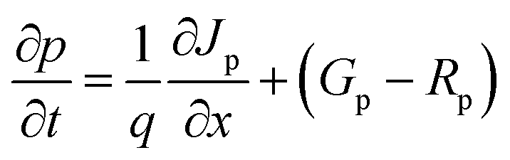


 and electron mass
  as 0.321m0 and 0.0393m0, respectively. This material is most likely p-type since it has a higher effective hole mass
  than electron mass
  Reduced effective mass facilitates carrier transport, making it ideal for solar materials.84 The following formula uses the effective masses to determine the mobility (μe for electrons and μh for holes).85

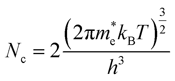


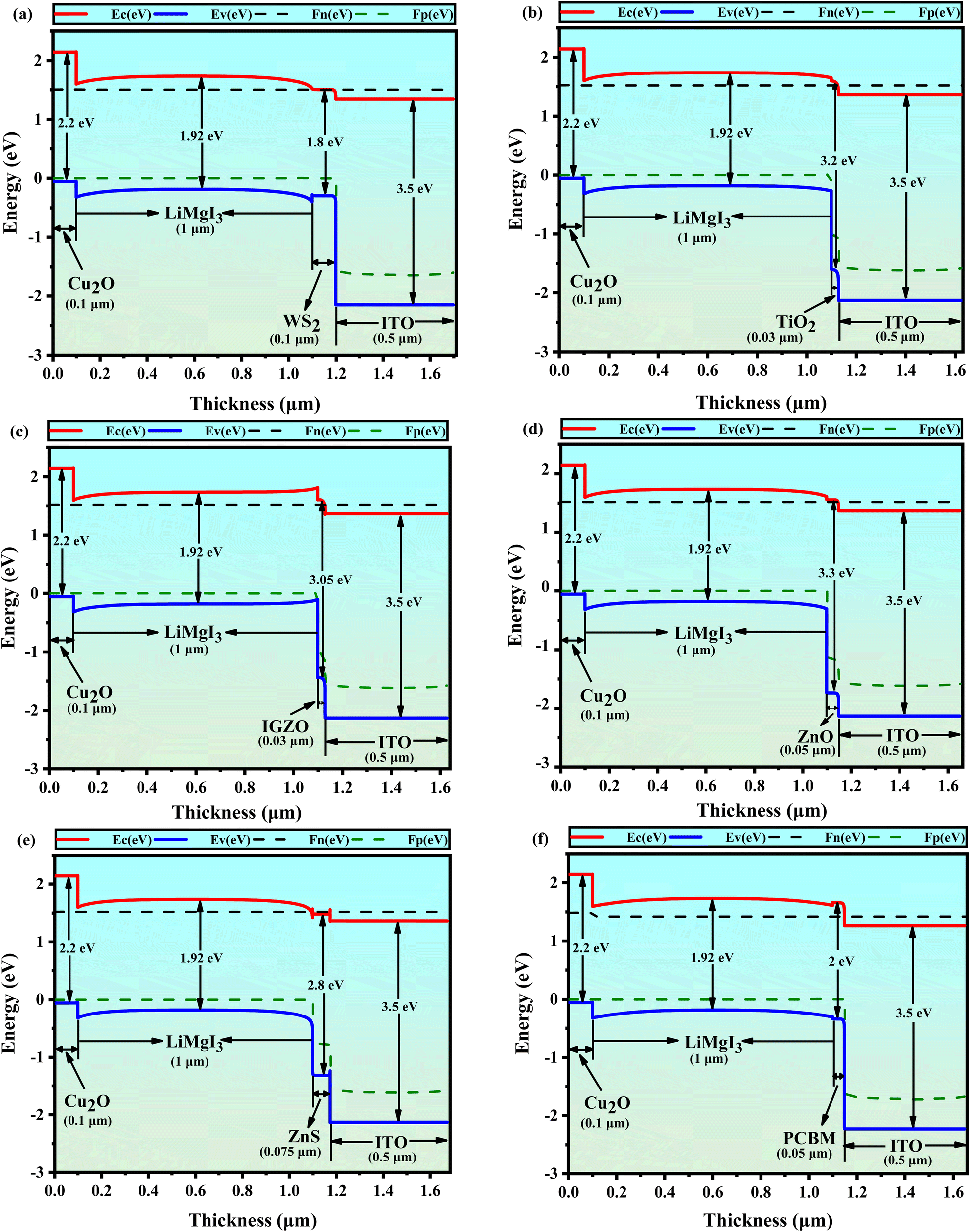


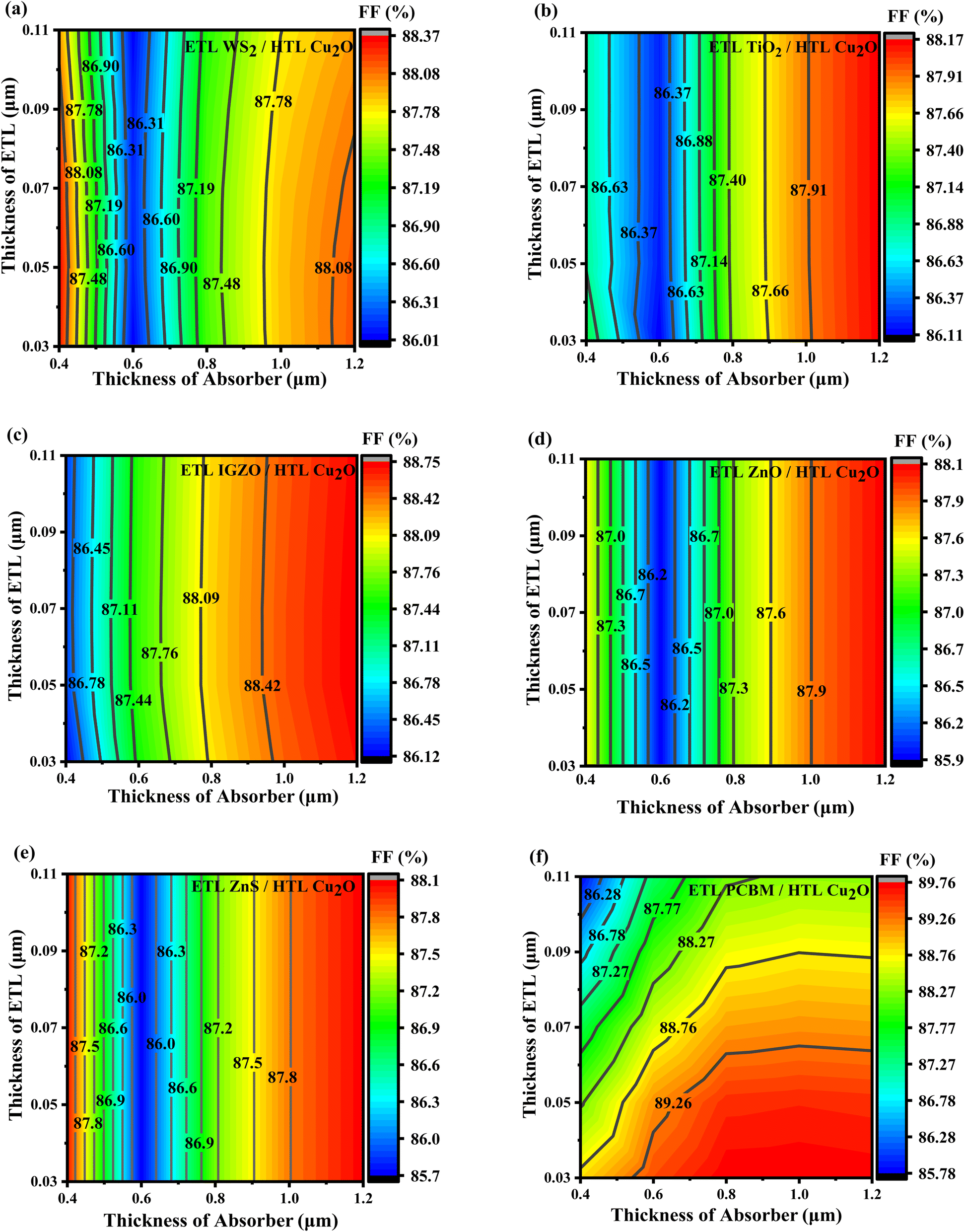


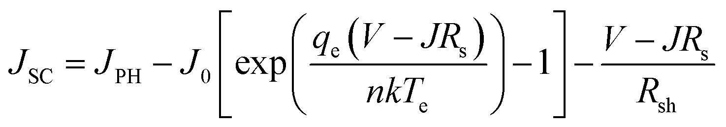


 represents the thermal voltage. As the temperature of the PSC increases, the number of defects rises and the VOC decreases, consistent with previous research.116 A noticeable decline in short-circuit performance with increasing temperature is evident in Fig. 14a–d.