DOI:
10.1039/D3NH00407D
(Communication)
Nanoscale Horiz., 2024,
9, 254-263
Microelectromechanical system for in situ quantitative testing of tension–compression asymmetry in nanostructures†
Received
18th September 2023
, Accepted 21st November 2023
First published on 21st November 2023
Abstract
Tension–compression asymmetry is a topic of current interest in nanostructures, especially in strain engineering. Herein, we report a novel on-chip microelectromechanical system (MEMS) that can realize in situ quantitative mechanical testing of nanostructures under tension–compression functions. The mechanical properties of three kinds of nanostructures fabricated by focused ion beam (FIB) techniques were systematically investigated with the presented on-chip testing system. The results declare that both Pt nanopillars and C nanowires exhibit plastic deformation behavior under tension testing, with average Young's moduli of 70.06 GPa and 58.32 GPa, respectively. However, the mechanical deformation mechanisms of the two nanostructures changed in compression tests. The Pt nanopillar exhibited in-plane buckling behavior, while the C nanowire displayed 3D twisting behavior with a maximum strain of 25.47%, which is far greater than the tensile strain. Moreover, asymmetric behavior was also observed in the C nanospring during five loading–unloading tension–compression deformation tests. This work provides a novel insight into the asymmetric mechanical properties of nanostructures, with potential applications in nanotechnology research.
New concepts
Quantitative tension–compression mechanical testing of nanostructures is essential for material selection and geometry optimization in the design and performance investigation of nanoscale devices. Today, the use of a SEM/TEM in situ quantitative mechanical testing system is one of the main methods in this research field. However, researchers must have different expensive commercial accessories to combine both SEM and TEM, which seriously increases the cost and difficulties of testing experiments. To overcome these challenges, this manuscript presents an in situ quantitative mechanical testing system based on a novel on-chip MEMS device, which is suitable for both SEM and TEM. The device integrates tension and compression electrostatic actuators with opposite driving orientations, enabling efficient size reduction while retaining actuation capabilities, which possess both tension and compression functions. The mechanical properties of nanostructures were investigated, revealing plastic deformation behavior in Pt nanopillars and C nanowires under tension, and in-plane buckling in Pt nanopillars, and 3D twisting in C nanowires under compression. Moreover, the asymmetric behavior of the C nanospring is also revealed during tension–compression tests. The presented testing system based on the on-chip MEMS device is a promising solution for mechanical testing of nanostructures, with prospective applications in nanotechnology research.
|
Introduction
Nanomaterials display unique mechanical and physical phenomena that differ from those of bulk materials due to their nanoscale properties. These include the “smaller is stronger”1–4 and “smaller is softer”5 phenomena, size-dependent fracture strength,6,7 brittle to ductile transition8 and superelasticity.9,10 The exceptional potential of nanomaterials in various fields, such as nanoelectromechanical systems11 (NEMS), flexible electronics,12 and energy harvesting and storage devices,13 has prompted extensive research. In nanoscale mechanical engineering, the fabrication of different dimensional architectures14,15 has led to numerous emerging applications. The mechanical properties of nanostructures fabricated by nanomaterials have more diversified characteristics under mechanical loads, mainly including tension and compression.16–19 Understanding these properties is essential for material selection and geometry optimization in the design and performance investigation of nanoscale engineering.20,21 Therefore, the development of a test system with in situ quantitative tension–compression testing function is of utmost importance for comprehensively understanding the relationship between the properties and structures of nanostructures.
Due to the extremely small size of nanostructures, quantitative mechanical testing is typically performed using scanning electron microscopy (SEM) or transmission electron microscopy22 (TEM). These testing methods can be categorized into two types: nanomanipulator-based and nanoindentation-based approaches. In the nanomanipulator-based category, a nanomanipulator acts as an actuator without a force sensing mechanism. Therefore, a load sensor, such as atomic force microscopy (AFM), is often required for quantitative testing.23,24 Tension–compression testing is achieved by applying opposite actuation directions to the fixed tip of the nanomanipulator.25,26 The deformation behavior of the sample is monitored using electronic images, and the force is obtained through the load sensor27 or finite element methods28 (FEM). However, this method requires simultaneous observation of the sample and the load sensor during testing, which increases the time cost and experimental complexity. Additionally, the small tip size makes it challenging to apply a uniform load on a large area, making it more suitable for nanowires rather than complex nanostructures. Recently, nanoindentation-based methods29–31 have emerged as alternatives to address these issues. The nanoindenter integrates a piezoelectric actuator and force–displacement transducer to automatically sense the load while applying displacement. Customized accessories32 make it suitable for testing various nanostructures. Despite the robustness of this equipment, there are significant structural and dimensional differences between the models used in SEM and TEM. Consequently, researchers must possess both equipment models to perform tests in SEM and TEM, which increases the experimental cost.
To overcome these challenges, MEMS technology33 offers a promising solution due to its small size and customizable functional design. MEMS devices utilize on-chip actuation (thermal or electrostatic actuators34) and load sensors (capacitive sensors or flexible beams). These devices have an overall size in the millimeter scale and can be universally used in both SEM and TEM test environments.35 In fact, MEMS devices have been widely employed for in situ tension, bending, and fatigue36–38 testing of nanomaterials. However, the design of tension–compression test systems becomes challenging due to increased structural complexity resulting from multiple actuation and sensing requirements. Currently, there are no reports on MEMS devices that can simultaneously realize the quantitative tension–compression testing function of nanostructures. This significantly hinders the investigation of the tension and compression properties of nanostructures (especially the in situ dynamic tension–compression mechanical properties), and its microscopic mechanism exploration.
Herein, we present a novel tension–compression MEMS device designed for in situ quantitative mechanical testing of nanostructures. The device incorporates two electrostatic actuators with opposite driving directions into a support beam system, effectively reducing its overall size while retaining full actuation capability. Additionally, the device utilizes a differential capacitive sensor to enable automatic load–displacement measurements during testing. Using this MEMS device, we conducted quantitative tension and compression tests on Pt nanopillars and C nanowires fabricated using FIB techniques. The experimental results reveal distinct mechanical behaviors of these nanostructures under tension and compression states. Furthermore, we systematically investigated the asymmetric mechanical behavior of a C nanospring fabricated through FIB 3D nanoprinting under the tension–compression test mode. These findings provide valuable insights into the mechanical properties of nanostructures and demonstrate the effectiveness of our tension–compression MEMS device in enabling in situ quantitative mechanical testing.
Experimental section
Mechanical analysis
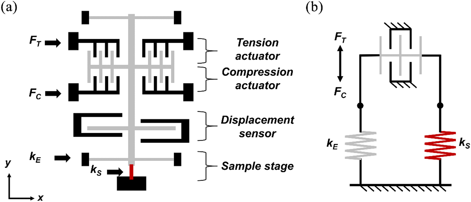
As schematically illustrated in Fig. 1(a), the tension–compression MEMS device consists of three parts: a tension electrostatic actuator, a compression electrostatic actuator and a displacement sensor. These structures are distributed on both sides of the moving shuttle, while the mechanical test system is suspended by several pairs of support beams. The sample stage is composed of a moving shuttle and a fixed block. By applying voltages on different actuators, the device can achieve tension or compression modes. The displacement of the actuator is measured using a differential capacitive sensor or SEM images. The symmetrical design of the structure ensures that the system has the same theoretical driving ability and displacement sensitivity in both tension and compression modes. This method, compared to the classical three-spring test system,39 allows for a wider measurement range by fully utilizing the displacement of the electrostatic actuator for sample testing.40Fig. 1(b) illustrates the lumped mechanical model of the test system used to analyze deformation compatibility and force distribution. When the system is in static equilibrium, the governing equations of the system are given as follows:| | | FS = ΔUS × kS = FE − UE × kE | (1c) |
where FE is the actuation force generated by the tension or compression actuator at the applied voltage V, replaced by FT and FC in Fig. 1. N, t and g are the number of combs, the gap between fingers, and the thickness of the device, respectively. ε is the dielectric constant. UE and ΔUS are the actuator displacement and sample deformation, respectively, which are the same in the load mode. FS is the force applied to the sample, kS and kE are the stiffness of the sample and the actuator, respectively.
 |
| | Fig. 1 Schematics of the structure (a) and lumped mechanical model (b) of the tension–compression MEMS device. | |
In practical tests, the actuation displacement of electrostatic actuators usually deviates from the prediction of eqn (1a) due to process errors and parasitic capacitance.41 Therefore, in order to accurately characterize the actuation force FE, experiments need to perform displacement characterization at different voltages under no-load conditions. The following formulas are used instead of eqn (1a):
where
a and
b are the parameters obtained after curve fitting. It should be noted that different from
eqn (1),
UE represents the displacement of the actuator under no-load conditions. Through
eqn (1) and (2), the force and displacement of the nanostructures under different voltages can be obtained. Combined with the morphology characteristics of the nanostructures, mechanical parameters such as Young's modulus, yield strength, and fracture strength under tension–compression mode can be further extracted.
Device design and fabrication
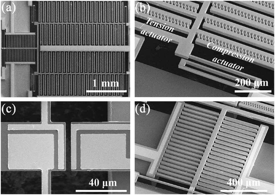
The SEM image of the tension–compression MEMS device is presented in Fig. 2(a). Different from the schematic diagram in Fig. 1(a), the tension actuator and compression actuator are located inside and outside of the moving shuttle, respectively, as shown in Fig. 2(b). This design method can effectively reduce the device area while ensuring the symmetry of the structure, which is essential for in situ testing. The support system of the device is composed of fixed–fixed beams, folded beams, and serpentine beams, which provide significant out-of-plane stiffness while maintaining low axial stiffness.40 The sample stage area consists of the moving shuttle, the fixed structure, and a four-probe electrical test structure designed for the subsequent tension–compression electromechanical testing, as shown in Fig. 2(c). Fig. 2(d) illustrates a differential capacitance sensor utilized in both tension and compression modes. The differential structure enhances the anti-noise ability of the capacitive sensor, ensuring a linear relationship between capacitance change and actuation displacement.42 The MEMS device was fabricated on a 4-inch silicon-on-insulator (SOI) wafer using a previously proposed compatible process.40,43 The single-crystal Si structural layer thickness is 30 μm and isolated from the substrate by a 0.5 μm-thick SiO2 layer. The metal electrodes consist of a 200 nm Au and 20 nm Ti bonding layer prepared by sputtering. The through-hole structure can be fabricated by this process, which is a necessary characterization for TEM testing.
 |
| | Fig. 2 SEM images of the MEMS device: (a) the overall view, (b) the tension and compression actuators, (c) the sample stage, (d) the differential capacitive sensor. | |
Test system setup
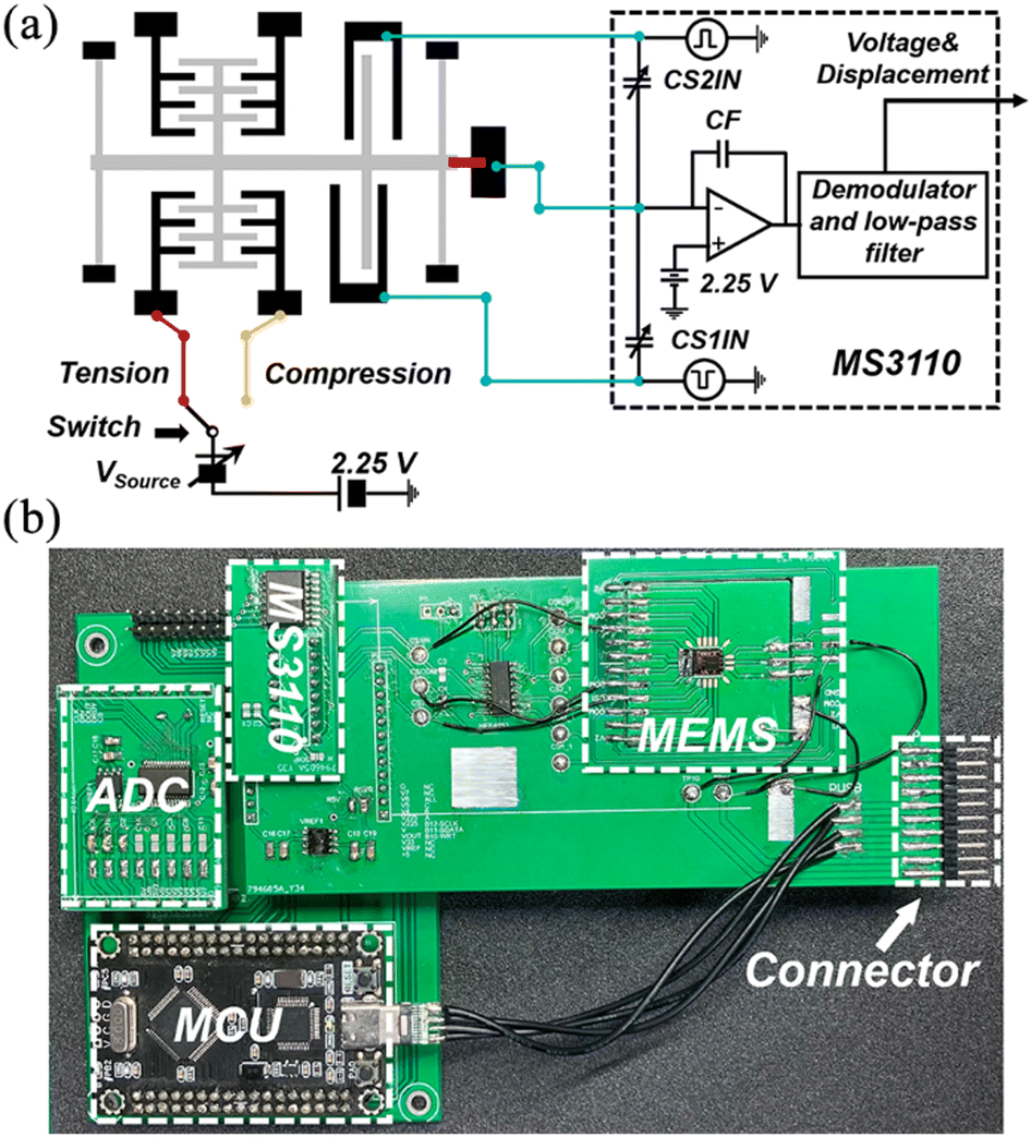
The setup of the test system based on the tension–compression MEMS device is shown in Fig. 3(a). The device uses a differential capacitive sensor structure, providing a theoretical sensitivity of S = 0.19 fF nm−1. The capacitance change was measured using a commercially capacitive readout chip36 (MS3110, Irvine Sensors). The two fixed plates of the differential capacitor are respectively connected to the CS1IN and CS2IN ports of MS3110, while the moving shuttle is connected to the COM port. This configuration makes the device exhibit opposite trends in capacitance changes under tension and compression modes without the need for circuit reconnection. The selection of the mechanical load mode is realized by simple switch equipment, connected to an adjustable voltage source for load control. For tension–compression fatigue testing, this switch can be replaced by a relay with a signal generator for frequency control.
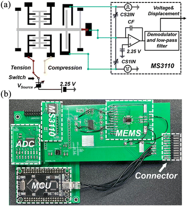 |
| | Fig. 3 (a) The schematic of the test system setup based on the MEMS device. (b) The PCB contains the wire-bonded MEMS device and capacitive readout circuit. | |
Fig. 3(b) shows the assembled PCB test board designed for the SEM environment, which consists of three modules: microcontroller unit (MCU), analog-to-digital converter (ADC), and MEMS development board (ESI†). This module design ensures compatibility with various types of MEMS devices. The wire-bonded MEMS device and MS3110 chip are integrated into the MEMS development board to reduce the noise.34 The ADC chip is responsible for collecting the output signal from the MS3110, while the MCU controls both the ADC and MS3110 chip. The test system is controlled by an external computer and voltage source through the connector and flange. For TEM environments, similar functionalities can be achieved by utilizing a customized sample holder44 for electrical connections.
Results and discussion
Device characterization
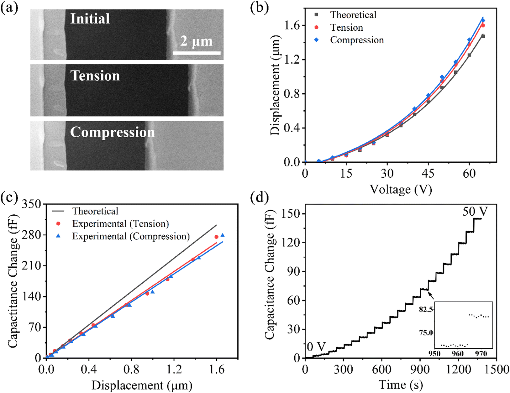
To evaluate the performance of the tension–compression MEMS device, we performed tests without samples. The DC source was applied to the actuators through the flange, and the change of the sample stage gap was observed using SEM. Fig. 4(a) shows the variation of the sample stage gap in the initial, tension, and compression states. The symmetrical structural design results in identical theoretical actuation displacements and capacitance changes in tension and compression modes. The tension and compression actuation displacements at specific voltages are relatively consistent, as shown in Fig. 4(b). Meanwhile, the capacitance changes in both modes show a linear relationship with displacement (Fig. 4(c)). The deviations between theoretical and experimental results are primarily attributed to process errors and parasitic capacitance,41 which can be mitigated through the use of a calibration constant.45Fig. 4(d) shows the stability test results of the capacitive sensor in a single mode. By applying a stepped voltage to the actuator, the obtained capacitance changes exhibit a stable tracking characteristic. The fluctuation of capacitance change at a certain voltage is about 0.64 fF (inset in Fig. 4(d)), indicating high stability.
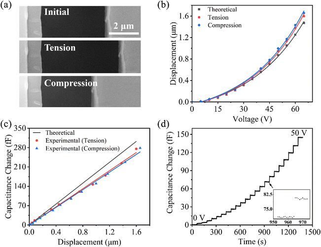 |
| | Fig. 4 (a) SEM images of sample stage gap changes in the initial, tension, and compression states. (b) Calibration of the tension and compression actuators. (c) Calibration of capacitive sensors in tension and compression modes. (d) Stability testing of the capacitive sensor. | |
Fabrication of Pt and C nanostructures based on FIB
The utilization of FIB nanofabrication technology offers a flexible and convenient approach to achieve complex geometrical architectures.46 This technology makes architectural design across a wide range of length scales possible. The fabrication principle is based on the interaction of an electron/ion beam with a precursor material to form a deposited product. The position and size of the product can be precisely controlled by the pattern generator. Moreover, Pt and C-based nanostructures created through FIB-induced deposition (IBID) have found extensive applications in various fields such as TEM sample preparation,47 structure fixation,48 and 3D nanoprinting.49 Therefore, the experiment carried out tests on nanostructures composed of these two materials to gain insights into the in situ nanofabrication techniques.
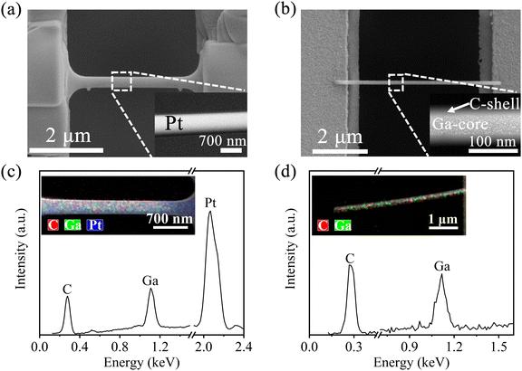
The fabrication process for Pt nanopillars is similar to the TEM sample preparation.50 First, a rectangular Pt block with a thickness of approximately 0.5 μm was deposited using a Ga+ ion beam with an accelerating voltage of 30 kV and a beam current of 80 pA. Next, the Pt block was extracted, and the substrate was fully etched by rotating the nanomanipulator and employing FIB milling. Finally, the Pt block was transferred to the sample stage and cut into a dog-bone shape, as shown in Fig. 5(a). The marks of the Pt nanopillar provide a better view of the amount of sample deformation. On the other hand, the C nanowire was directly fabricated under a Ga+ ion beam with an accelerating voltage of 16 kV and beam current of 1.1 pA without the use of a nanomanipulator. The ion beam is incident perpendicular to the target area, and phenanthrene is injected into the FIB chamber using a gas injection system (GIS). The ion beam, controlled by a computer-aided design (CAD) program,49 interacts with the precursor for deposition to form a suspended C nanowire (Fig. 5(b)). The different preparation methods of the two material systems resulted in distinct nanostructural features, as revealed by scanning transmission electron microscopy (STEM). The Pt nanopillar exhibits a substantial structure. Conversely, the C nanowire features an amorphous C shell in the structure, encapsulating a core with small precipitates of amorphous gallium.51Fig. 5(c) and (d) show the energy spectrum (EDS) analysis and elemental distributions of the two materials, revealing the nature of the hybrid.
 |
| | Fig. 5 SEM image of the (a) Pt nanopillar and (b) C nanowire fabricated by FIB. The insets are STEM images of the Pt nanopillar and C nanowire. EDS analysis of the (c) Pt nanopillar and (d) C nanowire. | |
Tension test of the Pt nanopillar and C nanowire
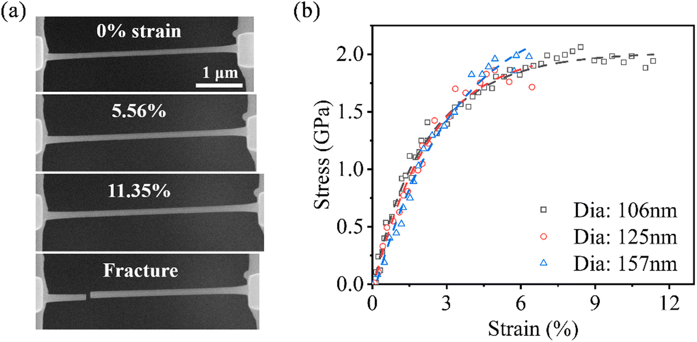
To validate the effectiveness of the device, we carried out uniaxial tensile tests on the Pt nanopillars and C nanowires. Both nanostructures were fixed by Pt blocks fabricated through electron/ion beam induced deposition (EBID/IBID). Switching the system to tension testing mode, a continuous DC voltage was applied to the tensile actuator to drive the sample stage. Fig. 6(a) shows the deformation behavior of the Pt nanopillar during the tension test, with the increasing spacing of the marked points indicating the progression of deformation. The stress–strain curves of the Pt nanopillars are shown in Fig. 6(b) and categorized by the width of the smallest dimension in the geometry, indicating that obvious plastic deformation during testing. The obtained Young's modulus in the linear interval of the curves ranged from 62.08–77.07 GPa, with an average value of 70.06 GPa, which is in agreement with previous reports.52,53 The maximum fracture strain and stress of the Pt nanopillars reached 15.05% and 3.69 GPa, respectively, and no significant size-dependent phenomenon was observed in the tests. Similarly, the deformation behavior and stress–strain curves of the C nanowires in the tension test are shown in Fig. 7. The Young's modulus ranged from 53.09 to 64.39 GPa with an average value of 58.32 GPa, which is consistent with previous reports.54,55 Notably, the nanowires with a diameter of 106 nm exhibited the most excellent mechanical properties in terms of Young's modulus (64.39 GPa), fracture strength (2.06 GPa), and maximum tensile strain (11.35%), indicating a size-dependent phenomenon. Both Pt and C nanostructures exhibited excellent ductility and fracture strength in the tension tests, showcasing promising applications for future nanomechanical components.
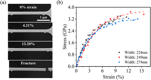 |
| | Fig. 6 Sequential SEM images (a) and strain–stress curves (b) of the Pt nanopillar during tension to fracture. | |
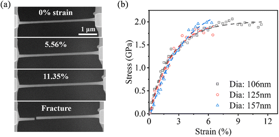 |
| | Fig. 7 Sequential SEM images (a) and strain–stress curves (b) of the C nanowire during tension to fracture. | |
Compression test of the Pt nanopillar and C nanowire
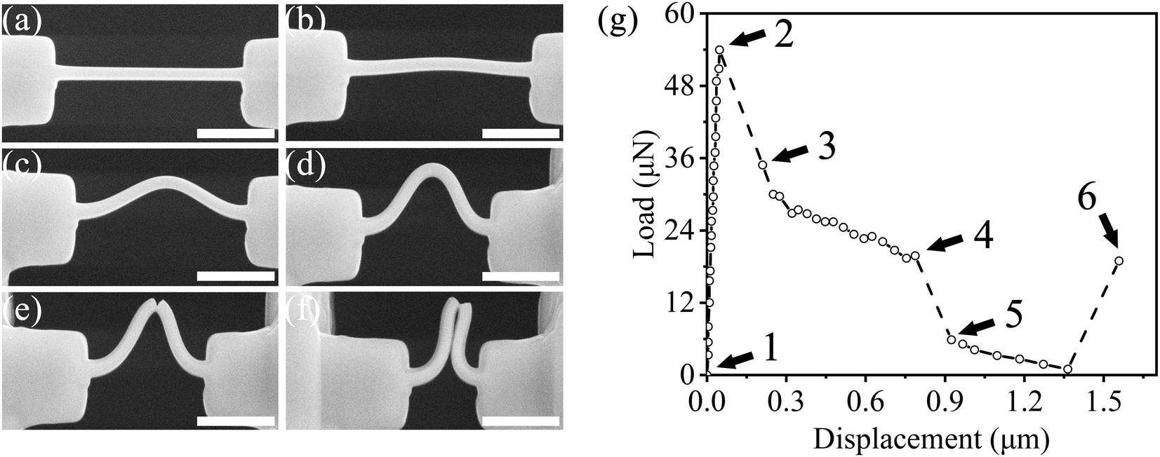
The Pt nanopillar for compression testing was fabricated using the same method as the tension samples. However, it should be noted that the nanopillar used for compression testing did not have marks and was designed in a rectangular shape instead of a dog-bone shape. The geometry was chosen for two reasons. Firstly, the smaller size of the compressed sample reduces the displacement error caused by direct observation less than 1.5 nm, which meets the test requirements. Secondly, the rectangular structure makes it possible to extract mechanical parameters during compression deformation by the Euler buckling model.56 As the compressive displacement increases, the nanopillar undergoes a series of states. Starting from the initial state (Fig. 8(a)), the nanopillar gradually reaches the limit of the elastic state (Fig. 8(b)). A small displacement increment beyond the elastic limit can cause the nanopillar to buckle (Fig. 8(c)), and the degree of buckling increases gradually (Fig. 8(d)). Cracks begin to appear in the nanopillar (Fig. 8(e)), deepening as the compressive displacement continues. Finally, the broken segments of the nanopillar stick together (Fig. 8(f)), leading to a re-increase in the applied mechanical loads. The variation of the applied load with the axial displacement of the nanopillar is shown in Fig. 8(g). Since the stress and strain are not uniform across the sample in the compressed state, the Young's modulus is extracted from the linear portion of the mechanical curve using Euler's formula:where Pcr is the critical buckling force acquired by the compression test, E is the Young's modulus, I is the moment of inertia of the Pt nanopillar, and Le is the effective length equal to half of the actual length in this experiment. The Young's modulus of the Pt nanopillar obtained under the compression test is 68.81 GPa, which is consistent with the results from the tension test. The yield strength is determined to be 912 MPa.
 |
| | Fig. 8 (a)–(f) A series of SEM images of the Pt nanopillar during the compression test. (g) The load–displacement curve of the Pt nanopillar. Points 1–6 mark the load–displacement characteristics of the Pt nanopillar with the deformation state in images (a)–(f), respectively. Scale bar: 1 μm. | |
The C nanowire for compression testing was fabricated using the same method as the tension testing, and the deformation behavior is illustrated in Fig. 9(a). Since the deformation of each part of the nanowire was not uniform under compression, the strain at the bending part was selected for comparison in the experiment. The strain ε was calculated according to the formula:26
where
r is the radius of the nanowire and
ρ is the curvature radius of the inner edge of the nanowire. The C nanowires exhibited a bending strain of up to 25.47% during compression, without experiencing fracture, which is significantly higher than that observed in the tension experiments (11.35%). The 3D twisting deformation of the C nanowire results in a scattered curve during compression testing (
Fig. 9(b)). The apparent tension–compression asymmetry may be attributed to the different sensitivities of defects and deformation mechanisms under tension
versus compression. Specifically, the tension load tends to cause premature fracture at low stresses by causing the defects to initially form cracks and accelerating their expansion. In contrast, defects tend to close under compression load, allowing the nanomaterial to withstand greater deformation.
20 The excellent flexibility exhibited by the C nanowire under compression loads provides promising applications for nano-strain engineering.
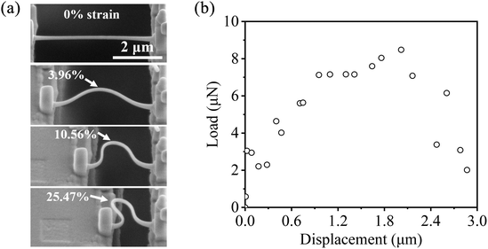 |
| | Fig. 9 (a) A series of SEM images of the C nanowire during the compression test. (b) The load–displacement curve of the C nanowire. | |
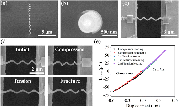
Tension–compression test of a C nanospring
The tension–compression continuous test capability of the device was verified using a C nanospring fabricated through FIB 3D nanoprinting. The designed growth paths were imported into the pattern controller of the FIB, and growth was carried out at an accelerating voltage of 16 kV and a beam current of 1.1 pA. The front and top-view SEM images of the C nanospring are shown in Fig. 10(a) and (b), respectively, displaying a standard 3D helical structure. A nanomanipulator was used to connect and extract the nanospring. The angle and position of the nanomanipulator were adjusted to align the nanospring axial direction with the device's actuation direction, and a uniform area of the nanospring was placed on the test stage. EBID Pt blocks (5 kV, 0.34 nA) were used to fix both ends of the spring, as illustrated in Fig. 10(c). Five continuous loading–unloading tests were performed on the C nanospring in tension–compression mode. Fig. 10(d) depicts the images of the nanospring in the initial state, at the compressive limit, at the tension limit and following fracture, which indicates the non-uniform deformation in compression as compared to tension. The change in mechanical behavior caused by this non-uniformity is also observed in the load–displacement curve shown in Fig. 10(e). It can be observed that the loading and unloading curves under the compression test deviate slightly, while in the tension test, they almost coincide. Moreover, the linearity of the mechanical curves in the tensile test is much better than that in the compression test. The intrinsic properties of the nanospring can be evaluated by the spring constant, which is obtained by solving the slope of the load–displacement curve (Fig. 10(e)). The average spring constants in the tension and compression modes are 143.53 N m−1 and 120.81 N m−1, respectively. The experimental results highlight an unexplored regime of intrinsic tension–compression asymmetry in nanostructures. In addition, the non-traditional design of nanosprings relies on advanced nanofabrication technology. Mixed helical structures with different diameters have been reported,57 and analysis of the intrinsic mechanical properties may require the assistance of finite element simulation.
 |
| | Fig. 10 The front (a) and top view (b) SEM images of the C nanospring fabricated by FIB 3D nanoprinting. (c) SEM image of the nanospring transferred and fixed by a nanomanipulator and EBID. (d) A series of SEM images of the C nanowire during the tension–compression test. (e) The load–displacement curve of the C nanospring. | |
Conclusion
This paper presents a MEMS device that enables in situ quantitative tension–compression mechanical testing of nanostructures. The device consists of tension and compression electrostatic actuators, a differential capacitance sensor, and an external control circuit for the measurement of mechanical properties. Systematic investigations were carried out to analyze the mechanical behavior of Pt nanopillars and C nanowires fabricated by FIB under tension and compression loads. The stress–strain curves obtained from the tension tests demonstrated clear plastic characteristics for both Pt nanopillars and C nanowires. The Pt nanopillars exhibited a maximum fracture stress of 3.69 GPa and a maximum strain of 15.05%. Similarly, the C nanowires displayed a maximum fracture stress of 2.06 GPa and a maximum strain of 11.35%. In the compression test, the Pt nanopillar exhibited in-plane buckling behavior, and the obtained Young's modulus was consistent with the tensile test. On the other hand, the C nanowire exhibited 3D twisting behavior, with a maximum bending strain of 25.47%, significantly higher than that observed in tension tests. Furthermore, tension–compression asymmetry was observed in the C nanospring fabricated by FIB 3D nanoprinting. The loading–unloading mechanical curves in the compression test deviated from linearity and exhibited inferior linearity compared to the tension test, where the curves overlapped and showed high linearity. These results show that the developed device possesses excellent tension–compression mechanical testing capability, which can provide an important evaluation basis for the fabrication and design of nanostructures.
Author contributions
The whole work was performed under the supervision of Meng Nie and Kuibo Yin. Yuheng Huang and Kuibo Yin performed the MEMS design. Yuheng Huang, Binghui Li, and Bozhi Wu performed sample preparation and measurement testing. Anqi Zheng performed the TEM characterization. Litao Sun provided experimental and equipment support. All authors performed the data analysis. All authors read and contributed to the manuscript.
Conflicts of interest
There are no conflicts to declare.
Acknowledgements
The authors acknowledge the funding provided by the National Natural Science Foundation of China (No. 62274031, 12174050, and 12234005), the Jiangsu Provincial Natural Science Foundation of China (Grant No. BK20201268, BK20222007, and BK20231411), the key research and development program of Jiangsu Province (BE2021007-2), and the Fundamental Research Funds for the Central Universities.
Notes and references
- Y. Zhu, Q. Qin, F. Xu, F. Fan, Y. Ding, T. Zhang, B. J. Wiley and Z. L. Wang, Phys. Rev. B: Condens. Matter Mater. Phys., 2012, 85, 045443 CrossRef.
- M. Chen, L. Petho, A. S. Sologubenko, H. Ma, J. Michler, R. Spolenak and J. M. Wheeler, Nat. Commun., 2020, 11, 2681 CrossRef CAS PubMed.
- T.-H. Chang, G. Cheng, C. Li and Y. Zhu, Extreme Mech. Lett., 2016, 8, 177–183 CrossRef.
- S. Narayanan, G. Cheng, Z. Zeng, Y. Zhu and T. Zhu, Nano Lett., 2015, 15, 4037–4044 CrossRef CAS PubMed.
- Y. Wang, L. Tian, M. Li and Z. Shan, J. Mater. Sci. Technol., 2023, 166, 106–112 CrossRef.
- G. Cheng, T. H. Chang, Q. Qin, H. Huang and Y. Zhu, Nano Lett., 2014, 14, 754–758 CrossRef CAS PubMed.
- C. Cao, M. Daly, B. Chen, J. Y. Howe, C. V. Singh, T. Filleter and Y. Sun, Nano Lett., 2015, 15, 6528–6534 CrossRef CAS PubMed.
- R. Ramachandramoorthy, W. Gao, R. Bernal and H. Espinosa, Nano Lett., 2016, 16, 255–263 CrossRef CAS PubMed.
- C. Dang, J.-P. Chou, B. Dai, C.-T. Chou, Y. Yang, R. Fan, W. Lin, F. Meng, A. Hu, J. Zhu, J. Han, A. M. Minor, J. Li and Y. Lu, Science, 2021, 371, 76–78 CrossRef CAS PubMed.
- H. Zhang, J. Tersoff, S. Xu, H. Chen, Q. Zhang, K. Zhang, Y. Yang, C.-S. Lee, K.-N. Tu and J. Li, Sci. Adv., 2016, 2, e1501382 CrossRef PubMed.
- S. Fan, X. Feng, Y. Han, Z. Fan and Y. Lu, Nanoscale Horiz., 2019, 4, 781–788 RSC.
- M. Amjadi, A. Pichitpajongkit, S. Lee, S. Ryu and I. Park, ACS Nano, 2014, 8, 5154–5163 CrossRef CAS PubMed.
- C. Dagdeviren, P. Joe, O. L. Tuzman, K. I. Park, K. J. Lee, Y. Shi, Y. G. Huang and J. A. Rogers, Extreme Mech. Lett., 2016, 9, 269–281 CrossRef.
- J. U. Surjadi, L. Gao, H. Du, X. Li, X. Xiong, N. X. Fang and Y. Lu, Adv. Eng. Mater., 2019, 21, 1800864 CrossRef CAS.
- J. Bauer, A. Schroer, R. Schwaiger and O. Kraft, Nat. Mater., 2016, 15, 438–443 CrossRef CAS PubMed.
- B. B. Lewis, B. A. Mound, B. Srijanto, J. D. Fowlkes, G. M. Pharr and P. D. Rack, Nanoscale, 2017, 9, 16349–16356 RSC.
- A. Xu, M. Saleh and D. Bhattacharyya, Composites, Part B, 2020, 186, 107823 CrossRef CAS.
- M. F. Pantano and I. Kuljanishvili, Nano Express, 2020, 1, 022001 CrossRef.
- A. B. Hagen, B. D. Snartland and C. Thaulow, Acta Mater., 2017, 129, 398–407 CrossRef CAS.
- Y. Wang, J. Ding, Z. Fan, L. Tian, M. Li, H. Lu, Y. Zhang, E. Ma, J. Li and Z. Shan, Nat. Mater., 2021, 20, 1371–1377 CrossRef CAS PubMed.
- H. Jeon, S. Lee and J.-Y. Kim, Acta Mater., 2020, 199, 340–351 CrossRef CAS.
- D. Zhang, J.-M. Breguet, R. Clavel, V. Sivakov, S. Christiansen and J. Michler, J. Microelectromech. Syst., 2010, 19, 663–674 Search PubMed.
- C. Zhang, D. G. Kvashnin, L. Bourgeois, J. F. S. Fernando, K. Firestein, P. B. Sorokin, N. Fukata and D. Golberg, Nano Lett., 2018, 18, 7238–7246 CrossRef CAS PubMed.
- C. H. Lin, H. Ni, X. Wang, M. Chang, Y. J. Chao, J. R. Deka and X. Li, Small, 2010, 6, 927–931 CrossRef CAS PubMed.
- S. Lee, J. Im, Y. Yoo, E. Bitzek, D. Kiener, G. Richter, B. Kim and S. H. Oh, Nat. Commun., 2014, 5, 3033 CrossRef PubMed.
- F. Liu, D.-M. Tang, H. Gan, X. Mo, J. Chen, S. Deng, N. Xu, Y. Bando and D. Golberg, ACS Nano, 2013, 7, 10112–10120 CrossRef CAS PubMed.
- D. M. Tang, C. L. Ren, M. S. Wang, X. Wei, N. Kawamoto, C. Liu, Y. Bando, M. Mitome, N. Fukata and D. Golberg, Nano Lett., 2012, 12, 1898–1904 CrossRef CAS PubMed.
- Y. B. Wang, L. F. Wang, H. J. Joyce, Q. Gao, X. Z. Liao, Y. W. Mai, H. H. Tan, J. Zou, S. P. Ringer, H. J. Gao and C. Jagadish, Adv. Mater., 2011, 23, 1356–1360 CrossRef CAS PubMed.
- T. Sumigawa, K. Byungwoon, Y. Mizuno, T. Morimura and T. Kitamura, Acta Mater., 2018, 153, 270–278 CrossRef CAS.
- Y. Yan, T. Sumigawa, X. Wang, W. Chen, F. Xuan and T. Kitamura, Int. J. Mech. Sci., 2020, 171, 105361 CrossRef.
- H. Zhang, C. Jiang and Y. Lu, Exp. Mech., 2016, 57, 495–500 CrossRef.
- J. Shin, G. Richter and D. S. Gianola, Mater. Des., 2020, 189, 108460 CrossRef.
- J. Qu and X. Liu, IEEE Sens. J., 2022, 22, 1827–1841 CAS.
- H. D. Espinosa, Y. Zhu and N. Moldovan, J. Microelectromech. Syst., 2007, 16, 1219–1231 Search PubMed.
- E. Hosseinian and O. N. Pierron, Nanoscale, 2013, 5, 12532–12541 RSC.
- S. Gupta and O. N. Pierron, Extreme Mech. Lett., 2016, 8, 167–176 CrossRef.
- M. Elhebeary and M. T. A. Saif, Extreme Mech. Lett., 2018, 23, 1–8 CrossRef.
- A. Barrios, S. Gupta, G. M. Castelluccio and O. N. Pierron, Nano Lett., 2018, 18, 2595–2602 CrossRef CAS PubMed.
- Y. Zhu, A. Corigliano and H. D. Espinosa, J. Micromech. Microeng., 2006, 16, 242–253 CrossRef CAS.
- Y. Huang, M. Nie, B. Wu, B. Li, K. Yin and L. Sun, Sens. Actuators, A, 2022, 347, 113953 CrossRef CAS.
- T. Tsuchiya, Y. Ura, K. Sugano and O. Tabata, J. Microelectromech. Syst., 2012, 21, 523–529 CAS.
- C. Li, G. Cheng, H. Wang and Y. Zhu, Exp. Mech., 2020, 60, 1005–1015 CrossRef.
-
Y. Huang, M. Nie, B. Li, K. Yin and L. Sun, Proceeding IEEE 36th International Conference on Micro Electro Mechanical Systems (MEMS), 2023, 771–774.
- R. A. Bernal, R. Ramachandramoorthy and H. D. Espinosa, Ultramicroscopy, 2015, 156, 23–28 CrossRef CAS PubMed.
- S. Gupta and O. N. Pierron, J. Microelectromech. Syst., 2017, 26, 1082–1092 CAS.
- P. Li, S. Chen, H. Dai, Z. Yang, Z. Chen, Y. Wang, Y. Chen, W. Peng, W. Shan and H. Duan, Nanoscale, 2021, 13, 1529–1565 RSC.
- J. Zhang, Y. Li, X. Li, Y. Zhai, Q. Zhang, D. Ma, S. Mao, Q. Deng, Z. Li, X. Li, X. Wang, Y. Liu, Z. Zhang and X. Han, Nat. Commun., 2021, 12, 2218 CrossRef CAS PubMed.
- Q. Qin, F. Xu, Y. Cao, P. I. Ro and Y. Zhu, Small, 2012, 8, 2571–2576 CrossRef CAS PubMed.
- R. Winkler, J. D. Fowlkes, P. D. Rack and H. Plank, J. Appl. Phys., 2019, 125, 210901 CrossRef.
- N. S. Rajput, K. Sloyan, D. H. Anjum, M. Chiesa and A. A. Ghaferi, Ultramicroscopy, 2022, 235, 113496 CrossRef CAS PubMed.
- M. Esposito, V. Tasco, F. Todisco, M. Cuscuna, A. Benedetti, M. Scuderi, G. Nicotra and A. Passaseo, Nano Lett., 2016, 16, 5823–5828 CrossRef CAS PubMed.
- I. Utke, J. Michler, R. Winkler and H. Plank, Micromachines, 2020, 11, 397 CrossRef PubMed.
- A. Reiser, L. Koch, K. A. Dunn, T. Matsuura, F. Iwata, O. Fogel, Z. Kotler, N. Zhou, K. Charipar, A. Pique, P. Rohner, D. Poulikakos, S. Lee, S. K. Seol, I. Utke, C. van Nisselroy, T. Zambelli, J. M. Wheeler and R. Spolenak, Adv. Funct. Mater., 2020, 30, 1910491 CrossRef CAS PubMed.
- M. Kiuchi, S. Matsui and Y. Isono, J. Microelectromech. Syst., 2007, 16, 191–201 CAS.
- S. Okada, T. Mukawa, R. Kobayashi, M. Ishida, Y. Ochiai, T. Kaito, S. Matsui and J. I. Fujita, Jpn. J. Appl. Phys., 2006, 45, 5556–5559 CrossRef CAS.
- F. Xu, Q. Q. Qin, A. Mishra, Y. Gu and Y. Zhu, Nano Res., 2010, 3, 271–280 CrossRef CAS.
- C. Fang, Q. Chai, Y. Chen, Y. Xing and Z. Zhou, Precis. Eng., 2022, 77, 241–250 CrossRef.
|
| This journal is © The Royal Society of Chemistry 2024 |
Click here to see how this site uses Cookies. View our privacy policy here. 
 *,
Binghui
Li
,
Anqi
Zheng
,
Bozhi
Wu
,
Litao
Sun
*,
Binghui
Li
,
Anqi
Zheng
,
Bozhi
Wu
,
Litao
Sun