
 Open Access Article
 This Open Access Article is licensed under a
 Creative Commons Attribution 3.0 Unported Licence
Phonon vortices at heavy impurities in two-dimensional materials†
De-Liang
Bao
a,
Mingquan
Xu
 b,
Ao-Wen
Li
b,
Gang
Su
bc,
Wu
Zhou
b and
Sokrates T.
Pantelides
*ad
b,
Ao-Wen
Li
b,
Gang
Su
bc,
Wu
Zhou
b and
Sokrates T.
Pantelides
*ad
aDepartment of Physics and Astronomy, Vanderbilt University, Nashville, Tennessee 37235, USA. E-mail: pantelides@vanderbilt.edu
bSchool of Physical Sciences and CAS Key Laboratory of Vacuum Physics, University of the Chinese Academy of Sciences, Beijing 100049, P. R. China
cKavli Institute for Theoretical Sciences, University of the Chinese Academy of Sciences, Beijing, P. R. China
dDepartment of Electrical and Computer Engineering, Vanderbilt University, Nashville, Tennessee 37235, USA
First published on 7th December 2023
Abstract
The advent of monochromated electron energy-loss spectroscopy has enabled atomic-resolution vibrational spectroscopy, which triggered interest in spatially localized or quasi-localized vibrational modes in materials. Here we report the discovery of phonon vortices at heavy impurities in two-dimensional materials. We use density-functional-theory calculations for two configurations of Si impurities in graphene, Si–C3 and Si–C4, to examine atom-projected phonon densities of states and display the atomic-displacement patterns for select modes that are dominated by impurity displacements. The vortices are driven by large displacements of the impurities, and reflect local symmetries. Similar vortices are found at phosphorus impurities in hexagonal boron nitride, suggesting that they may be a feature of heavy impurities in crystalline materials. Phonon vortices at defects are expected to play a role in thermal conductivity and other properties.
New conceptsThe paper introduces and documents theoretically the new concept of “phonon vortices” that can form at heavy impurities in two-dimensional materials. Though impurities and other point defects in materials have long been studied for their structural, electronic, optical, magnetic, and other properties and for their impact on macroscopic properties by both experimentalists and theorists, their vibrational properties have received little attention. The main deterrent has been the lack of experimental techniques that can probe vibrational properties with sufficient spatial resolution. In recent years, the advent of monochromated, aberration-corrected scanning transmission electron microscopes has enabled atomic-resolution vibrational electron-energy-loss spectroscopy (vEELS) with high energy resolution. Many high-profile studies have been published. Here, the discovery of vortices is documented with density-functional-theory calculations for heavy impurities like Si in graphene and phosphorus in hexagonal BN. Vortices feature circular paterns of vibrating atoms that reflect the local symmetry and connect to a pristine-phonon wave. The key driver for vortex formation is the large heavy-atom vibrational displacements at a characteristic frequency. Next-generation microscopes are likely to be able to produce maps of phonon vortices. They are expected to exist in other materials, including possibly bulk solids, and to impact thermal properties such as thermal conductivity. |
Defects, namely inhomogeneities in the atomic arrangement of materials, are ubiquitous, making their engineering essential to tune macroscopic functional properties. Extensive fundamental research has been conducted on defects, focusing on topics such as electronic energy levels in semiconductor band gaps,1 defect formation and migration energies,2,3 optical and magnetic properties,4 catalytic effects,5 and defect-mediated reliability issues in electronic, optoelectronic, and electrical devices.6–8 Nevertheless, the vibrational properties of defects have received limited attention even though they are equally fundamental and play a role in thermal conduction,9 phase transitions,10 structural stability,11 infrared absorption12 and dielectric response,13 nanofluid transport,14 and superconductivity through electron–phonon coupling.15 Conventional treatments of phonons in defective materials typically focus on phonon scattering from defects,16 which affects parameters such as phonon lifetimes, mean free paths, and phonon–phonon coupling. Unusual phenomena have also been found to occur at defects, such as the stabilization of carbon–hydrogen bonds on graphene by an in-plane sonic wave17 and the use of acoustic-phonon waves to probe the location of point defects.18
Conventionally, experimental investigations of phonons in materials have been based on optical and neutron-scattering techniques with limited spatial resolution. Recent advances in experimental techniques, however, particularly the development of monochromated electron energy-loss spectroscopy (EELS) in scanning transmission electron microscopes (STEM), have revolutionized this field.19 These breakthroughs paved the way for phonon spectroscopy with exceptional atomic-scale spatial resolution and meV-scale energy resolution.20 Atomic-scale phonon spectroscopy has been carried out at point defects,21 interfaces,22 stacking faults,23 grain boundaries,24 and even with chemical-bond sensitivity.25 The spatially resolved spectra feature peaks at energies that are distinct from those of the pure material, arising from different atomic masses and local atomic arrangements.21,25 Theoretical calculations based on density-functional theory (DFT) have been an equal partner in the enterprise by offering predictions of such energies and going beyond the reach of experiments to describe the atomic displacements and the extent of localization, which depends on whether the new energies lie within the continuum or within energy gaps in perfect-crystal phonon dispersions.21–25
In this paper, we employ DFT calculations and unveil a particularly notable feature of the vibrational properties of point defects in two-dimensional materials, namely the existence of vibrational modes with atomic displacements that form circular patterns around a heavy impurity in the shape of a vortex. We call such circular vibrational patterns “phonon vortices”. The energies (frequencies) of these modes do not necessarily lie in an energy gap in the perfect-crystal phonon dispersion, even if such a gap exists, whereby the corresponding vortices are connected to perfect-crystal phonon waves (such defect-induced quasi-localized states within the band continua are known to be induced by defects in the electron energy bands and are referred to as resonances26). Thus, defect-induced phonon vortices within the continua of perfect-crystal phonon dispersion are analogs of vortices that form when flowing water runs into an obstacle, but the “obstacle” here, namely a heavy impurity atom, is actually vibrating with a relatively large displacement. More specifically, we report results for impurities in graphene and two-dimensional (2D) hexagonal boron nitride (h-BN). In graphene, we focus on Si impurities as prototype systems because Si is 2.3 times as heavy as C and is known to form two point defects with distinct bonding configurations, namely Si–C3 (a Si atom replacing a single C atom) and Si–C4 (a Si atom replacing two nearest-neighbor C atoms),27 shown in schematics in Fig. 1a. We follow up on the findings in ref. 25, which tracked the atom-by-atom vibrational EELS (vEELS) response at these two Si bonding configurations. The corresponding DFT calculations of atom-projected phonon density of states (PhDOS) successfully reproduce the vibrational features in measured vEELS and provide detailed analysis of the origin and shifts of the spectral peaks. The STEM/EELS energy resolution is not currently sufficient to map the vibrational patterns of individual frequencies, allowing only averages over a small range of frequencies, but future mapping of vortices remains a possibility. Calculations of phonon vortices in h-BN are also reported, but calculations in 2D materials with multiple atomic planes or bulk crystals are still prohibitively expensive. Phonon vortices at impurities are likely to impact phonon-impurity scattering and thus thermal properties such as a thermal conductance. For the same reason, even slight intermixing at interfaces may impact thermal conductivity.
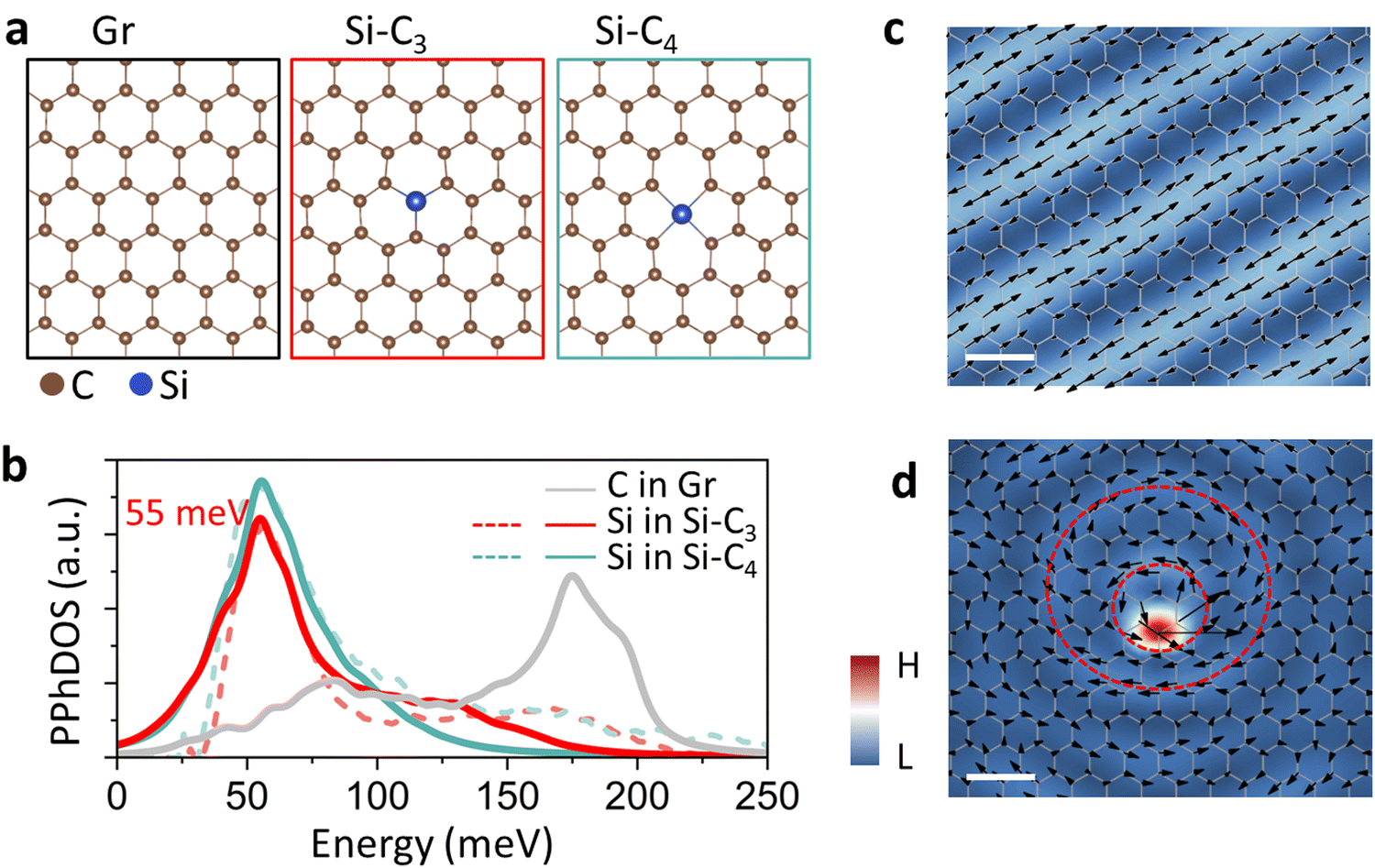 | ||
| Fig. 1 Phonons in intrinsic graphene and at defects. (a) Atomic schematics of intrinsic graphene (left), substitutional Si in graphene, Si–C3 (middle), and Si–C4, where the Si sits in a divacancy and therefore has four nearest C atoms (right). (b) Calculated PPhDOS on Si in Si–C3 and (red curve) and Si–C4 (cyan curve) compared with corresponding experimental vibrational EELS spectra extracted from the Si impurity25 (dashed curves). Calculated and measured spectra are normalized at the main-peak height. The gray curve is the PPhDOS on C atoms in pristine graphene. (c) Map of atomic displacements of a typical phonon mode of intrinsic graphene at an energy of 39 meV. This frequency is selected because of its suitability for visualization within a suitable range. (d) Atomic-displacement map of the vortex phonon mode of Si–C3 at the energy of 55 meV (peak energy in panel (b)). In the maps shown in (c) and (d), the arrows represent the in-plane components of atomic displacements and the colors correspond to their amplitudes. Scale bars: 0.5 nm. | ||
Graphene, a 2D honeycomb carbon network (Fig. 1a, left), has recently served as an ideal platform for studying phonons using monochromated vibrational EELS.21,25 With a relatively large broadening of the eigenstates, the phonon density of states (PhDOS) of graphene features two primary peaks. The lower-energy peak at ∼83 meV derives mostly from acoustic modes, while the higher-energy peak at ∼175 meV derives from optical modes.25 As expected, the projected PhDOS (PPhDOS) on a single C atom (gray in Fig. 1b) looks essentially identical as the total PhDOS.21
We examine phonons in graphene in the presence of the Si–C3 and Si–C4 defects that are depicted schematically in Fig. 1a. In both cases, the PPhDOS on Si (red and green curves in Fig. 1b) shows that a low-energy peak at ∼55 meV is induced while the optical peak effectively vanishes. These PPhDOSs on Si in Si–C3 and Si–C4 have been validated by atomically-resolved vEELS experiments.21,25 We attribute the distinct PPhDOS behavior of Si to the heavier mass of Si. In the acoustic region, the C atoms move collectively along the direction of the atomic displacements. The heavier Si vibrates intensely at a relatively low energy, according to the harmonic oscillator formula  , where ω is the frequency of vibration, k is an effective spring constant, and m is the Si-atom mass. The disappearance of the optical peak at 175 meV in the PPhDOS of Si is also caused by the Si-atom heavy mass. Si atoms simply cannot vibrate at such high frequencies. Recall that for perfect-crystal SiC, the phonon energies are no higher than 125 meV28 while in crystalline Si they only range to 65 meV.29
Given the notable distinctions in the PPhDOS on Si and on C in pristine graphene, the investigation of atomic displacements around defects becomes particularly intriguing. Fig. 1c depicts the atomic-displacement map of an individual phonon mode of pristine graphene at 39 meV, displaying a linear pattern with a periodicity corresponding to the wavelength. In contrast, the atomic-displacement map of Si–C3 around the first primary peak at ∼55 meV shows a remarkably different pattern (Fig. 1d). First, the color map, representing the atomic-displacement amplitude, indicates a very high intensity at the Si impurity, with observable intensity also present at the neighboring C atoms, suggesting that it is an impurity-dominated resonant phonon mode.30 Second, the color map shows that the local atomic displacements form circular features around the Si atom and dispersive strips radiating away from the Si. We have inserted two red dashed circles to highlight the dominant circular features. The inner circle passes very near the Si impurity, while the outer circle surrounds the inner one. The arrows depicted on the red circles represent a vortex behavior. The motion of the atoms is back and forth, in concert, in the direction of the little arrows.
To explore the formation mechanism of the phonon vortex, we reproduced the vortex in Fig. 1d using a larger computational supercell (Fig. 2a) and sandwiched it between two side panels showcasing the atomic displacements of the pristine-graphene mode closest to the energy at which the vortex forms. The intentionally placed gaps between the middle and side panels indicate that the connection to the pristine-graphene mode is likely to occur further out (see discussion later in the paper). In the middle panel, beyond the two inner vortices (red dashed circles in Fig. 2a), there are bending curves (yellow dashed curves in Fig. 2a). Upon closer examination, it becomes evident that the yellow dashed curves in the middle panel align remarkably well with the yellow dashed curves in the left and right panels. This alignment strongly suggests that the yellow dashed curves correspond to distorted phonon waves in intrinsic graphene. Recalling that the PPhDOS on Si of the Si–C3 defect only shows a primary peak in the acoustic-phonon regime of graphene, the formation of a phonon vortex in Si–C3 arises from the coupling between Si-atom vibrations and the pristine-graphene Bloch acoustic-phonon at the same energy. To illustrate the mechanism, we draw an analogy between the flow of water around an obstacle (right inset in Fig. 2b) and the formation of the phonon vortex. When water waves, analogous to phonon waves, propagate around an obstacle (representing the defect), a vortex forms around the obstacle (defect). Accordingly, the vortices depend on the obstacle's shape and size (analogous to the defect's local symmetry and mass, respectively), as well as the properties of the flowing liquid (representing the host material).
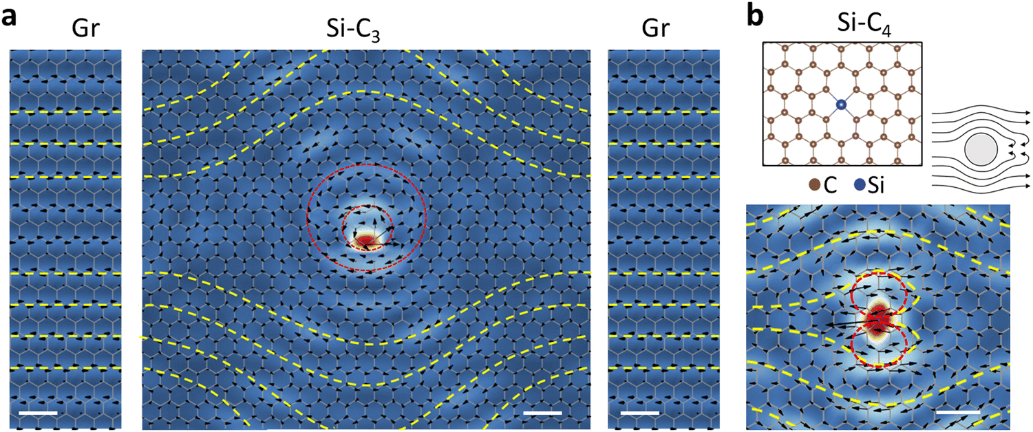 | ||
| Fig. 2 Phonon vortices at defects. (a) A larger view of the Si–C3 vortex of Fig. 1d, obtained with a four-times-larger supercell (see Methods), sandwiched between side panels depicting the atomic displacements of a pristine-graphene mode at ∼57 meV, which is closest to the energy of the PPhDOS on Si in the larger supercell. The gaps between the panels indicate that the overall connection is likely to happen farther away from the vortex. (b) A phonon-vortex map of Si–C4 at 56 meV. Top inset: Atomic configuration of Si–C4 and illustration of water flowing around an obstacle. | ||
The morphology of phonon vortices relates to the local symmetry of defects. In Si–C4, the Si impurity is chemically bonded to four surrounding C atoms. We again observe phonon vortices in Si–C4 at the phonon modes with frequencies around the first primary peak of the PPhDOS on Si. The Si–C4 phonon vortex (Fig. 2b) features a butterfly-like morphology, which arises from the local mirror symmetry inherent in the Si–C4 defect. In contrast, the Si–C3 defect retains the local trigonal symmetry of C atoms and the vortex shown in Fig. 2a represents one of three possible orientations that the vortex can have. Clearly, the symmetry of the defect significantly influences the shape and behavior of the phonon vortices.
To verify the controlling role of the impurity's mass in the formation of a vortex we performed calculations for a Ge–C3 impurity in graphene. The PPhDOS looks very similar to that of Si–C3 in Fig. 1b, with the dominant peak at 26 meV, compared with 55 meV for Si–C3. A simple scaling of the Si–C3 vortex frequency predicts 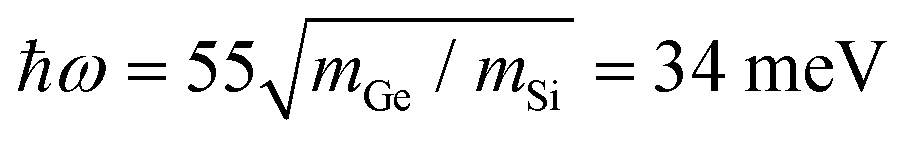 revealing that the frequency of the dominant peak in the PPhDOS of substitutional impurities, and hence the frequency of the vortex, is largely controlled by the impurity mass. Indeed, a vortex appears at this frequency, similar in morphology, but larger in size than the vortex of the Si–C3 defect. The vortex is shown in ESM Fig. S1 (ESI†), where we point out some additional features whose exploration would require much larger supercells than are currently practical.
Phonon vortices at point defects are present in other host materials. Monolayer h-BN is another honeycomb 2D material that consists of two different sublattices occupied by B and N atoms, respectively. It is worth noting that B and N atoms in h-BN possess different Born effective charges, leading to the presence of infrared-active phonon modes that generate electronic polarization through atomic displacements. The presence of phonon vortices at impurities in h-BN would be more interesting with respect to dielectric properties. When one N atom is replaced by a heavier P atom or a B atom is replaced by a heavier Al atom, formation of phonon vortices similar to those of Si–C3 are observed (Fig. 3), which suggests a common underlying mechanism for the generation of vortices in graphene and h-BN. The frequencies of these phonon vortices are within the acoustic-phonon regime of h-BN, i.e., the vortices are also resonant with pristine-h-BN phonon modes as is the case for Si defects in graphene.
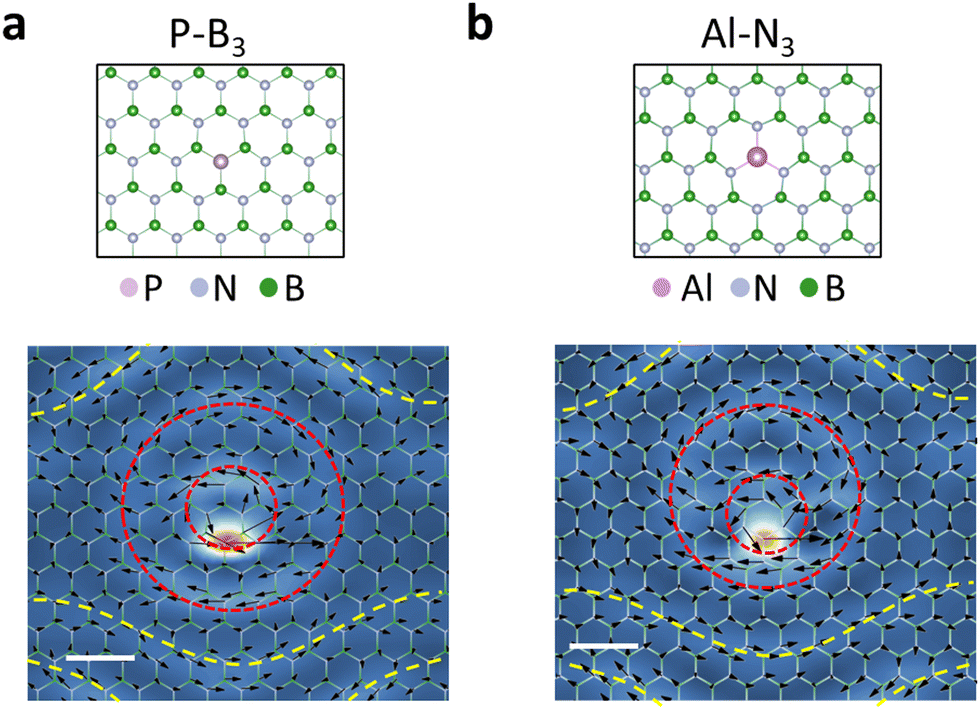 | ||
| Fig. 3 Phonon vortices in P–B3 and Al–N3 in h-BN. The P atom is buckled off the h-BN plane by 1.8 Å. The Al atom is off the h-BN plane by 1.3 Å. The P phonon vortex is observed at a frequency of 46 meV, only slightly lower than that of Al–N3 (48 meV) caused by the slightly heavier mass of P compared with Al. | ||
It is clear from the atomic-displacement maps of the vortices in Fig. 1 and 2 that the vortices are larger than the computational supercells, which raises questions about the effect of neighboring vortices on the vortex shape. Si–C3 vortices in adjacent 12 × 12 computational supercells are shown in Fig. 4a. That is the supercell used for the PPhDOS curves and the vortex map in Fig. 1b and d, respectively. Though computationally taxing, we performed calculations in which we quadrupled the supercell size for Si–C3 (the maps of the Si–C3 vortex in Fig. 1d and Fig. 2a are from 12 × 12 and 24 × 24 supercells, respectively, but are placed in a square periodic unit). The results shown in Fig. 4b reveal that the morphology and size of the vortex cores do not change noticeably. The dashed rhombi in Fig. 4b act as reference markers, guiding the readers’ eyes to recognize and compare the similarities in the vortex patterns observed within the respective supercells. In computational parlance, the vortex-core morphology is converged. The fact that the vortex appears in the graphene mode with energy at the primary peak in the PPhDOS on Si (Fig. 1b) corroborates this conclusion.
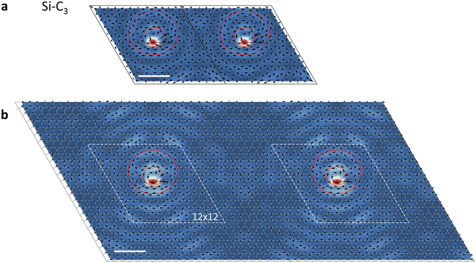 | ||
| Fig. 4 Phonon vortices in computational supercells of different sizes. (a) Atomic-displacement maps of Si–C3 phonon vortices in two adjacent 12 × 12 computational supercells. Red circles again illustrate the phonon vortices. The energy of the mode is 55 meV. (b) Atomic-displacement maps of Si–C3 phonon vortices in two adjacent 24 × 24 computational supercells. The frequency of the plotted mode is 57 meV, matching the energy of the peak in the PPhDOS obtained with 24 × 24 supercells. The two white dashed rhombi guide the eyes to identify the similarities with the two rhombi in panel a. Scale bars: 1 nm. | ||
On the other hand, Fig. 4b makes clear that the red circular patterns around the Si impurity continue outside the dashed romboids, i.e., the overall size of the vortex is much larger than what we see in the central panel of Fig. 1d. It is also clear that the distance between vortices is not large enough to allow the presence of pristine-graphene phonon waves, as we illustrated schematically in the side panels of Fig. 2a. Much larger supercells are needed for such features to materialize. Such calculations are not currently practical.
The vortices we described in this paper are unique to point defects, and are fundamentally different from chiral phonon waves.31,32 In a phonon vortex at a defect, all atoms execute small back-and-forth motions, in concert, in the directions indicated by the black arrows in our vortex maps, as in the case of conventional acoustic and optical phonons in crystals, but the arrows in a vortex are arranged in a roughly circular pattern around the defect. The atomic displacements of chiral phonons are not back and forth along an axis. Another difference is in the angular momentum of chiral phonons and vortices. All atoms participating in vortices vibrate back and forth along an axis, so that the net angular momentum about the central axis is zero (the contribution to the angular momentum of each atom is r × p half of the time and r × (−p) the other half of the time). In contrast, atoms in chiral phonons31,32 circle their equilibrium sites and have non-zero angular momentum, while the net angular momentum of the chiral mode depends on the relative phase of rotation of atoms in different sublattices.31,32
In summary, we performed extensive calculations of phonons at various point defects anchored by a heavy impurity in different 2D monolayer materials and found phonon vortices. The phonon vortices are characterized by back-and-forth displacements in concert in circular patterns. The formation of phonon vortices is attributed to the coupling between the vibrations of the heavy impurity atom and the propagating acoustic phonon waves of the host monolayer. We demonstrated that the behavior of phonon vortices depends on the local symmetry and mass of the defect and that phonon vortices at point defects exist in different host materials, namely graphene and h-BN. The question whether phonon vortices at point defects exist in 2D materials that consist of more than one plane of atoms and in three-dimensional materials remains an open question at this stage as accurate calculations are not practical. When vortices do exist, however, they are likely to impact thermal properties, especially thermal conductivity.
Methods
The DFT calculations were performed using the Vienna ab initio Simulation Package (VASP)33,34 with the projector-augmented-wave method.35 The Perdew–Burke–Ernzerhof36 version of the generalized gradient approximation (GGA)37 was used in all simulations. The plane-wave basis energy cut off is 600 eV. The calculational cells for Si- and N-doped graphene are 12 × 12 supercells, containing 288 atomic sites. Some calculations were done using 24 × 24 supercells containing 1152 atomic sites. Calculations for substitutional P at N sites and Al at B sites in h-BN were performed using 12 × 12 supercells. A vacuum region between graphene (or BN) sheets was set to 20 Å along the z direction to minimize periodic interactions. The k points were set as Γ-centered 3 × 3 × 1 for structural optimization and 1 × 1 × 1 for phonon calculations due to the expensive computational cost of the latter. For structural relaxation, the structures were relaxed until the atomic forces were less than 0.001 eV Å−1. The convergence tolerances for energy differences are 10−6 eV and 10−8 eV in relaxation and phonon calculations, respectively. Phonon calculations were performed using VASP combined with Phonopy using the density-functional-perturbation-theory (DFPT) method. For supercells, only Γ-point phonons were considered, while for pristine graphene, we also performed supercell calculations, so effectively 12 × 12 and 24 × 24 q-points were considered. The projected phonon densities of states are projected in the graphene (or BN) plane on corresponding atoms. A full width at half maximum (FWHM) of 8 meV was used to plot the projected phonon density of states. The arrows presenting atomic displacements are the in-plane components of corresponding phonon modes. The Si–C4 structure features four Si–C bonds with a slightly buckled configuration (the four C neighbors of Si rise by 0.2 Å above the graphene basal plane), whereas the Si–C3 features three Si–C bonds that are buckled (Si rises 1.8 Å above the graphene basal plane).Conflicts of interest
There are no conflicts to declare.Acknowledgements
Research at Vanderbilt University (D.-L. B., S. T. P.) was supported by the U.S. Department of Energy, Office of Science, Basic Energy Sciences, Materials Science and Engineering Division Grant No. DE-FG02-09ER46554 and by the McMinn Endowment. Calculations were performed at the National Energy Research Scientific Computing Center (NERSC), a U.S. Department of Energy Office of Science User Facility located at Lawrence Berkeley National Laboratory, operated under Contract No. DE-AC02-05CH11231. Research at UCAS was supported by the Beijing Outstanding Young Scientist Program with grant No. BJJWZYJH01201914430039 (W. Z.).References
- S. T. Pantelides, The electronic structure of impurities and other point defects in semiconductors, Rev. Mod. Phys., 1978, 50, 797–858 CrossRef CAS.
- C. Freysoldt, B. Grabowski, T. Hickel, J. Neugebauer, G. Kresse, A. Janotti and C. G. Van de Walle, First-principles calculations for point defects in solids, Rev. Mod. Phys., 2014, 86, 253–305 CrossRef.
- C. G. Van de Walle, P. J. Denteneer, Y. Bar-Yam and S. T. Pantelides, Theory of hydrogen diffusion and reactions in crystalline silicon, Phys. Rev. B: Condens. Matter Mater. Phys., 1989, 39, 10791–10808 CrossRef CAS PubMed.
- H. González-Herrero, J. M. Gómez-Rodríguez, P. Mallet, M. Moaied, J. J. Palacios, C. Salgado, M. M. Ugeda, J.-Y. Veuillen, F. Yndurain and I. Brihuega, Atomic-scale control of graphene magnetism by using hydrogen atoms, Science, 2016, 352, 437–441 CrossRef PubMed.
- G. Ye, Y. Gong, J. Lin, B. Li, Y. He, S. T. Pantelides, W. Zhou, R. Vajtai and P. M. Ajayan, Defects engineered monolayer MoS2 for improved hydrogen evolution reaction, Nano Lett., 2016, 16, 1097–1103 CrossRef CAS PubMed.
- S. T. Pantelides, Y. Puzyrev, X. Shen, T. Roy, S. DasGupta, B. R. Tuttle, D. M. Fleetwood and R. D. Schrimpf, Reliability of III–V devices-The defects that cause the trouble, Microelectron. Eng., 2012, 90, 3–8 CrossRef CAS.
- M. Buffolo, A. Caria, F. Piva, N. Roccato, C. Casu, C. De Santi, N. Trivellin, G. Meneghesso, E. Zanoni and M. Meneghini, Defects and reliability of GaN-based LEDs: Review and perspectives, Phys. Status Solidi A, 2022, 219, 2100727 CrossRef CAS.
- S. T. Pantelides, L. Tsetseris, M. J. Beck, S. N. Rashkeev, G. Hadjisavvas, I. G. Batyrev, B. R. Tuttle, A. G. Marinopoulos, X. J. Zhou, D. M. Fleetwood and R. D. Schrimpf, Performance, reliability, radiation effects, and aging issues in microelectronics – From atomic-scale physics to engineering-level modeling, Solid-State Electron., 2010, 54, 841–848 CrossRef CAS.
- X. Qian, J. Zhou and G. Chen, Phonon-engineered extreme thermal conductivity materials, Nat. Mater., 2021, 20, 1188–1202 CrossRef CAS PubMed.
- P. A. Fleury, J. F. Scott and J. M. Worlock, Soft Phonon Modes and the 110°K Phase Transition in SrTiO3, Phys. Rev. Lett., 1968, 21, 16–19 CrossRef CAS.
- D. J. Singh, Stability and phonons of KTaO3, Phys. Rev. B: Condens. Matter Mater. Phys., 1996, 53, 176 CrossRef CAS PubMed.
- R. Hillenbrand, T. Taubner and F. Keilmann, Phonon-enhanced light-matter interaction at the nanometre scale, Nature, 2002, 418, 159–162 CrossRef CAS PubMed.
- X. Zhao and D. Vanderbilt, Phonons and lattice dielectric properties of zirconia, Phys. Rev. B: Condens. Matter Mater. Phys., 2002, 65, 075105 CrossRef.
- M. Ma, F. Grey, L. Shen, M. Urbakh, S. Wu, J. Z. Liu, Y. Liu and Q. Zheng, Water transport inside carbon nanotubes mediated by phonon-induced oscillating friction, Nat. Nanotech., 2015, 10, 692–695 CrossRef CAS PubMed.
- J. Bardeen, L. N. Cooper and J. R. Schrieffer, Theory of superconductivity, Phys. Rev., 1957, 108, 1175 CrossRef CAS.
- J. Callaway, Model for lattice thermal conductivity at low temperatures, Phys. Rev., 1959, 113, 1046–1051 CrossRef CAS.
- L. Hornekaer, Stabilizing a C–H bond on graphene with sound, Science, 2019, 364, 331–332 CrossRef CAS PubMed.
- A. Steigerwald, J. Gregory, K. Varga, A. Hmelo, X. Liu, J. Furdyna, L. Feldman and N. Tolk, Study of depth-dependent radiation-induced defects using coherent acoustic phonon spectroscopy, MRS Online Proc. Libr., 2011, 1363, 1302–1303 Search PubMed.
- O. L. Krivanek, T. C. Lovejoy, N. Dellby, T. Aoki, R. W. Carpenter, P. Rez, E. Soignard, J. Zhu, P. E. Batson, M. J. Lagos, R. F. Egerton and P. A. Crozier, Vibrational spectroscopy in the electron microscope, Nature, 2014, 514, 209–212 CrossRef CAS PubMed.
- J. A. Hachtel, A. R. Lupini and J. C. Idrobo, Exploring the capabilities of monochromated electron energy loss spectroscopy in the infrared regime, Sci. Rep., 2018, 8, 5637 CrossRef PubMed.
- F. S. Hage, G. Radtke, D. M. Kepaptsoglou, M. Lazzeri and Q. M. Ramasse, Single-atom vibrational spectroscopy in the scanning transmission electron microscope, Science, 2020, 367, 1124–1127 CrossRef CAS PubMed.
- R. S. Qi, R. C. Shi, Y. H. Li, Y. W. Sun, M. Wu, N. Li, J. L. Du, K. H. Liu, C. L. Chen, J. Chen, F. Wang, D. P. Yu, E. G. Wang and P. Gao, Measuring phonon dispersion at an interface, Nature, 2021, 599, 399–403 CrossRef CAS PubMed.
- X. X. Yan, C. Y. Liu, C. A. Gadre, L. Gu, T. Aoki, T. C. Lovejoy, N. Dellby, O. L. Krivanek, D. G. Schlom, R. Q. Wu and X. Q. Pan, Single-defect phonons imaged by electron microscopy, Nature, 2021, 589, 65–69 CrossRef CAS PubMed.
- E. R. Hoglund, D. L. Bao, A. O'Hara, T. W. Pfeifer, M. S. B. Hoque, S. Makarem, J. M. Howe, S. T. Pantelides, P. E. Hopkins and J. A. Hachtel, Direct visualization of localized vibrations at complex grain boundaries, Adv. Mater., 2023, 35, 2208920 CrossRef CAS PubMed.
- M. Xu, D. L. Bao, A. Li, M. Gao, D. Meng, A. Li, S. Du, G. Su, S. J. Pennycook, S. T. Pantelides and W. Zhou, Single-atom vibrational spectroscopy with chemical-bonding sensitivity, Nat. Mater., 2023, 22, 612–618 CrossRef CAS PubMed.
- J. Bernholc, N. O. Lipari and S. T. Pantelides, Self-consistent method for point defects in semiconductors: application to the vacancy in silicon, Phys. Rev. Lett., 1978, 41, 895–899 CrossRef CAS.
- W. Zhou, M. D. Kapetanakis, M. P. Prange, S. T. Pantelides, S. J. Pennycook and J. C. Idrobo, Direct determination of the chemical bonding of individual impurities in graphene, Phys. Rev. Lett., 2012, 109, 206803 CrossRef PubMed.
- J. Serrano, J. Strempfer, M. Cardona, M. Schwoerer-Böhning, H. Requardt, M. Lorenzen, B. Stojetz, P. Pavone and W. J. Choyke, Determination of the phonon dispersion of zinc blende (3C) silicon carbide by inelastic x-ray scattering, Appl. Phys. Lett., 2002, 80, 4360–4362 CrossRef CAS.
- K. Venkatraman, B. D. A. Levin, K. March, P. Rez and P. A. Crozier, Vibrational spectroscopy at atomic resolution with electron impact scattering, Nat. Phys., 2019, 15, 1237–1241 Search PubMed.
- A. S. Barker and A. J. Sievers, Optical studies of the vibrational properties of disordered solids, Rev. Mod. Phys., 1975, 47, S1–S179 CrossRef.
- H. Zhu, J. Yi, M.-Y. Li, J. Xiao, L. Zhang, C.-W. Yang, R. A. Kaindl, L.-J. Li, Y. Wang and X. Zhang, Observation of chiral phonons, Science, 2018, 359, 579–582 CrossRef CAS PubMed.
- L. Zhang and Q. Niu, Chiral phonons at high-symmetry points in monolayer hexagonal lattices, Phys. Rev. Lett., 2015, 115, 115502 CrossRef PubMed.
- G. Kresse and J. Furthmüller, Efficiency of ab-initio total energy calculations for metals and semiconductors using a plane-wave basis set, Comput. Mater. Sci., 1996, 6, 15–50 CrossRef CAS.
- G. Kresse and J. Furthmüller, Efficient iterative schemes for ab initio total-energy calculations using a plane-wave basis set, Phys. Rev. B: Condens. Matter Mater. Phys., 1996, 54, 11169–11186 CrossRef CAS PubMed.
- P. E. Blöchl, Projector augmented-wave method, Phys. Rev. B: Condens. Matter Mater. Phys., 1994, 50, 17953–17979 CrossRef PubMed.
- J. P. Perdew, K. Burke and M. Ernzerhof, Generalized gradient approximation made simple, Phys. Rev. Lett., 1996, 77, 3865–3868 CrossRef CAS PubMed.
- J. P. Perdew, J. A. Chevary, S. H. Vosko, K. A. Jackson, M. R. Pederson, D. J. Singh and C. Fiolhais, Atoms, molecules, solids, and surfaces: Applications of the generalized gradient approximation for exchange and correlation, Phys. Rev. B: Condens. Matter Mater. Phys., 1992, 46, 6671–6687 CrossRef CAS PubMed.
Footnote |
| † Electronic supplementary information (ESI) available. See DOI: https://doi.org/10.1039/d3nh00433c |
| This journal is © The Royal Society of Chemistry 2024 |