
 Open Access Article
 This Open Access Article is licensed under a Creative Commons Attribution-Non Commercial 3.0 Unported Licence
Boosting photocurrent of anodized Nb2O5 by synergetic post-synthesis electrochemical treatment†
Wallas T.
Menezes
,
Roger
Gonçalves
 and
Ernesto C.
Pereira
*
and
Ernesto C.
Pereira
*
Chemistry Department, Federal University of São Carlos, Mailbox 676, CEP 13565-905, São Carlos – SP, Brazil. E-mail: ernesto@ufscar.br
First published on 29th May 2024
Abstract
Hydrogen has emerged as a promising alternative to fossil fuels due to its environmental benefits. Niobium pentoxide (Nb2O5) is an effective photocatalyst for water splitting, but its narrow bandgap limits efficiency. However, cathodic polarization doping can be used to shift the bandgap of Nb2O5 to the visible light range, plus tuning its band relative positions, making it a more efficient photocatalyst. This method is simple, inexpensive, and provides precise control over the amount of dopants in the Nb2O5 matrix. This will allow green hydrogen production from a broader range of light sources. To this end, niobium pentoxide was produced by anodizing metallic niobium with subsequent thermal and cathodic treatment of the obtained samples. The resulting electrodes were characterized by their morphology and electrochemical and photoelectrochemical properties. Cathodically treated films were observed to present a much higher photocurrent (about 2.1 times) than those not submitted for any treatment. Besides, it is even more significant than thermally treated ones. Furthermore, the cathodic treatment samples are exceptionally stable, remaining observed for more than 30 days. Therefore, it is concluded that Nb2O5 films can significantly improve their properties by applying simple and quick treatments, making them an even more promising material for application in water electrolysis.
1. Introduction
The efficient utilization of solar energy is a paramount goal of modern science and engineering, given its clean, abundant, and inexhaustible nature. From a different perspective, considering environmental pollution and human health, hydrogen energy stands out as one of the most sustainable energy sources. It boasts the highest heating capacity, approximately 150 kJ mol−1, which is 2.4 and 4 times greater than methane and coal, respectively.1,2 Hence, hydrogen has been proposed as a promising alternative energy resource to replace fossil fuels, especially if it is produced using photoelectrochemical methods.Electrochemical green hydrogen can be produced by splitting water molecules into hydrogen and oxygen using electricity from renewable sources such as solar and wind power. Solar light can also assist this electrochemical reaction, i.e., using a photoelectrochemical process. In this case, a semiconductor has charge carriers generated by sunlight, leading to the break of water molecules photoelectrochemically to generate green H2. Many different materials have been proposed for this reaction,1 among them, niobium pentoxide (Nb2O5) has stood out for its high efficiency, low cost, and photostability, as well as the bands' positions suitable for the water molecule's redox.2 In addition, it can produce hydrogen from various feedstocks, including methanol, ethanol, natural gas, and biomass.3–5
Anodizing can be used to synthesize niobium pentoxide, resulting in the formation of a dense and adherent oxide layer. This oxide layer enhances corrosion resistance and exhibits excellent biocompatibility, making it promising for biomedical applications like implants and surgical instruments.6 Besides, anodization is particularly attractive due to its tunability; parameters such as voltage, electrolyte composition, and process duration can be adjusted to precisely control the thickness and properties of the oxide layer.7 Many different morphologies and structures that can be obtained as nanotubes,8 porous9 or nanoporous.10 Then, the film application and/or purpose will dictate the desired morphology, which can be obtained by controlling the above-described variables.
However, the technological use of Nb2O5 is limited due to its bandgap value (3.4 eV), which requires UV irradiation with a wavelength shorter than 365 nm to activate the photocatalysis effectively.11 As UV light is a small fraction (5%) of solar radiation compared to visible light (45%), any bathochromic shift in light absorption will have a significant impact on the usefulness of this material in photoconversion. For this reason, different techniques have been proposed to increase photoconversion efficiency. Among them is obtaining specific nanostructures, such as nanotubes, and doping these materials.12,13
From a different point of view, the doping process allows changing the material's band structure without significantly affecting the composition and crystalline structure. This method is used to promote changes in the properties of the photocatalyst. It consists of replacing atoms of the crystal lattice of the host material with one or more elements to generate specific electronic, structural, and/or optical properties.14–16 These processes can also change the wavelength of light absorption and the relative position of bands to increase catalytic activity.
The cathodic doping procedure is one way to dope a semiconductor without inserting other elements into its matrix,17 a process in which the semiconductor is made negatively charged by applying a negative external electrochemical potential. This leads to the formation of stabilized Nb4+ centers and the incorporation of positive cations from the solution. It is a valuable technique for doping semiconductors because it is simple, inexpensive, and versatile. It also allows a controllable process, making it ideal for precisely doping semiconductors. This can be done by immersing the semiconductor in an electrolyte solution and applying a more negative voltage than the open circuit potential.
Cathodic-doped niobium pentoxide films are rarely reported in the literature. However, these few papers report significant effects on the material's properties. Khan et al.17 reported the development of a simple and effective method for self-doping niobium pentoxide by cathodic polarization. The technique involves electrochemically reducing Nb2O5 in a phosphate buffer solution at −2.5 V vs. Ag/AgCl/KClsat. This results in the reduction of Nb5+ to Nb4+, which increases the material's charge carrier density and conductivity. The authors tested the self-doped electrode for photoelectrocatalytic degradation of reactive red 120 (RR120) dye. They found it had a significantly higher photocurrent and photocatalytic activity than the undoped Nb2O5. This result suggests that self-doping by cathodic polarization is a promising method for improving the photoelectrocatalytic performance of Nb2O5-based photoanodes.
On the other hand, Zhang et al.18 investigated the effects of niobium pentoxide and gadolinium oxide (Gd2O3) doping on the boron volatility and activity between glass seals and lanthanum-containing cathodes. The authors found that both Nb2O5 and Gd2O3 doping increase the glass seals' network connectivity, reducing the boron volatility and activity. This is important because boron contamination of the cathode can lead to performance degradation. The authors also found that niobium oxide doping is more effective than gadolinium oxide doping in reducing boron volatility and activity. Realize then that the insertion of different elements in the host crystal lattice allows modulation of the semiconductor band gap, as it inserts new bands within the forbidden region; these new bands are inserted close to the conduction bands (BC) or the valence band (BV). In this way, there is a reduction in the energy required for electronic excitation, which leads to a bathochromic shift in the absorption spectrum of the resulting material.19,20
Finally, it is essential to mention that although it is not Nb2O5, the work of Zhou et al.21 describes the co-doping of Nb3O8− both with N atoms and with reduced Nb, that is, cathodic doping. In this work, the authors tested both electrodes manufactured with N doping, reduced-Nb doping, and N/reduced-Nb codoping for comparative studies on the doping effect for photocatalytic hydrogen evolution. Thus, the authors found that nitrogen doping introduces an impurity energy level just above the valence band (VB) of Nb3O8−, while reduced niobium doping introduces an intermediate energy level just below the conducting band. Simultaneous N/rNb codoping introduces these intermediate energy levels and an exotic Nbn+ (where n ≤ 4) level, further narrowing the band gap. These changes in the material's electronic structure lead to enhanced photo-absorption in the UV-visible region and improved charge separation during photocatalysis. This makes N/rNb codoped a promising photocatalyst for hydrogen production.
Given the discussion above, the present work proposes synthesizing materials with photoactivity and efficiently converting solar energy to photoelectrochemical water splitting. The photocatalysts are formed by Nb2O5 obtained by anodizing metallic niobium with subsequent treatment to increase crystallinity and, after, its photoactivity by electrochemical self-doping. Thus, this research, focusing on enhancing Nb2O5 properties through cathodic doping, contributes to this global effort by offering a simple, inexpensive, and effective method for hydrogen production from a broader range of light sources.
2. Experimental section
2.1. Electrodes preparation
The electrode preparation followed some steps, which will be described next. Each of them produced a sample to be characterized. Thus, three distinct samples were compared: one only anodized (without any additional treatment), one after heat treatment, and one after both heat and anodic treatment. The steps of the electrode preparation can be seen in summary in the diagram in Fig. 1.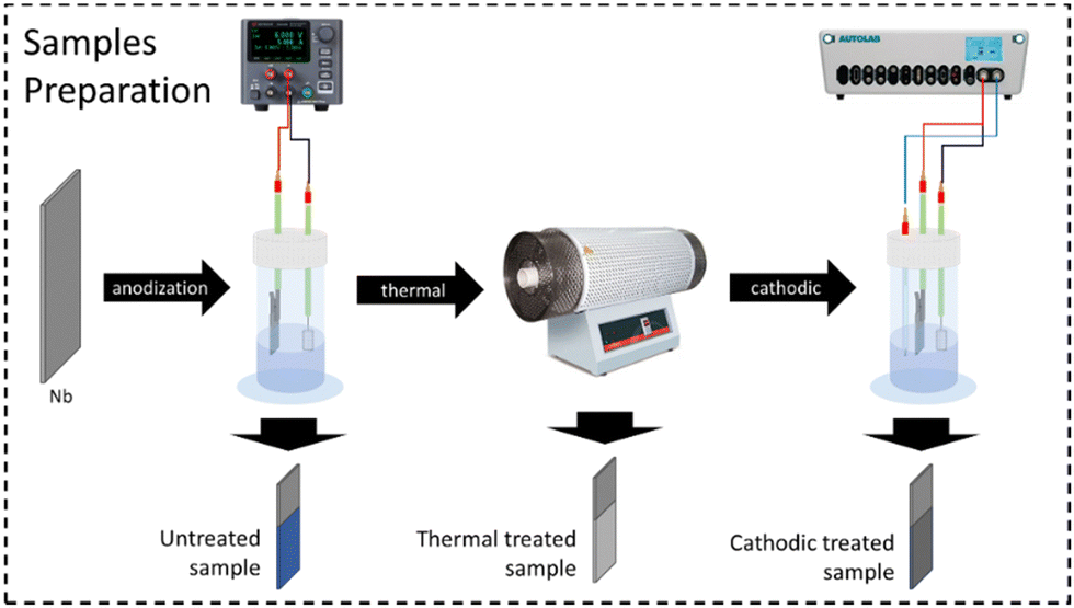 | ||
| Fig. 1 Scheme of the procedure used to obtain the different samples. | ||
![[thin space (1/6-em)]](https://www.rsc.org/images/entities/char_2009.gif) :HNO3:H2O, in a 1:4:5 volumetric ratio. The electrodes were kept for 10 min, washed with abundant water ultrapure, and dried with N2 flow.
:HNO3:H2O, in a 1:4:5 volumetric ratio. The electrodes were kept for 10 min, washed with abundant water ultrapure, and dried with N2 flow.
2.2. Characterization
The Raman spectra were obtained using a micro-Raman Horiba iHR550 to understand the samples' vibrational states. The crystallinity of the oxides obtained was evaluated by powder X-ray diffraction collected using a Shimadz diffractometer (XRD6100, CuKα radiation) in the 2θ range from 20° to 80° with a step of 0.02° and at a scanning speed of 2° min−1. The films' morphology was studied by atomic force microscopy (AFM) and scanning electron microscopy (SEM). The AFM images were obtained at intermittent mode using a nano-observer AFM microscope. Meanwhile, the SEM images were obtained in backscatter mode using a Philips XL-30 FEG. The film thickness was obtained by cross-sectional imaging, also using the SEM technique. As morphological parameters were calculated, all images and their respective measurements were taken in triplicates in different regions of the films for a more representative sampling.Under light measurements, use a Thorlabs lamp 365 nm with a power of 10 mW cm−2. All electrochemical measurements were performed on an Autolab Potentiostat/Galvanostat model 302N equipped with a FRA32 module. For these characterizations, a conventional single-compartment, three-electrode cell was used, where Nb2O5 films were used as the working electrode (WE), as the counter electrode (CE) in a platinum network, and Ag/AgCl/KClsat as the reference electrode (RE). On/off linear voltammetry was performed from −0.15 V up to 2.0 V at 50 mV s−1 with an on/off illumination of 8.33 mHz switch. On/off chronoamperometry was performed at 1.2 V for 800 s. This method allows for the evaluation of photocurrent as a function of the scanning potential, allowing one to choose the best working potential assertively. The electrochemical impedance spectroscopy was performed from 10 kHz to 10 mHz at a DC potential of 1.2 V and AC perturbation of 10 mVrms. The potential chosen for the chronoamperometric and spectroscopic impedance characterizations was due to a choice between obtaining a higher photocurrent value and solvent stability limit and avoiding photodegradation of the active material.
Finally, the electronic structure of the materials was estimated using bandgap information obtained by Tauc Plot from diffuse reflectance data taken on a UV-vis Cary 7000 spectrophotometer and flat-band potential information obtained from Mott–Schottky plots obtained at 1.0 kHz. The impedance data was performed at 1.2 V from 10 kHz to 10 mHz with a perturbation potential of 10 mV. The EIS measurement was performed in both cases, with and without illumination, so it would be possible to estimate the properties of excitons created due to light excitation later.
3. Results and discussion
Fig. 2a shows the Raman spectra of the samples, which exhibit the typical Raman shifts for the Nb2O5 orthorhombic phase chemical groups.22 The broad band around 700 cm−1 is signed to the symmetric stretching of the polyhedral Nb–O. Additional bands below 300 cm−1 could be attributed to stretching the Nb–O–Nb bonds. On the other hand, the X-ray diffraction patterns of Nb2O5 samples are shown in Fig. 2b. However, all samples show the peaks characteristic of the orthorhombic phase (phase T), according to joint committee on powder diffraction standards (JCPDS) card no. 27-1003.23 It is possible to notice that the intensity of the peaks is higher after the heat treatment, indicating a significant increase in the material's crystallinity, as expected. It is interesting to note that the anodized film, even without heat treatment, already exhibits high crystallinity; this fact occurs because the film was grown in such a way that electrolytic breakdown occurred, therefore generating sparks on the surface of the growing film due to the enormous increase in local temperature, thus inducing an increase in crystallinity.24–26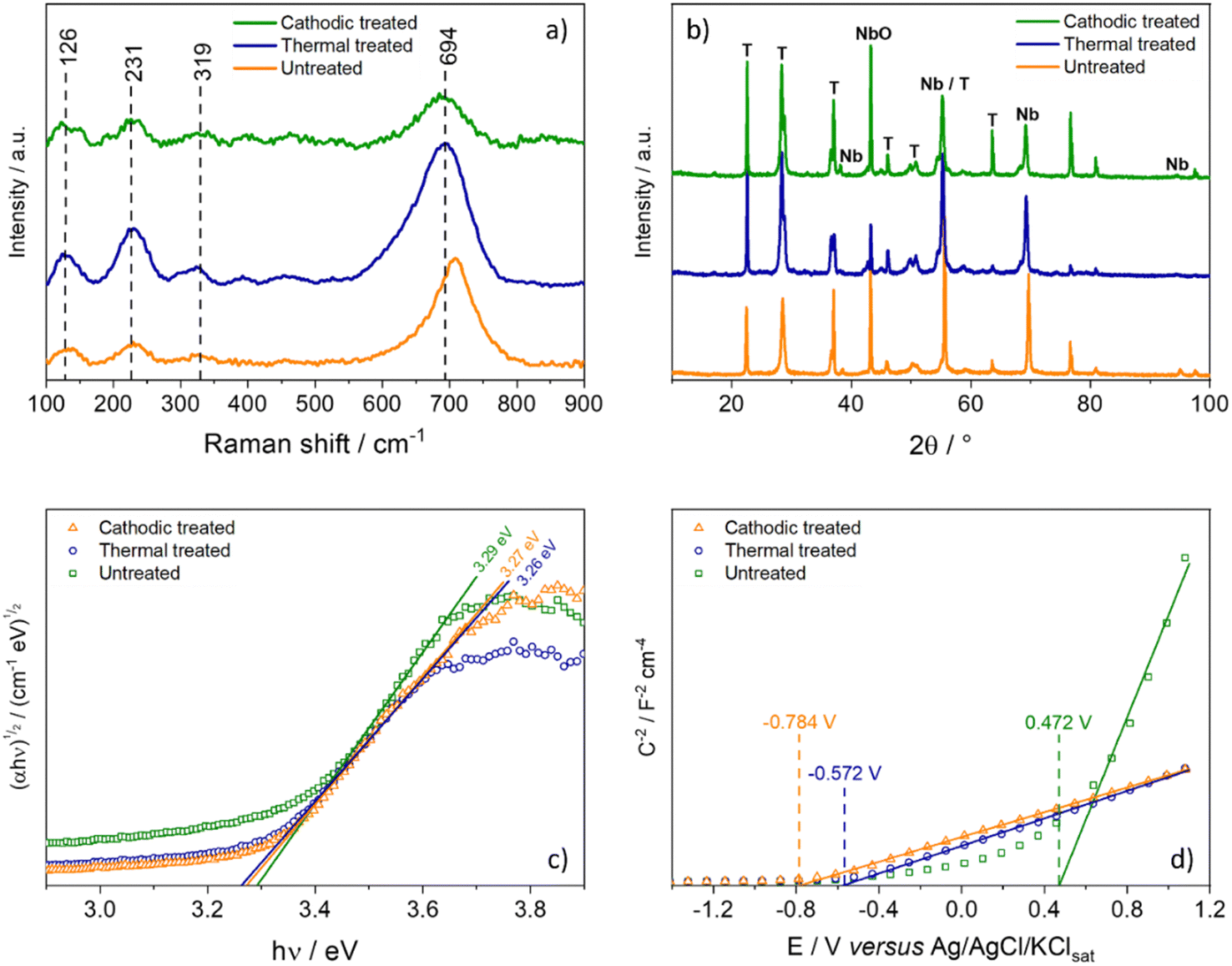 | ||
| Fig. 2 (a) Raman spectra, (b) DRX spectra, (c) Tauc plot, and (d) Mott–Schottky plot for the sample with different treatment levels. | ||
Fig. 2c shows the Tauc plot for indirect bandgap that does not present significant changes in the bandgap value due to the treatment applied, which is consistent with the literature although slightly lower, 3.4 eV.2 Thus, any change in the photocurrent values could be attributed to other changes in the material's electronic structure. This fact is evidenced by analyzing the Mott–Schottky graph (Fig. 1d), where it is possible to estimate the flat band potential of each electrode. The effect of heat treatment causes a very sharp shift in the Efb to more negative potentials. The cathodic treatment intensifies this effect for 0.132 V more negative.
Using the bandgap energy and flat-band potential information, it is possible to outline the band diagram, which will guide discussions involving each sample's performance (Fig. 3). Since the bandgap values of the samples are very close, the only observable change in the band diagram is their position in relation to the scale, in this case, versus NHE. Thus, considering this, all films obtained can be used for water splitting according to their respective band positions.
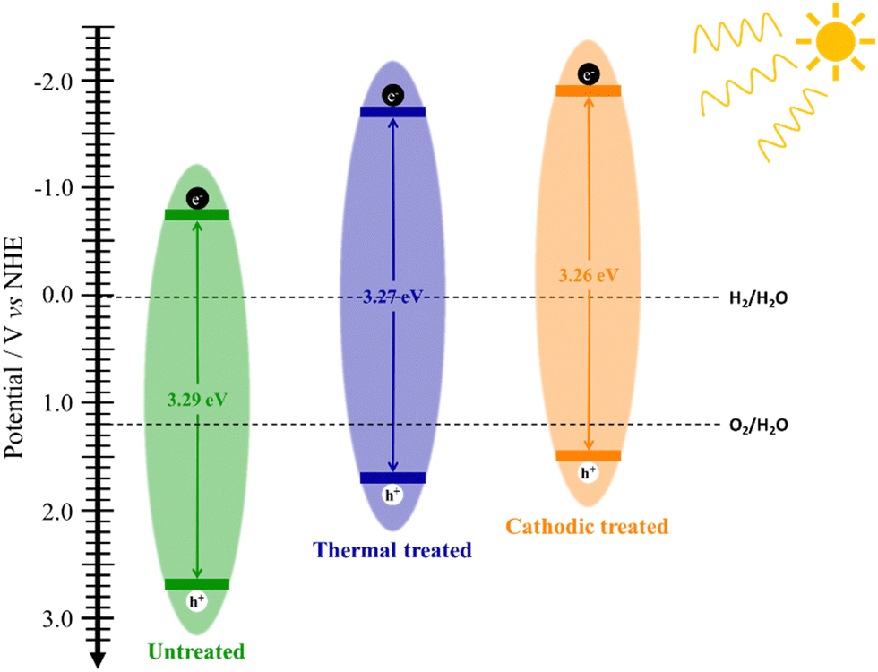 | ||
| Fig. 3 Band diagram of anodic films obtained by different treatment methods. | ||
The SEM images (Fig. 4) reveal that all the films presented a morphology very close to a coral reef. However, it is observable that the thermal treatment leads to an increase in the agglomerate size of the film. Consequently, subsequent anodic treatment leads to pore formation again, increasing the film area. This fact is corroborated by the topological information obtained by the AFM, allowing the calculation of the average roughness of each film, which gives a clearer idea of any morphological changes suffered by the film due to any treatment stage. There is a slight decrease of 8.57% in the values (from 154.9 to 141.6 nm) of the untreated film for the thermally treated one and then a significant increase (from 141.6 to 220.6 nm) of 56.8% after the cathodic treatment. The 3D topographic images of the samples can be seen in S1 (ESI†). Furthermore, cross-sectional SEM images allow for obtaining the thickness of the anodic films. Table 1 summarizes the parameters and associated errors obtained by AFM and transversal SEM image analysis.
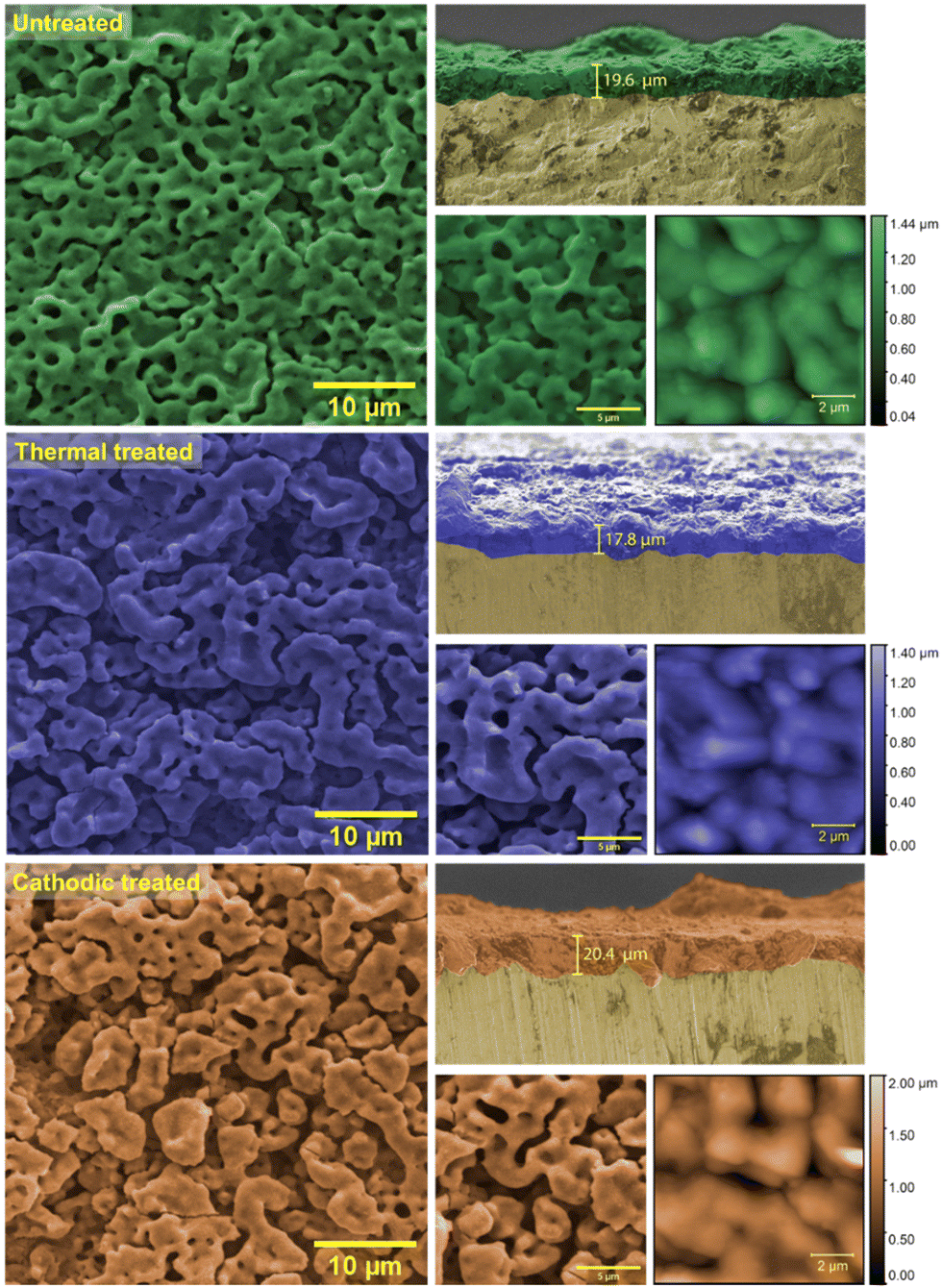 | ||
| Fig. 4 SEM micrographs at 5k and 10k× magnification of the electrode's surface and cross-section and AFM images of 10 × 10 μm. | ||
| Untreated | Thermal treated | Cathodic treated | |
|---|---|---|---|
| Mean thickness (μm) | 19.6 ± 0.37 | 17.8 ± 1.8 | 20.4 ± 2.2 |
| Mean roughness (Sa, nm) | 154.9 ± 30.5 | 141.6 ± 31.3 | 220.6 ± 42.6 |
| Mean square roughness (Sq, nm) | 187.3 ± 32.0 | 168.0 ± 35.1 | 267.5 ± 62.5 |
As expected, the heat treatment causes a slight decrease in the thickness due to the film sintering process (around 12.8%). On the other hand, there is a thickening of the anodic film due to the polarization treatment in an oxidizing medium, which favors the growth of more oxide film. Although not expected in the case of a cathodic process. Therefore, it is suggested that the conversion of the Nb5+ species into Nb4+ creates optical defects in electrons. This means that cations from the solution can be absorbed to achieve local charge neutralization. Also, the possibility of electronic defects leading to structural reorganization is raised, reflected in the film macroscopically as an increase in thickness. Finally, considering the relative errors, the values are not expressive and perhaps should not be discussed at length, although the roughness values present substantial changes.
The electrochemical impedance spectroscopy technique is powerful and versatile for characterizing photoactive materials. One way to use this technique is to run it without light and under illumination so that the differences between the two spectra are just a consequence of the magnitude of the photocurrent. Thus, Fig. 5a–c show the impedance spectra in the dark, which makes it possible to see that the impedance follows the distribution of flat band potential values. Therefore, it is possible to infer that the heat treatment's electronic modification directly affects the oxide film's charge transfer resistance. The Bode phase is normalized to solution resistance equal to zero (Rsol = 0) to observe the information correctly. The time constants also follow the same pattern, seen in the Bode phase, suggesting that post-synthesis heat treatment improves the film's electrochemical properties in terms of the charge-transfer rate. In contrast, cathodic treatment presents a substantial improvement in the mobility and lifetime of the excitons, which explains the significant increase in the photocurrent of this sample compared to the others.
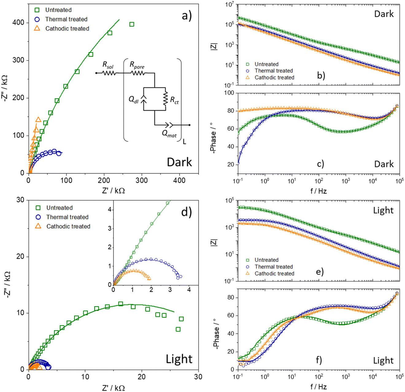 | ||
| Fig. 5 (a) Nyquist, (b) Bode |Z| and (c) Bode Phase plots for samples in the dark, and (d) Nyquist, (e) Bode |Z| and (f) Bode phase plots for samples with illumination. The Bode phase is normalized to Rsol = 0. | ||
However, the most remarkable result is observable in the data obtained under illumination, present in Fig. 4d–f. Initially, it was possible to notice an order-of-magnitude reduction in the impedance values, in addition to the fact that the semicircles are now well-defined and visible. Consequently, the time constants shifted to higher frequencies, that is, lower times.
Nevertheless, it is necessary to adjust using some data processing model to obtain more information from the impedance spectra. Thus, as a porous material, the transmission line model was adopted, presented as an inset image in Fig. 5a.27,28 The model consists of a first resistance, attributed to the solution resistance (Rsol), in series with another resistance, the pore resistance (Rpore), which occurs due to the difference in availability of the electrolyte within the solution and the pores. Then, in the branch that describes the material/electrolyte interface, the charge transfer resistance (Rct) and the pseudocapacitance to the electrical double layer are in parallel, represented by a constant phase element (Qdl). Finally, because it is a highly porous oxide, in the branch that describes the material, a constant phase element (Qmat) is necessary to explain the delays in the movement of charge carriers. The parameters obtained by adjusting the spectra are summarized in Table 2, along with other parameters obtained by Mott–Schottky: number of charge carriers (ND) and flat-band potential (Efb). The equivalent capacitance was calculated using the formula described by Chang.29 The other calculated values were charge transfer constant (kct), charge carrier mobility (μ), and lifetime (τ) using impedance data.30–32
| Untreated | Thermal treated | Cathodic treated | ||||
|---|---|---|---|---|---|---|
| Dark | Light | Dark | Light | Dark | Light | |
| R pore/Ω cm−2 | 911.720 | 723.650 | 46.797 | 4.380 | 3.146 | 0.718 |
| R ct/kΩ cm−2 | 179.640 | 36.324 | 13.765 | 0.379 | 1.471 | 1.332 |
| C dl/μF cm−2 | 0.292 | 0.624 | 0.929 | 1.195 | 3.770 | 5.484 |
| C mat/μF cm−2 | 1.135 | 1.884 | 0.776 | 1.200 | 0.445 | 2.489 |
| χ 2 | 2.31 × 10⁻⁵ | 2.24 × 10⁻⁵ | 5.73 × 10⁻⁵ | 3.14 × 10⁻⁵ | 3.62 × 10⁻⁵ | 4.48 × 10⁻⁵ |
| N D/×1018 cm−3 | 0.6000 | 29.78 | 97.62 | |||
| E fb/V vs. Ag/AgCl/KClsat | 0.472 | −0.572 | −0.784 | |||
| k ct/s−1 | 0.162 | 6.748 | 25.632 | |||
| μ/mm2 V−1 s−1 | 3.623 | 62.97 | 85.65 | |||
| τ/ms | 0.0141 | 0.245 | 0.333 | |||
Fig. 6a shows the linear voltammetric curves obtained in the light on/off regime. It is observed that at low potentials, below 0.2 V, although there is a high photoactivity, the recombination rate is also appreciable, and this decreases as the potential increases.33 However, it is necessary to consider both photodegradation and electrodegradation by using too high potentials under lighting. Thus, 1.2 V was chosen as the working potential, which presented a good balance between the amount of photocurrent and the material's durability. Although the recombination rate is lower for the post-treated materials, the cathode-treated material is slightly lower.
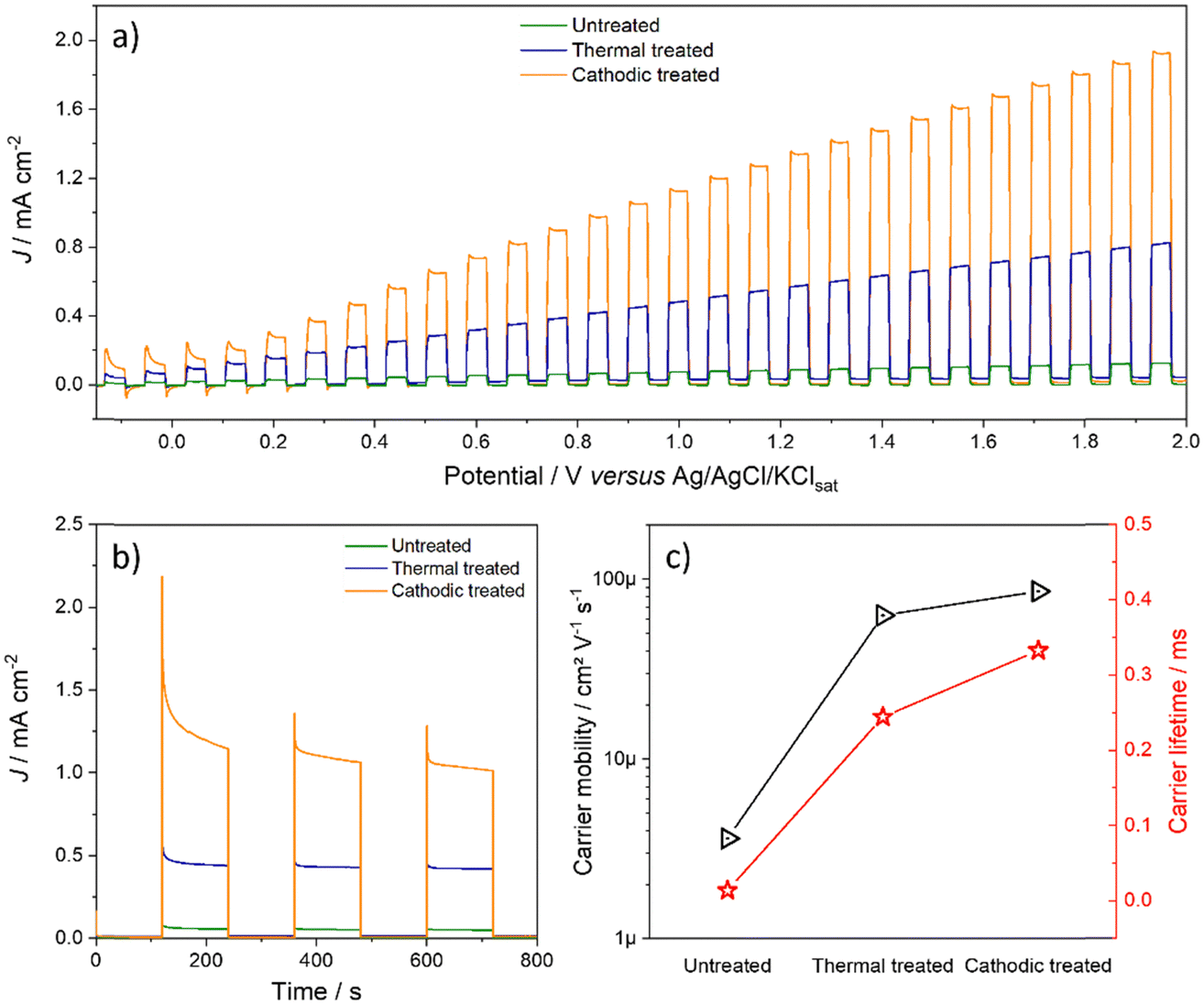 | ||
| Fig. 6 (a) On/off linear voltammetry, (b) on/off chronoamperometry at 1.2 V, and (c) charge carrier mobility and lifetime of freshly synthesized electrodes. | ||
To corroborate these statements, using data from electrochemical impedance spectroscopy in the light, it was possible to estimate the parameters of the excitons according to the relationships described by Garcia-Belmont and collaborators.31,34 The longer the charge carrier lifetime, the better it is, as it does not undergo recombination as soon as it is generated and can be used usefully. Likewise, greater mobility of the carrier allows it to travel inside the material so that it can be collected by the load collector and/or transferred to the species in solution. It is evident that the thermal treatment enormously increases the quality of the electron–hole pair since its lifetime and mobility increase orders of magnitude. On the other hand, although anodic doping increases these parameters even more, this does not occur markedly. However, the synergistic effect of all the modifications that samples underwent after both treatments led to a significant increase in photocurrent, as explained later.
Once the samples produced after the cathodic treatment exhibited a high photocurrent, it was questioned whether the treatment was durable or reverted after some time since it was a matter of inserting negative defects in the oxide crystalline network. Thus, photocurrent measurements were performed to compare the results after synthesis, after 0.67 day (i.e.,16 h), and after 5 and 30 days (Fig. 7). Surprisingly, the photocurrent did not decay with time; after a few hours in which the material was synthesized and thermally treated and then cathodically, there was a 2× increase in the photocurrent value, suggesting that during the period after cathodic polarization, the crystal lattice of the oxide tries to undergo some relaxation after the insertion of Nb4+ species, to improve the performance of the charge carriers. After 5 days, an increase in property was still observed, although much less pronounced. It is possible to attribute this increase after the anodic doping process to the defects introduced in the film requiring some stabilization, which occurs slowly over time. Considering this slow stabilization, the diffusion of defects can then be associated with more thermodynamically stable positions, improving the photocurrent. However, after 30 days under storage, the material lost photovoltaic properties; however, it remained superior (1.6×) to the newly synthesized material.
 | ||
| Fig. 7 (a) On/off linear voltammetry and (b) chronoamperometry at 1.0 V of aged films at different periods (freshly prepared and after 0.67 (16 h), 5 and 30 days). | ||
Therefore, it is clear that the homodefects added by cathodic treatment are permanent and give the material survival in the face of aging. However, further studies on accelerated electrochemical aging should be conducted to analyze their reactivity and impact on photomaterial properties.
4. Conclusions
It is possible to conclude that anodization is an efficient way of producing in situ a material capable of high photocatalytic activity, in addition to being characterized as a viable post-treatment for the controlled addition of defects in the material. Thermal treatment is necessary to produce a material resistant to leaching and considerably improve its photovoltaic properties. However, it was with the addition of Nb4+ species that it was possible to obtain an impressive photocurrent. The increase in photocatalytic properties was evaluated initially using voltammetry; however, it was possible to understand the extent of the improvement with a deeper study of electrochemical impedance spectroscopy. The excitons considerably improved mobility and lifetime, reducing the recombination rate and busting the charge transfer rate, an essential aspect of water splitting. It is impressive to note that doping done simply by reducing the portion of Nb5+ ions has such a significant and lasting effect on the photoelectrochemical properties of the material, making this material, already widely targeted for water splitting, further increase its applicability.Conflicts of interest
There are no conflicts to declare.Acknowledgements
The authors acknowledge the financial support provided by the Brazilian funding agencies, which include the Brazilian National Council for Scientific and Technological Development - CNPq (grant no. 465571/2014-0, 407878/2022-0), São Paulo Research Foundation (grant no. 2013/07296-2, 2017/11986-5, 2021/12394-0), Coordenação de Aperfeiçoamento de Pessoal de Nível Superior (CAPES – Finance Code 001). The authors also thank Shell for the strategic importance of the support given by the ANP (National Agency for Petroleum, Natural Gas and Biofuels) through the regulation of the R&D fee.References
- Z. Liu, Y. Yu and X. Zhu, et al., Semiconductor heterojunctions for photocatalytic hydrogen production and Cr(VI) Reduction: A review, Mater. Res. Bull., 2022, 147, 111636, DOI:10.1016/j.materresbull.2021.111636.
- Y. Zhang, H. Zhao and X. Zhao, et al., Narrow-bandgap Nb2O5 nanowires with enclosed pores as high-performance photocatalyst, Sci. China Mater., 2019, 62(2), 203–210, DOI:10.1007/s40843-018-9308-7.
- M. Joya, J. Barba Ortega and A. Raba Paez, et al., Synthesis and Characterization of Nano-Particles of Niobium Pentoxide with Orthorhombic Symmetry, Metals, 2017, 7, 142, DOI:10.3390/met7040142.
- H. Mohan, S. Vadivel and M. Fujii, et al., PdS Coupled Nb2O5 Superstructure for Photocatalytic Overall Water Splitting, ChemCatChem, 2023, 15(3) DOI:10.1002/cctc.202201212.
- M. I. Taipabu, K. Viswanathan and W. Wu, et al., A critical review of the hydrogen production from biomass-based feedstocks: Challenge, solution, and future prospect, Process Saf. Environ. Prot., 2022, 164, 384–407, DOI:10.1016/j.psep.2022.06.006.
- H. M. Wadullah, M. Talib Mohammed and T. Khalid Abdulrazzaq, Structure and characteristics of Nb2O5 nanocoating thin film for biomedical applications, Mater. Today Proc., 2022, 62, 3076–3080, DOI:10.1016/j.matpr.2022.03.229.
- A. C. V. Bianchin, G. R. Maldaner and L. T. Fuhr, et al., A Model for the Formation of Niobium Structures by anodization, Mater. Res., 2017, 20, 1010–1023, DOI:10.1590/1980-5373-mr-2016-0392.
- C. Moseke, C. Lehmann and T. Schmitz, et al., Nanostructuring of Refractory Metal Surfaces by Electrochemical Oxidation: Nb and the Binary Systems Ti-Ta and Nb-Ta, Curr. Nanosci., 2013, 9, 132–138, DOI:10.2174/1573413711309010022.
- J. Choi, J. H. Lim and S. C. Lee, et al., Porous niobium oxide films prepared by anodization in HF/H3PO4, Electrochim. Acta, 2006, 51, 5502–5507, DOI:10.1016/j.electacta.2006.02.024.
- N. Alias, Z. Hussain and W. K. Tan, et al., Nanoporous anodic Nb2O5 with pore-in-pore structure formation and its application for the photoreduction of Cr(VI), Chemosphere, 2021, 283, 131231, DOI:10.1016/j.chemosphere.2021.131231.
- G. Ramírez, S. E. Rodil and S. Muhl, et al., Amorphous niobium oxide thin films, J. Non Cryst. Solids, 2010, 356, DOI:10.1016/j.jnoncrysol.2010.09.073.
- C. D. Gómez and J. E. Rodríguez-Páez, The effect of the synthesis conditions on structure and photocatalytic activity of Nb2O5 nanostructures, Proc. Appl. Ceram., 2018, 12(3), 218–229, DOI:10.2298/PAC1803218G.
- C. Cui, R. Guo and E. Ren, et al., Facile hydrothermal synthesis of rod-like Nb2O5/Nb2CTx composites for visible-light driven photocatalytic degradation of organic pollutants, Environ. Res., 2021, 193, DOI:10.1016/j.envres.2020.110587.
- P. Wen, L. Ai and F. Wei, In-situ synthesis of crystalline Ag-Nb2O5 nanobelt clusters with enhanced solar photo-electrochemical performance for splitting water, Mater. Des., 2017, 131(5), 219–225, DOI:10.1016/j.matdes.2017.06.034.
- F. Trivinho-Strixino, F. E. G. Guimarães and E. C. Pereira, Luminescence in Anodic ZrO2 Doped with Eu(III)ions, Mol. Cryst. Liq. Cryst., 2008, 485, 766–775, DOI:10.1080/15421400801913444.
- W. Cho, Y. J. Lim and S.-M. Lee, et al., Facile Mn Surface Doping of Ni-Rich Layered Cathode Materials for Lithium Ion Batteries, ACS Appl. Mater. Interfaces, 2018, 10, 38915–38921, DOI:10.1021/acsami.8b13766.
- S. U. Khan, S. Hussain and J. A. L. Perini, et al., Self-doping of Nb2O5NC by cathodic polarization for enhanced conductivity properties and photoelectrocatalytic performance, Chemosphere, 2021, 272, 129880, DOI:10.1016/j.chemosphere.2021.129880.
- Q. Zhang, K. Chen and D. Tang, et al., Effects of Nb2O5 and Gd2O3 doping on boron volatility and activity between glass seals and lanthanum-containing cathode, J. Eur. Ceram. Soc., 2017, 37, 1547–1555, DOI:10.1016/j.jeurceramsoc.2016.12.007.
- X. H. Li, Y. X. Guo and Y. Ren, Narrow-bandgap materials for optoelectronics applications, Front. Phys., 2022, 17 DOI:10.1007/s11467-021-1055-z.
- R. Q. Yang, W. Huang and M. B. Santos, Narrow bandgap photovoltaic cells, Sol. Energy Mater. Sol. Cells, 2022, 238, 111636, DOI:10.1016/j.solmat.2022.111636.
- Y. Zhou, T. Wen and W. Kong, et al., The impact of nitrogen doping and reduced-niobium self-doping on the photocatalytic activity of ultra-thin Nb3O8 − nanosheets, Dalton Trans., 2017, 46, 13854–13861, 10.1039/C7DT03006A.
- R. M. Pittman and A. T. Bell, Raman studies of the structure of Nb2O5/TiO2, J. Phys. Chem., 1993, 97, DOI:10.1021/j100149a013.
- A. C. F. Prado, J. O. D. Malafatti and J. A. Oliveira, et al., Preparation and Application of Nb2O5 Nanofibers in CO2 Photoconversion, Nanomaterials, 2021, 11, 3268, DOI:10.3390/nano11123268.
- R. M. Rocha, L. F. da, Scheffel and C. L. P. Carone, et al., Porous structure obtained by anodizing niobium in NaOH, Tecnol. Metal., Mater. Min., 2021, 18, e2046, DOI:10.4322/2176-1523.20212046.
- A. Afshar and M. R. Vaezi, Evaluation of electrical breakdown of anodic films on titanium in phosphate-base solutions, Surf. Coat. Technol., 2004, 186, 398–404, DOI:10.1016/j.surfcoat.2004.01.003.
- J.-H. Cao, Y. Sato and D. Kowalski, et al., Highly increased breakdown potential of anodic films on aluminum using a sealed porous layer, J. Solid State Electrochem., 2018, 22, 2073–2081, DOI:10.1007/s10008-018-3913-3.
- W. Albery, C. Elliott and A. Mount, A transmission line model for modified electrodes and thin layer cells, J. Electroanal. Chem. Interfacial Electrochem., 1990, 288, 15–34 CrossRef CAS.
- R. P. Buck and C. Mundt, Origins of finite transmission lines for exact representations of transport by the Nernst–Planck equations for each charge carrier, Electrochim. Acta, 1999, 44, 1999–2018, DOI:10.1016/S0013-4686(98)00309-0.
- B. Y. Chang, Conversion of a Constant Phase Element to an Equivalent Capacitor, J. Electrochem. Sci. Technol., 2020, 11, 318–321, DOI:10.33961/JECST.2020.00815.
- J. Bisquert, A. Zaban, M. Greenshtein and I. Mora-Seró, Determination of Rate Constants for Charge Transfer and the Distribution of Semiconductor and Electrolyte Electronic Energy Levels in Dye-Sensitized Solar Cells by Open-Circuit Photovoltage Decay Method, J. Am. Chem. Soc., 2004, 126, 13550–13559, DOI:10.1021/ja047311k.
- G. Garcia-Belmonte, P. P. Boix and J. Bisquert, et al., Simultaneous determination of carrier lifetime and electron density-of-states in P3HT:PCBM organic solar cells under illumination by impedance spectroscopy, Sol. Energy Mater. Sol. Cells, 2010, 94, 366–375, DOI:10.1016/j.solmat.2009.10.015.
- N. S. Lewis, An Analysis of Charge Transfer Rate Constants for Semiconductor/Liquid Interfaces, Annu. Rev. Phys. Chem., 1991, 42, 543–580, DOI:10.1146/annurev.pc.42.100191.002551.
- V. Massardier and M. Louizi, Photodegradation of a polypropylene filled with lanthanide complexes, Polímeros, 2015, 25, 515–522, DOI:10.1590/0104-1428.2006.
- G. Garcia-Belmonte, A. Munar and E. M. Barea, et al., Charge carrier mobility and lifetime of organic bulk heterojunctions analyzed by impedance spectroscopy, Org. Electron., 2008, 9, 847–851, DOI:10.1016/j.orgel.2008.06.007.
Footnote |
| † Electronic supplementary information (ESI) available. See DOI: https://doi.org/10.1039/d4ma00316k |
| This journal is © The Royal Society of Chemistry 2024 |