
 Open Access Article
 This Open Access Article is licensed under a Creative Commons Attribution-Non Commercial 3.0 Unported Licence
Investigation of the transient photo-response and switching window of an Al/indigo/Al device: unveiling negative photoconductivity and the photo-enhanced memory window†
Sreelakshmi
B.
 a and
R.
Thamankar
*b
a and
R.
Thamankar
*b
aDepartment of Physics, School of Advanced Sciences, Vellore Institute of Technology, TN 632014, India
bCentre for Functional Materials, Vellore Institute of Technology, TN 632014, India. E-mail: rameshm.thamankar@vit.ac.in; Tel: +91 9742430830
First published on 18th June 2024
Abstract
Memristors have redefined the technological horizon by seamlessly intertwining memory storage, data processing and sensing techniques such as light sensing within a single unit. We investigated the impact of UV (375 nm) and blue light (475 nm) on a memristor based on a natural dye, indigo (C16N10H2O2). Our findings indicate that the device exhibits higher sensitivity to UV light and shows negative photoconductivity (NPC) for both light sources when illuminated independently. DC current–voltage measurements show that there is drastic reduction in the current under UV light illumination compared to current–voltage measurements done in the dark. The reduction in the current when exposed to UV and blue light is attributed to the capture of the carriers by the defects present in the indigo film. Deep trap energy levels (0.35–0.5 eV) are found to be responsible for the carrier capture. Upon exposure to constant intensity, a combined positive and negative photoconductive effect is seen. This effect arises due to competition between electron–hole pair generation and the carrier capture by defects. Furthermore, highly stable resistance states with a memory window of 1.8 MΩ in the dark and an enhanced memory window of 3.39 MΩ under UV light are obtained. In our study, we have established a highly stable resistive switching device with a photo-enhanced memory window under UV illumination. The possibility of combining photodetection, data processing, data storage and photo-enhanced data storage in a single cell is demonstrated in this work.
There have been extensive studies on enhancement of the memory window and on reduction of the power consumption of memristors through materials engineering, device designing and tuning of voltage parameters, but the impact of light on the device performance has received less attention. Understanding the influence of light on memristors is crucial, as it can open up new avenues for optimizing their performance, possibly leading to advancements in areas such as photodetection, data storage, and processing. Further research in this direction could unveil novel insights into the intricate interplay between light and memristor functionality. Researchers have innovatively harnessed light input to extract logical operations from memristors, introducing a paradigm termed as “memlogic”.1–4 This novel approach extends beyond conventional methods, demonstrating the versatile integration of light stimuli for achieving advanced computational functionalities. Moreover, the application of light to memristors has yielded several neuromorphic characteristics, marking a significant stride in this field.5–7 By leveraging the unique properties of memristors and capitalizing on the influence of light, researchers have realized a multifaceted platform that encompasses not only logical operations but also the key features essential for neuromorphic computing. This groundbreaking exploration of memristor behavior under light stimuli unveils a promising avenue for the development of light-assisted computational systems, ushering in a new era of memristor-based technologies with broad implications for the advancement of neuromorphic computing and its diverse applications. However, the impact of light on enhancing the memory window of memristors has received limited attention in previous studies. Therefore, it becomes imperative to delve into a comprehensive exploration of how the active material within memristors responds to light stimuli. This investigation promises to unveil novel insights, contributing to the enhancement and optimization of memristor performance for diverse applications.
It is well known that under the influence of light, carriers are generated in semiconductors resulting in photo-induced current. If the photon energy is sufficient, the electron–hole pairs are created by the excitation of electrons from the valence band (VB) to the conduction band (CB), leaving behind holes. This phenomenon is termed as intrinsic photoconductivity. When the active material consists of electronic and structural defects, they create energy levels between the VB and CB. If these defect levels are involved in the conduction process, it is termed as extrinsic photoconductivity. If light exposure enhances conductivity, it is termed as positive photoconductivity (PPC), while a decrease in conductivity due to light illumination is termed as negative photoconductivity (NPC). There are a good number of reports on the PPC and NPC in a variety of materials. In general, these two effects can be considered to be persistent photoconductivity, wherein the photoconductivity persists for a long time even after the optical excitation is switched off.8,9 Photo-conductivity has been observed in many materials, importantly in materials such as ZnO, GaN, GaN nanowires, 2H-MoSe2, MoS2, p-type Si nano-membranes, n-type GaN thin films, graphene, inorganic perovskites, etc.10–19 While most of the literature studies discuss the positive photoconductivity, where the photocurrent increases as soon as the materials are exposed to given radiation, there are reports on materials that show switching between PPC and NPC depending on the excitation wavelength,20 adsorption of oxygen17,21,22 and temperature.23 Recently, ambipolar photo-response has also been detected in ZnO:CsPbX3 heterostructures with good control over the transition between the PPC and NPC.24
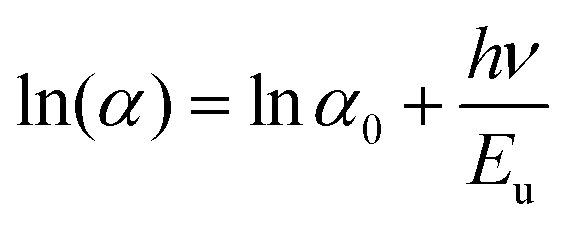
Negative photoconductivity (NPC) is an interesting phenomenon occurring in semiconductors. However, there is no consensus about the actual mechanism of the NPC effect. There are reports attributing NPC to enhanced carrier recombination, carrier trapping, scattering25 and photo-assisted oxygen desorption processes, thereby reducing the hole concentration.26 This implies that there should be enough density of electronic states that can trap the photo-excited charge carrier to avail the NPC. In the case of a molecular system, the structural defects, donor–acceptor levels, charge trapping centres and recombination centres might be abundantly available. These can affect the conductance of the semiconductor and result in NPC. The trapping centres can take away electrons that are excited by the high energy photons. Even though there are many reports on the NPC effect in oxides, chalcogenides, conventional semiconductors, doped hybrid perovskites, monolayer MoS2, and nanowires, there is not much literature available on NPC in devices based on organic molecules. Even though the precise mechanism of the negative photoconductivity (NPC) could be debated, there is consensus on the various mechanisms responsible for this effect. Factors such as enhanced majority carrier recombination, illumination activated defect states that capture the electrons, deep defect states (DX-states) created due to lattice distortion evidenced by the presence of extended Urbach energy, and interaction with the adsorbed molecules have been proposed.27
Negative photoconductivity (NPC) and optical quenching are some of the unusual phenomena shown by the photosensitive materials when illuminated by light.10,21,28–35 The NPC effect has potential uses in optoelectronic memory, optoelectronic switching, optoelectronic detection, gas detection, and other fields.16,36–41 It is useful for extending the capabilities of conventional photoelectric detection and is anticipated to be used with low-power, fast-responding photodetectors.42 Among the photodetectors, UV detectors have been widely used in many fields, such as fire detection, chemical sensing, monitoring of skin exposure, combustion monitoring, forensic application, and security scanning systems, and in radiation dose control in biomedical applications.43–45 Reducing the operational voltage of UV detectors is a challenge. In 2017, a UV detector array with an operational voltage of 1 V was demonstrated using titanium dioxide (TiO2).45 Reduced operational voltage and improved retention of photo-enhanced memristors are highly desired. The photo-enhanced resistive switching technique has the potential to provide substantial advantages in situations calling for long-term endurance and retention, suggesting reliable non-volatile information storage efficiency.
Multilayered organic semiconductor phototransistor memories are shown to be highly stable.46 Organic semiconductors have several advantages over traditional inorganic semiconductors for use as photoactive media, including simplicity of manufacturing, the capacity to create large-area detectors, mechanical flexibility and high absorption coefficient.47 In addition, their frequency response can be tailored to be either wide or narrow.42,48 There have been reports on fullerene-free organic photodetectors (OPDs) that use solution processable indigo as the electron acceptor mixed with the poly(3-n-hexylthiophene) (P3HT) donor.42 Indigo films were also shown to have outstanding stability against air deterioration. The ambipolar dye indigo, which is obtained naturally, has been discovered to have a balanced electron and hole mobility of 1 × 10⁻² cm2 V−1 s−1, which is highly desirable for electronic devices.49 In our previous work, it is established that indigo has a 1.9 eV optical bandgap and exhibits neuromorphic properties including learning and forgetting.50
This work extends the research into the way ultraviolet (UV) light and blue light (BL) affect the function of an indigo–aluminium-based symmetric lateral memristor. A reliable and effective device is constructed using a straightforward method of depositing the prepared solution onto a prefabricated electrode through drop casting, subsequently undergoing annealing for stabilization. This approach ensures both efficiency and stability in the fabrication process, making it a feasible and accessible technique for device production. In addition to its commendable and reliable memory storage capabilities, the device demonstrates the NPC effect. It exhibits heightened photosensitivity to UV light, revealing a photo-enhanced memory window. This study highlights the potential for integrating photodetector and memory storage functionalities for neuromorphic applications.
1 Experimental
The effect of UV and blue light on the Al/indigo/Al device has been studied and the photo-enhanced memory window has been investigated. Indigo (chemical structure displayed in Fig. S1a in the ESI†) is ultrasonicated and stirred in DMSO solvent to form a 0.152 M solution, which is drop cast (2 drops, each drop of 3 μL) using a micropippete on prefabricated inter-digitated aluminium electrodes of gap 125 μm. The UV-vis spectra show very good absorbance (Fig. S1b in the ESI†) in the range of 350 nm to 500 nm, prompting us to use LEDs in this range. We use 375 nm and 475 nm LEDs for all our experiments as light sources. The interdigitated electrodes were found to have an effective conduction length of 2 mm and a breadth of 6 mm, resulting in a total effective area of 12 mm2. The electrode thickness was measured as 11 μm using the Dxt-surface profile measuring system as shown in Fig. S2a in the ESI.† The substrate had a thickness of 0.6 mm. The concentration and volume of the indigo solution were determined through iterative experimentation aimed at achieving a visually uniform layer. This process involved trial and error to optimize both the concentration and volume for effective drop-casting onto the electrodes. The device has been annealed at 100 °C. This simple technique can be used to fabricate an efficient and stable device at room temperature. The I–V characteristics are studied using a Keysight B2902B source meter. Two LEDs of wavelength 375 nm and 475 nm (Intelligent LED solutions) are used to study the effect of photons on the fabricated device.2 Results and discussion
Before exploring the capabilities of the fabricated device, it is important to know the best operational voltage range. As shown in Fig. 1a and b, I–V curves show typical analog type switching, in which a gradual change in the resistance with a small on/off ratio is observed. This kind of analog switching is useful for multi-level memory applications. Fig. 1a and b show the changes in the switching window depending on a series of SET and RESET voltage ranges. In the case of RESET operation as shown in Fig. 1a, the device is investigated by slowly increasing the RESET voltage, but keeping constant the SET voltage, which sets the device to the on state. Similarly, in the case of SET operation, the device is RESET at a constant negative voltage, with increasing SET voltages as shown in Fig. 1b. In such cases, the magnitude of the switching window can be defined as the conductance ratio calculated as the ratio between the difference in the LRS and HRS current and read voltage (Vread) and can be written as51| S.W. = (ILRS − IHRS)/Vread | (1) |
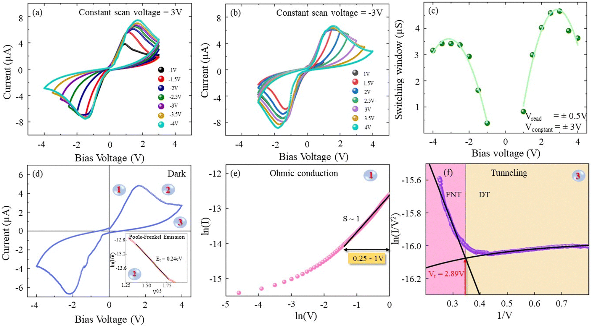 | ||
| Fig. 1 The I–V characteristics of the Al/indigo/Al device under dark conditions, at room temperature and the corresponding conduction mechanisms. (a) I–V measurements for increasing SET stop voltage (negative bias) and repeated RESET cycles (+3 V). (b) Varying the RESET (positive bias) voltage with constant SET (negative voltage) bias (−3 V). (c) Switching window along both voltage directions. (d) A typical hysteresis curve of a memristor with NDR. The positive quadrant is divided into three regions as indicated for further analysis. (inset) The region 2 showing Poole–Frenkel emission and the obtained trap energy is 0.24 eV. (e) Plot of ln(I) vs. ln(V) in the region 1 (from Fig. 1d) shows ohmic conduction. (f) ln(I/V2) vs. (1/V) in the region 3 shows the Fowler–Nordheim tunneling and direct tunneling. The transition voltage is Vt = 2.89 V. | ||
The representation of the current–voltage characteristics in region-2, displayed on a logarithmic scale ln(I/V) versus V0.5, illustrates the phenomenon of Poole–Frenkel (PF) emission. This emission mechanism is accountable for the negative differential resistance (NDR), as depicted in the inset of Fig. 1d. Here, the electrons are thermally excited from the traps to the LUMO of indigo. Consider an electron in a trap centre. An applied electric field across the thin film can lower the electron's Coulomb potential energy. The likelihood that an electron will be thermally excited out of the trap and into the LUMO may increase because of the decrease in Coulomb potential energy. This conduction mechanism is frequently seen at high electric fields because Poole–Frenkel emission is caused by thermal activation under an electric field. The trap energy is obtained as 0.24 eV, calculated from the intercept of the P–F plot (ϕT = Yintercept × kT). The details of trap energy calculation are included in the ESI.† In region-3, the conduction mechanism is distinctly characterized by tunneling, particularly transitioning to Fowler–Nordheim tunneling at higher bias voltages. These two mechanisms compete each other with respect to the applied electric field. At a given bias voltage, the low voltage tunneling will be overcome by the Fowler–Nordheim tunneling, which is depicted as transition voltage (Vt). In the case of our device, the transition occurs at a bias voltage of ∼2.89 V.
A plot of ln(I/V2) vs. (1/V) of the HRS state clearly depicts that it is dominated by the tunnelling conduction mechanism (Fig. (1f)). In the higher voltage region, it is linear, which clearly points the presence of Fowler–Nordheim (FN) tunnelling. The non-pinching of I–V characteristics, NDR and the scan rate dependency of NDR has been explained in our previous work on the Al/indigo/Al device.50 Up to 1.64 V the current increases with bias voltage due to ohmic conduction. After that a reduction in current can be seen where Poole–Frenkel emission happens. The majority carriers responsible for the conduction get trapped in the trap sites of indigo, which results in the reduction of current. While sweeping back from higher voltages to lower voltages, the trapped charge carriers will encounter a thinner barrier and will undergo F–N tunnelling up to 2.89 V. At a lower bias voltage, charge carriers start to encounter the full barrier height and a smaller number of charge carriers undergo direct tunnelling, as a result of which conductivity further reduces. It is important to determine the effect of optical illumination on the current–voltage characteristics for using indigo based devices as UV-detectors. With UV light on (375 nm, 0.165 W mm−2), we swept the bias voltage in the range of ± 4 V. As shown in Fig. 2a hysteric I–V characteristics are observed almost similar to the I–V characteristics recorded without any light illumination (refer Fig. 1a) with a reduction in overall current by a factor of 2. Most importantly, the NDR behaviour has disappeared. Once the effect of 375 nm light has been studied in detail, I–V characteristics using blue light (475 nm, a power density of 0.165 W mm−2) are also studied. Interestingly, both hysteresis and NDR have completely disappeared. The current further decreased by a factor of 10 from the previous state, which is depicted in Fig. 2b. The ln(I)–ln(V) plot depicts the ohmic conduction mechanism present in the LRS. Similar to dark conditions, Fowler–Nordheim (FN) tunnelling and direct tunnelling are responsible for the HRS conduction mechanism under UV illumination, as shown in the inset of Fig. 2d. However, under blue light illumination, conduction further reduced and direct tunnelling of electrons dominated in the HRS. The analysis of ln(I/V) vs. V0.5 reveals the location of trap states above the LUMO of the indigo molecule. From the analysis of I–V curves in the dark and under 375 nm and 475 nm light, we propose the NPC mechanism occurring in the indigo as shown in Fig. 3e. In the case of indigo molecules, the HOMO–LUMO gap is 1.9 eV obtained via UV-vis spectroscopy.50 This means that the resonant excitation takes place when the photon energy exactly matches with the optical energy gap. When the photon energy is more than the optical energy gap, the absorption process generates hot electrons and they can thermally relax to the LUMO edge via electron–electron scattering or electron–phonon scattering, generally termed as thermalisation. When the excitation photon energy is higher than the trap energy levels, then, the hot electrons not only can relax to the LUMO edge, but also can be trapped in these trap states. Trapping of such electrons will temporarily reduce the electron concentration in the LUMO, thus reducing the conductance of the indigo molecular layer. From the analysis of the ln(I/V) vs. V0.5 measured in the dark and under 375 nm and 475 nm light, we find that the trap states are located 0.2–0.4 eV above the LUMO edge.
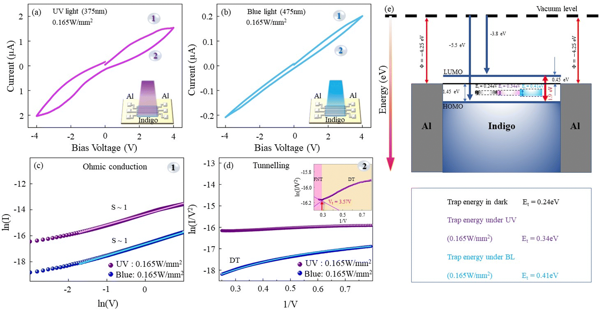 | ||
| Fig. 2 The I–V characteristics of the Al/indigo/Al device under light illumination with 4 V bias, at room temperature and the corresponding conduction mechanisms. The I–V measurement under (a) 375 nm UV illumination and (b) 475 nm blue light illumination. (c) The region 1 shows ohmic conduction for both light sources. (d) The region 2 shows F–N tunnelling and direct tunnelling under UV illumination (zoomed-in figure shown in the inset) and only direct tunnelling under blue light illumination. (e) The band diagram of the Al/indigo/Al device and the change in trap energy under UV and BL illumination with the same intensity of 0.165 W mm−2. | ||
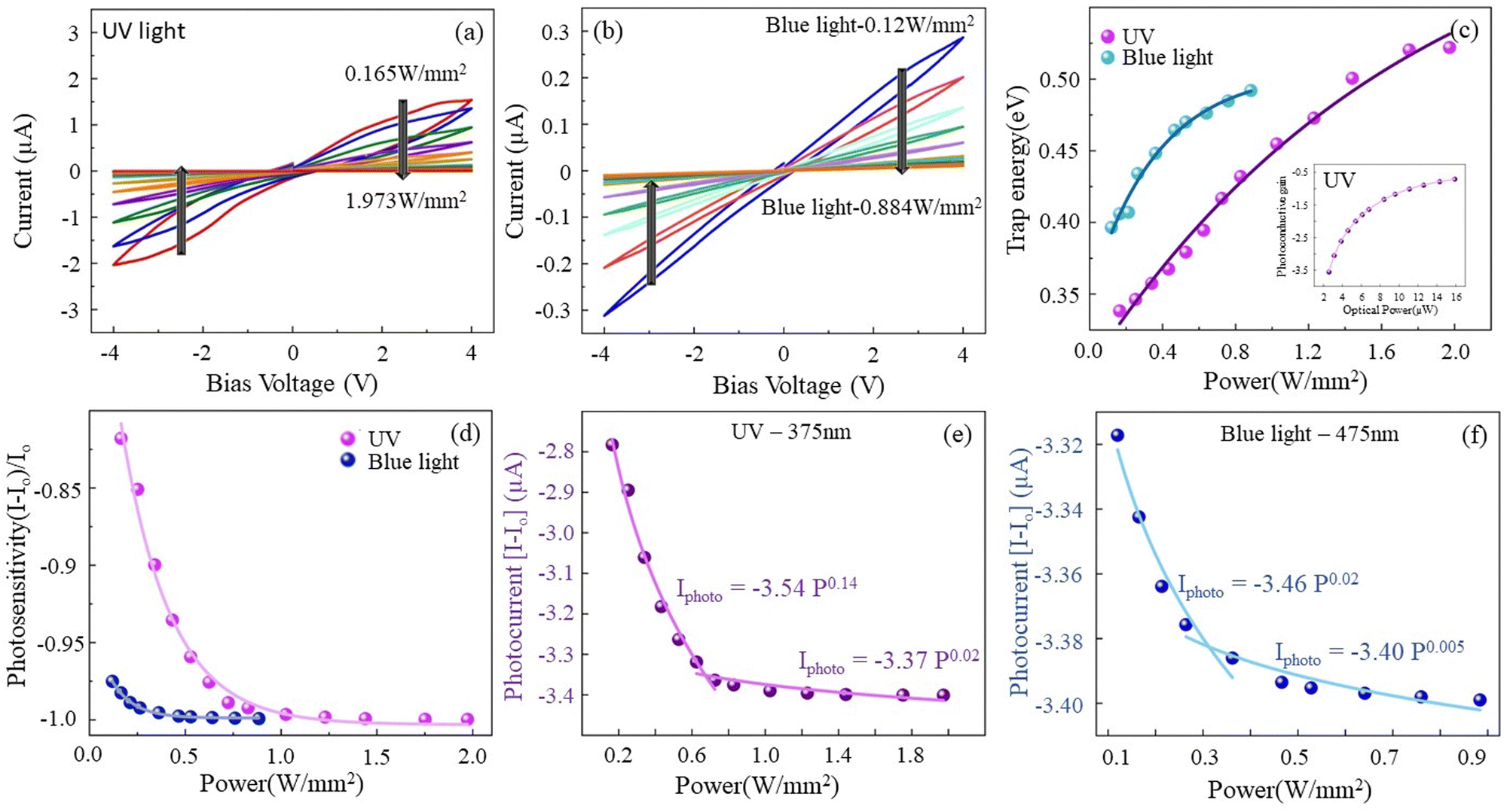 | ||
| Fig. 3 The effect of UV (375 nm) and blue (475 nm) light on I–V characteristics and photoconductance. (a) Effect of UV light (375 nm) exposure on I–V characteristics. The intensity of light used is mentioned. (b) Reduction in overall current observed during the successive I–V measurements under blue light (475 nm). The intensity of light used is mentioned. (c) The dependence of trap energy on the power density of UV and blue light sources. (c inset) Photoconductive gain of the device with varying optical power of the UV source. (d) The photosensitivity variation with intensity of light. (e) and (f) The power law dependence of photocurrent on power density of UV and blue light respectively. | ||
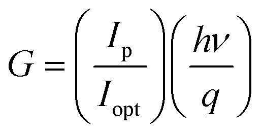
To evaluate the trap energy distribution, the I–V curves are measured by increasing the intensity of the light. Fig. 3(a) and (b) show I–V curves measured under such conditions for UV-light and blue-light respectively. In both cases, we observe a reduction in the overall current. Furthermore, the current is lower by a factor of 5 when exposed to blue light. We consider the systematic reduction of current as a negative photoconductive effect, which causes the total current level of hysteresis to drop as UV and blue light illumination intensity is increased. Each I–V sweep measurement was conducted after exposing the device to the respective light intensity for a specific duration, ensuring that the observed characteristics correspond to the particular intensity under consideration. Using Poole–Frenkel emission (as shown in Fig. S3 in the ESI†), we can estimate the location of the trap by finding out the y-intercept of ln(I/V) versus V0.5. As shown in Fig. 3c, the gradual change in the trap state is calculated, which indicates that the trap states indeed spread over an energy range of about 175 meV, which is about 4–5 times that of the thermal energy corresponding to room temperature. The intensity of the light being used in this case also has a huge effect on the photoresponsivity as shown in Fig. 3d. In general, when light intensity is increased, more and more electron–hole pairs should be generated resulting in the increased photocurrent and electron–hole pairs should be collected at the respective electrodes. In our device, as the light intensity is increased, the generated carriers are more and more captured by the trap states due to impurities and defects within the indigo film and the indigo–glass interface. When light intensity is low, the photo-generated electrons are mostly captured by the trap states effectively reducing the recombination of electron–hole pairs. As the light intensity is increased, a lower number of trap states are available, and hence a relatively lower number of electrons are captured by the trap states, implying more recombination of electron–hole pairs. At both wavelengths of light used, we see a similar trend of the device being more sensitive to lower light intensity. To get a more quantitative understanding of the dependence of photocurrent on the intensity of light, the photocurrent Iphoto = (I − I0) can be plotted against the light intensity and can be fitted using a power law: Iph = A × Pα, where A is the constant, P is the light power used to illuminate the device, and α is the exponent. Similarly, the photoconductive gain (G) can be calculated as
 | (2) |
Fig. 4a presents the transient photo-response of the indigo device. Even though we have seen a negative photo-response in the dc–IV curves, where the device was exposed to UV light for a given duration before conducting I–V measurements, the transient response is quite different. When current is monitored when light is on, initially, we see a positive photo-response. As shown in Fig. 4a, the UV-LED was on (power ∼0.725 W mm−2) for 400 s and then switched off for the same duration with a constant voltage of 1 V applied to the device to monitor the photo-generated current. This on/off cycle is repeated 4 times to check the consistency of the measurements. The current increases to a maximum (Imax = 8.38 nA) in 200 s and after that it starts to decrease exponentially until the UV source is switched off. This exponential decrease before switching off the light source is due to the NPC effect. Even if we think of using shallow donors in the case of indigo molecules, these would contribute to non-zero current without the light pulse.
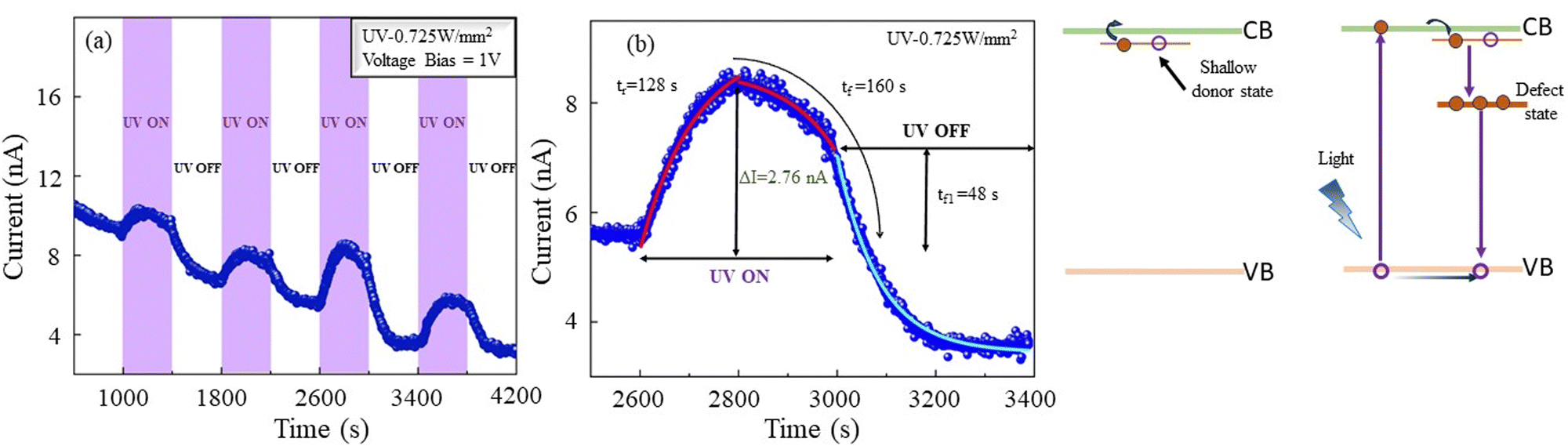 | ||
| Fig. 4 The effect of UV light on the Al/indigo/Al device. (a) Five cycles of UV on/off measurements with a UV light intensity of 0.725 W mm−2. (b) One random cycle of UV on–off measurements with a UV light intensity of 0.725 W mm−2 for detailed analysis of NPC followed by PPC. (c) A schematic diagram of the effect of defect states on capturing the electrons excited due to the exposure to light. | ||
The initial increase in the photo-induced current is due to creation of the electron–hole pairs once the device is exposed to UV-light. While the electrons are excited to the conduction band, the holes are left behind. The generation of electron–hole pairs is a faster process, thus resulting in a positive photoconductivity. As soon as there is appreciable amount of photo-generated charge carriers, the trap centers can start capturing electrons, thus reducing the current measured. We see that the trapping of photo-generated current dominates after a while resulting in reduction of current. Upon turning off the light, the recombination of generated charge carriers increases, leading to an exponentially decaying current. This kind of measurement is helpful to understand the competition between the photoengraved charge carriers and dynamics of trapped electrons in the molecular film. The formation of a special kind of defect state, which limits the carrier density, is well-known. In the case of zinc blende or wurtzite type semiconductors, and doped perovskite crystals, the DX type (or sometimes referred to as the DY-type) type of defect centres are found to trap the electrons. In the case of a bismuth doped Pb perovskite system, the DX centre is a lattice location where the Bi replaces a Pd atom with a small displacement resulting in breaking of three metal–halide bonds resulting in the formation of a DX trap centre.23 The presence of this special trap energy state can be determined by finding out the band tail from the absorption coefficient. For this, we use the Tauc plot to check if there is an extended band tail near the band edge, indicating an increased amount of defect states as follows:
 | (3) |
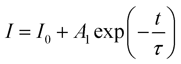
To further analyse the dynamics of the rise and decay processes, we consider the third cycle from Fig. 4a. The interplay of these opposing factors governs the overall conductivity of the device. The rise and fall of the current after switching off the light source can be fitted by a double exponential equation as:
 | (4) |
To check the device performance in terms of the memory states and the effect of UV light on the memory states, well established read–write–read–erase–read (RWRER) voltage cycles have been applied to the devices. Fig. 5 shows results of such measurements. Fig. 5a shows the typical voltages applied during the RWRER cycles and the corresponding current levels measured are also shown. We apply ±4 V as write-pulse and erase pulse and the current levels are measured at 0.9 V. These measurement parameters are chosen on the basis of the DC current–voltage measurements as indicated in Fig. 1d. We obtain non-zero crossing current–voltage characteristics and up to 0.63 V in the first quadrant, we have negative current. Thus, we have selected a slightly higher value of read voltage of 0.9 V so as to get a clear high resistance state and low resistance state. The details are shown in Fig. S2b and c (ESI†). The existence of two current states is indicated by a yellow bar in Fig. 5a. The high stability of memory characteristics is evidenced by the endurance of 9000 cycles with increasing memory window (ΔR ∼ 2.3 MΩ at the 1000th cycle increased to 4.1 MΩ at the 8500th cycle) as shown in Fig. 5b. This stable two-state memory is stable up to ∼1 hour as shown in Fig. 5c, supporting the high stability of the molecular device. Interestingly, the UV exposure improved the two-resistance state performance of this device. The memory window increased from 1.8 MΩ at the 100th cycle in the dark to 2.42 MΩ upon exposure to UV radiation of intensity 0.165 W mm−2 (Fig. 5e). When the intensity is increased to 0.528 W mm−2 (as shown in Fig. 5f) the memory window further increased to 3.39 MΩ. This change in clearly indicated in Fig. S5 (ESI†), where the change ΔR is plotted for the above three cases. Here, ΔR is the difference between the HRS state and LRS state. Clearly upon exposure to UV light, the device becomes more and more stable and the resistance states become more and more stable.
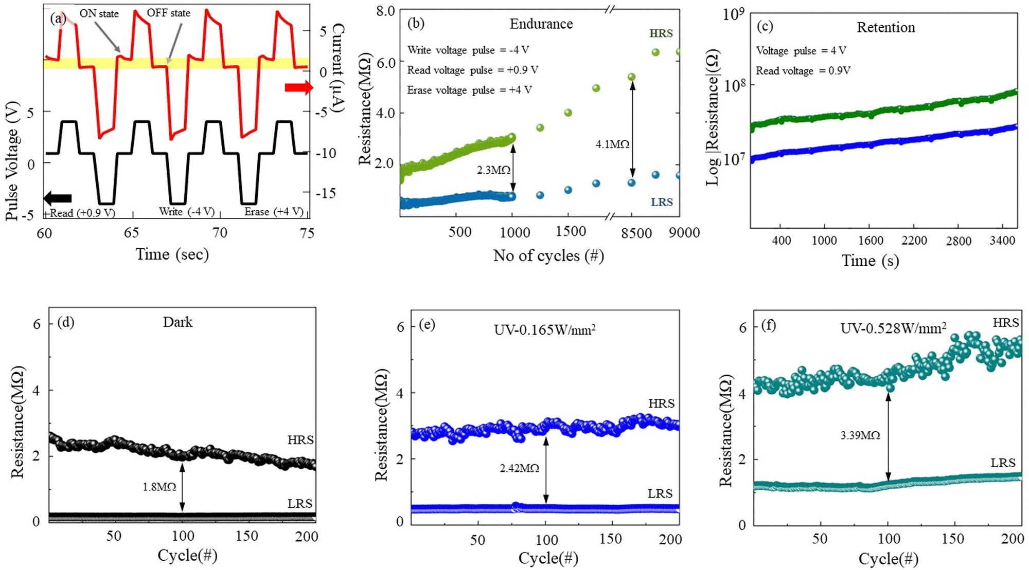 | ||
| Fig. 5 The read–write–erase cycles and memory window. (a) Read–write–erase voltage pulses (black line), Vread = 0.9 V, Vwrite = −4 V, Verase = 4 V; the corresponding current indicated by a red line. (b) Endurance up to 9000 cycles shown (Vread = 0.9 V, Vwrite = −4 V, Verase = 4 V). (c) Retention characteristics of the device (voltage pulse = 4 V & 2 V, read voltage = 0.9 V). The memory window (d) in the dark and (e) upon exposure to UV radiation with intensities of 0.165 W mm−2 (f) and 0.528 W mm−2. | ||
3 Conclusions
We have demonstrated the potential of the Al/indigo/Al device to combine the highly desirable functions such as efficient UV photodetection, data processing, and data storage along with the UV enhanced memory window. From the switching window measurements, the operational voltage (Vo) for synaptic operations is found to be 1 V < Vo < 3 V. The conduction mechanisms under dark conditions and under UV and blue light illumination are analysed. It is found that the fabricated molecular based device is more sensitive to UV illumination. The negative photoconductive effect (NPC) effect is attributed to oxygen adsorption and desorption processes, which affect the overall concentration of charge carriers. The indigo device also shows an enhanced memory window under UV illumination. The power law suggests that strong electron–hole recombination takes place in the device with increase in the intensity of illumination. The increased trap energy with increased intensity of illumination enhanced the NPC effect. The sensitivity towards UV illumination is further explored by photoconductive gain calculations and photo-response analysis along with UV on–off measurements. Our work highly recommends this naturally sourced indigo dye molecule for UV detection applications. The response time can be improved by doping.Author contributions
B. S.: conceptualization, data curation, formal analysis, investigation, visualization, writing – original draft, writing – reviewing and editing; R. T.: conceptualization, methodology, project administration, resources, supervision, validation, writing – reviewing and editing.Conflicts of interest
The authors declare that there are no conflicts of interest.Acknowledgements
B. S. and R. T. would like to thank the Centre for Functional Materials (CFM), Vellore Institute of Technology for their support during this research work. R. T. would like to acknowledge the Core Research Grant (CRG/2022/005093) from the Science and Engineering Board (SERB), India.References
- H. Tan, G. Liu, H. Yang, X. Yi, L. Pan, J. Shang, S. Long, M. Liu, Y. Wu and R. Li, Light-Gated Memristor with Integrated Logic and Memory Functions, ACS Nano, 2017, 11, 11298 CrossRef CAS PubMed.
- J. Mao, L. Zhou, X. Zhu, Y. Zhou and S. Han, Photonic memristor for future computing: a perspective, Adv. Opt. Mater., 2019, 7(22), 1900766 CrossRef CAS.
- J. Zhao, Z. Zhou, H. Wang, J. Wang, W. Hao, D. Ren, R. Guo, J. Chen, B. Liu and X. Yan, A Boolean OR gate implemented with an optoelectronic switching memristor, Appl. Phys. Lett., 2019, 115(15), 153504 CrossRef.
- S. Cai, C. Tzou, Y. Liou, D. Chen, C. Jiang, J. Ma, C. Chang, C. Tseng, Y. Liao, Y. Hsieh, M. Hofmann and Y. Chen, Hybrid Optical/Electric Memristor for Light-Based Logic and Communication, ACS Appl. Mater. Interfaces, 2019, 11(4), 4649 CrossRef CAS PubMed.
- X. Shan, C. Zhao, X. Wang, Z. Wang, S. Fu, Y. Lin, T. Zeng, X. Zhao, H. Xu, X. Zhang and Y. Liu, Plasmonic Optoelectronic Memristor Enabling Fully Light-Modulated Synaptic Plasticity for Neuromorphic Vision, Adv. Sci., 2022, 9(6), 2104632 CrossRef CAS PubMed.
- P. Maier, F. Hartmann, M. Emmerling, C. Schneider, M. Kamp, S. Höfling and L. Worschech, Electro-photo-sensitive memristor for neuromorphic and arithmetic computing, Phys. Rev. Appl., 2016, 5(5), 054011 CrossRef.
- Z. Zhou, Y. Pei, J. Zhao, G. Fu and X. Yan, Visible light responsive optoelectronic memristor device based on CeOx/ZnO structure for artificial vision system, Appl. Phys. Lett., 2021, 118(19), 191103 CrossRef CAS.
- S.-L. Gao, L.-P. Qiu, J. Zhang, W.-P. Han, S. Ramakrishna and Y.-Z. Long, Persistent Photoconductivity of Metal Oxide Semiconductors, ACS Appl. Electron. Mater., 2024, 6(3), 1542 CrossRef CAS.
- A. Sumanth, K. Lakshmi Ganapathi, M. S. Ramachandra Rao and T. Dixit, A review on realizing the modern optoelectronic applications through persistent photoconductivity, J. Phys. D: Appl. Phys., 2022, 55(39), 393001 CrossRef CAS.
- S. G. Cho, T.-U. Nahm and E. K. Kim, Deep level states and negative photoconductivity in n-ZnO/p-Si hetero-junction diodes, Curr. Appl. Phys., 2014, 14(3), 223 CrossRef.
- L. Lu, X. Jiang, H. Peng, D. Zeng and C. Xie, Quantitative characterization of the long-term charge storage of a ZnO-based nanorod array film through persistent photoconductance, RSC Adv., 2018, 8(30), 16455 RSC.
- S. Cai, G. Parish, J. M. Dell and B. D. Nener, Contribution of hole trap to persistent photoconductivity in n-type GaN, J. Appl. Phys., 2004, 96(2), 1019 CrossRef CAS.
- S. Kaushik, A. K. Kapoor, R. K. Pant, S. B. Krupanidhi and R. Singh, Observation of negative photoconductivity at bandgap and super bandgap excitations in GaN nanorods, Opt. Mater., 2021, 121, 111553 CrossRef CAS.
- Y. C. Lee, J. L. Shen, K. W. Chen, W. Z. Lee, S. Y. Hu, K. K. Tiong and Y. S. Huang, Observation of persistent photoconductivity in 2H-MoSe2 layered semiconductors, J. Appl. Phys., 2006, 99(6), 063706 CrossRef.
- Chandan, S. Sarkar and B. Angadi, Defects induced persistent photoconductivity in monolayer MoS2, Appl. Phys. Lett., 2021, 118(17), 172105 CrossRef CAS.
- C. H. Lui, A. J. Frenzel, D. V. Pilon, Y. H. Lee, X. Ling, G. M. Akselrod, J. Kong and N. Gedik, Trion-Induced Negative Photoconductivity in Monolayer MoS2, Phys. Rev. Lett., 2014, 113(16), 166801 CrossRef CAS PubMed.
- J. K. Gustafson, D. Wines, E. Gulian, C. Ataca and L. M. Hayden, Positive and Negative Photoconductivity in Monolayer MoS2 as a Function of Physisorbed Oxygen, J. Phys. Chem. C, 2021, 125(16), 8712 CrossRef CAS.
- E. Song, W. Si, R. Cao, P. Feng, I. Mönch, G. Huang, Z. Di, O. G. Schmidt and Y. Mei, Schottky contact on ultra-thin silicon nanomembranes under light illumination, Nanotechnology, 2014, 25(48), 485201 CrossRef PubMed.
- S. Paramanik and A. J. Pal, Combining negative photoconductivity and resistive switching towards in-memory logic operations, Nanoscale, 2023, 15(10), 5001 RSC.
- Y. Han, M. Fu, Z. Tang, X. Zheng, X. Ji, X. Wang, W. Lin, T. Yang and Q. Chen, Switching from Negative to Positive Photoconductivity toward Intrinsic Photoelectric Response in InAs Nanowire, ACS Appl. Mater. Interfaces, 2017, 9(3), 2867 CrossRef CAS PubMed.
- A. Grillo, E. Faella, A. Pelella, F. Giubileo, L. Ansari, F. Gity, P. K. Hurley, N. McEvoy and A. Di Bartolomeo, Coexistance of Nagative and Positive photoconductivity in few layer PtSe2 Field effect transistors, Adv. Funct. Mater., 2021, 31(43), 2105722 CrossRef CAS.
- K. Ikeda, D. Yoo, R. Nishikawa, T. Kawamoto and T. Mori, Charge injected proton transfer in indigo derivatives, Phys. Chem. Chem. Phys., 2021, 23(38), 21972 RSC.
- M. A. Haque, J. L. Li, A. L. Abdelhady, M. I. Saidaminov, D. Baran, O. M. Bakr, S. H. Wei and T. Wu, Transition from Positive to Negative Photoconductance in Doped Hybrid Perovskite Semiconductors, Adv. Opt. Mater., 2019, 7(22), 1900865 CrossRef CAS.
- J. An, G. Chen, X. Zhu, X. Lv, J. Bao and X. Xu, Ambipolar Photoresponse of CsPbX3–ZnO (X = Cl, Br, and I) Heterojunctions, ACS Appl. Electron. Mater., 2022, 4(4), 1525 CrossRef CAS.
- P. C. Wei, S. Chattopadhyay, M. D. Yang, S. C. Tong, J. L. Shen, C. Y. Lu, H. C. Shih, L. C. Chen and K. H. Chen, Room-temperature negative photoconductivity in degenerate InN thin films with a supergap excitation, Phys. Rev. B: Condens. Matter Mater. Phys., 2010, 81(4), 045306 CrossRef.
- Y. Yang, X. Peng, H. S. Kim, T. Kim, S. Jeon, H. K. Kang, W. Choi, J. Song, Y. Doh and D. Yu, Hot Carrier Trapping Induced Negative Photoconductance in InAs Nanowires toward Novel Nonvolatile Memory, Nano Lett., 2015, 15(9), 5875 CrossRef CAS PubMed.
- Y. Wang, Z. He, J. Zhang, H. Liu, X. Lai, B. Liu, Y. Chen, F. Wang and L. Zhang, UV illumination enhanced desorption of oxygen molecules from monolayer MoS2 surface, Nano Res., 2020, 13(2), 358 CrossRef CAS.
- V. S. Vavilov, Effects of Radiation on Semiconductors, Springer, New York, 2013, vol. 1 Search PubMed.
- J. R. Barrett and G. C. Gerhard, Negative Photoconductivity in Gold-Doped Silicon, J. Appl. Phys., 1967, 38(2), 900 CrossRef CAS.
- N. K. Tailor, P. Maity, M. I. Saidaminov, N. Pradhan and S. Satapathi, Dark Self-Healing-Mediated Negative Photoconductivity of a Lead-Free Cs3Bi2Cl9 Perovskite Single Crystal, J. Phys. Chem. Lett., 2021, 12(9), 2286 CrossRef CAS PubMed.
- W. Schneider, Theory of the Negative Photoconductivity in Crossed Fields, Appl. Phys., 1976, 11(2), 141 CAS.
- V. Ryzhii, M. Ryzhii, D. S. Ponomarev, V. G. Leiman, V. Mitin, M. S. Shur and T. Otsuji, Negative Photoconductivity and Hot Carrier Bolometric Detection of Terahertz Radiation in Graphene Phosphorene Hybrid Structures, J. Appl. Phys., 2019, 125(15), 151608 CrossRef.
- J. Jayabharathi, A. Prabhakaran, C. Karunakaran, V. Thanikachalam and M. Sundharesan, Structural, optical and photoconductivity characteristics of pristine FeO. Fe2O3 and NTPI-FeO. Fe2O3 nanocomposite: aggregation induced emission enhancement of fluorescent organic nanoprobe of thiophene appended phenanthrimidazole derivative, RSC Adv., 2016, 6(22), 18718 RSC.
- H. Wang, et al., Slowing Hot-Electron Relaxation in Mix-Phase Nanowires for Hot-Carrier Photovoltaics, Nano Lett., 2021, 21(18), 7761 CrossRef CAS PubMed.
- Y. Liu, P. Fu, Y. Yin, Y. Peng, W. Yang, G. Zhao, W. Wang, W. Zhou and D. Tang, Positive and Negative Photoconductivity Conversion Induced by H2O Molecule Adsorption in Wo3 Nanowire, Nanoscale Res. Lett., 2019, 14(144), 1 Search PubMed.
- D. Alvarenga, C. A. Parra-Murillo, G. M. Penello, R. Kawabata, W. N. Rodrigues, D. R. Miquita, W. Schmidt, P. S. S. Guimaraes, M. P. Pires, K. Unter-rainer and P. L. Souza, Simultaneous positive and negative photocurrent response in asymmetric quantum dot infrared photodetectors, J. Appl. Phys., 2013, 113(4), 043721 CrossRef.
- C. Yang, T. Chen, D. Verma, L. Li, B. Liu, W. Chang and C. Lai, Bidirectional All-Optical Synapses Based on a 2D Bi2O2 Se/Graphene Hybrid Structure for Multifunctional Optoelectronics, Adv. Funct. Mater., 2020, 30(30), 2001598 CrossRef CAS.
- M. Y. Hassan and D. S. Ang, On-Demand Visible-Light Sensing with Optical Memory Capabilities Based on an Electrical-Breakdown-Triggered Negative Photoconductivity Effect in the Ubiquitous Transparent Hafnia, ACS Appl. Mater. Interfaces, 2019, 11(45), 42339 CrossRef CAS PubMed.
- K. Nese, A. K. Sertap and O. Sener, Observation of negative photoconductivity in (ZnO)x (CdO)1−x films, J. Phys. Chem. Solids, 2009, 70(3), 521 Search PubMed.
- A. S. Chaves and H. Chacham, Negative photoconductivity in semiconductor heterostructures, Appl. Phys. Lett., 1995, 66(6), 727 CrossRef CAS.
- G. Kim, I. G. Kim, J. H. Baek and O. K. Kwon, Enhanced frequency response associated with negative photoconductance in an InGaAs/InAlAs avalanche photodetector, Appl. Phys. Lett., 2003, 83(6), 1249 CrossRef CAS.
- I. K. Kim, X. Li, M. Ullah, P. E. Shaw, R. Wawrzinek, E. B. Namdas and S. C. Lo, Fullerene-Free Organic Photodiodes Based on a Solution-Processable Indigo, Adv. Mater., 2015, 27, 6390 CrossRef CAS PubMed.
- P. Cheong, K. Chang, Y. Lai, S. Ho, I. Sou and K. Tam, A ZigBee-based wireless sensor network node for ultraviolet detection of flame, IEEE Trans. Ind. Electron., 2011, 58(11), 5271 Search PubMed.
- M. Razeghi and A. Rogalski, Semiconductor ultraviolet detectors, J. Appl. Phys., 1996, 79(10), 7433 CrossRef CAS.
- M. Cesarini, M. Binda and D. Natali, Printable UV detector arrays based on light-induced conductance switching in mesoporous titanium dioxide, Org. Electron., 2017, 49, 100 CrossRef CAS.
- T. T. Dao, H. Sakai, K. Ohkubo, S. Fukuzumi and H. Murata, Low switching voltage, high-stability organic phototransistor memory based on a photoactive dielectric and an electron trapping layer, Org. Electron., 2020, 77, 1566 CrossRef.
- W. Brütting, Introduction to the Physics of Organic Semiconductors, Phys. Org. Semicond., 2005, 1, 1 Search PubMed.
- A. Armin, V. R. D. Jansen-van, N. Kopidakis, P. L. Burn and P. Meredith, Nat. Commun., 2015, 6, 6343 CrossRef CAS PubMed.
- I. V. Klimovich, A. V. Zhilenkov, L. I. Kuznetsova, L. A. Frolova, O. R. Yamilova, S. I. Troyanov, K. A. Lyssenko and P. A. Troshin, Novel functionalized indigo derivatives for organic electronics, Dyes Pigm., 2021, 186, 108966 CrossRef CAS.
- B. Sreelakshmi and R. Thamankar, Coexistence of synaptic behaviour and negative differential resistance at room temperature in the resistive switching device based on natural indigo molecules, Dyes Pigm., 2023, 219, 111638 CrossRef CAS.
- S. Bang, M. H. Kim, T. H. Kim, D. K. Dong Keun Lee, S. Kim, S. Cho and B. G. Park, Gradual switching and self-rectifying characteristics of Cu/α-IGZO/p+-Si RRAM for synaptic device application, Solid-State Electron., 2018, 150, 60 CrossRef CAS.
- L. Shen, S. Yip, C. Lan, L. Shu, D. Li, Z. Zhou, C. Wong, E. Y. B. Pun and J. Ho, Enhanced Negative Photoconductivity in InAs Nanowire Phototransistors Surface-Modified with Molecular Monolayers, Adv. Mater. Interfaces, 2018, 5, 1701104 CrossRef.
- M. Garg, B. R. Tak, V. R. Rao and R. Singh, Giant UV Photoresponse of GaN-Based Photodetectors by Surface Modification Using Phenol-Functionalized Porphyrin Organic Molecules, ACS Appl. Mater. Interfaces, 2019, 11, 12017 CrossRef CAS PubMed.
- C. Kaiser, O. J. Sandberg, N. Zarrabi, W. Li, P. Meredith and A. Armin, A universal Urbach rule for disordered organic semiconductors, Nat. Commun., 2021, 12(1), 3988 CrossRef CAS PubMed.
- C. Zhang, S. Mahadevan, J. Yuan, J. K. W. Ho, Y. Gao, W. Liu, H. Zhong, H. Yan, Y. Zou, S. Tsang and S. K. So, Unraveling Tail Effects in High-Performance Organic Photovoltaics: Dynamic vs Static Disorder, ACS Energy Lett., 2022, 7(6), 1971 CrossRef CAS.
Footnote |
| † Electronic supplementary information (ESI) available. See DOI: https://doi.org/10.1039/d4ma00302k |
| This journal is © The Royal Society of Chemistry 2024 |