
 Open Access Article
 This Open Access Article is licensed under a
 Creative Commons Attribution 3.0 Unported Licence
Variability of Cu2ZnSnS4 nanoparticle hot injection synthesis and modifications by thin film annealing
K. P.
Stroh†
 ,
M.
Szablewski
and
D. P.
Halliday
*
,
M.
Szablewski
and
D. P.
Halliday
*
Department of Physics, Durham University, South Road, Durham, UK DH1 3LE. E-mail: d.p.halliday@durham.ac.uk; marek.szablewski@durham.ac.uk
First published on 20th October 2023
Abstract
As a quaternary semiconductor with a direct energy bandgap of around 1.4 eV, Cu2ZnSnS4 is a promising candidate for absorber layers in next generation thin-film solar PV devices. It has the advantage of being based on low cost earth-abundant elements. Solution based synthesis approaches show the greatest potential for scaling up manufacture. Cu2ZnSnS4 devices are currently limited in efficiency because of a large open circuit voltage deficit, arising predominantly from high concentrations of point defects and charge compensation defect complexes. To drive device efficiency robust, reliable and reproducible synthesis protocols are required. We have produced a series of Cu2ZnSnS4 thin films by spin coating nanoparticle ink suspensions fabricated under nominally identical conditions to investigate the inherent variability in hot injection synthesis of Cu2ZnSnS4 nanoparticles by fabricating 11 batches using the same initial conditions. We use two different chemical routes to extratct nanoparticles from solution after synthesis. We find that the lattice constants of the nanocrystalline material do not change significantly. The relative concentration of the constituent elements varies with S having the largest anion variation of ±3.8% as compared to metal cation variations of Zn ±2.4%, Cu ±1.8%, and Sn ±1.4% with Zn having the largest cation variation. We compare data from energy dispersive X-ray (EDX) and inductively coupled plasma mass spectroscopy (ICPMS) chemical analysis methods and find that the ICPMS analysis has a consistently smaller standard deviation, an average of 0.1 lower, as this technique samples a large volume of material. We observe variation in the kesterite tetragonal lattice constants a and c, and energy bandgap Eg across the different samples, although there is no systematic change in the chemical composition. The average bandgap of as-synthesised films is 1.14 eV. We find that annealing in a sulphur rich environment has no systematic impact on the Cu/(Zn + Sn) cation ratio and leads to a decrease of −0.4 in the Zn/Sn ratio. At higher annealing temperatures, 500–600 °C, the bandgap shows a linear increase of +0.15 eV accompanied by the formation of abnormal grains and an increase in the size of the crystalline scattering domain τ, determined from the X-ray spectra, from 30–100 nm. The most dramatic changes occur in the first 0.5 hours of annealing. These findings will help in the design of fabrication strategies for higher efficiency Cu2ZnSnS4 photovoltaic devices.
Introduction
Alternatives for the next generation of suitable semiconductor materials for future thin-film solar cells are under active exploration.1 With a focus on low cost and earth-abundant elements, Cu2ZnSnS4 (CZTS) has been identified as a promising contender.2 However, efficiencies of CZTS devices are currently limited because of the large open circuit voltage deficit.3 As a quaternary semiconductor system, CZTS has a large number of native point defects and charge-compensating defect complexes which alter the energy bandgap, and modify carrier dynamics and PV device behaviour.4,5 Common defects include CuZn and ZnCu antisites where associated electrostatic potential fluctuations can reduce the energy bandgap.6,7 These charge-compensating defect complexes have been found to determine the overall crystal structure and composition of CZTS limiting the composition to specific parts of the compositional phase diagram.8,9 Since its development by Guo et al.,10 the hot injection method for synthesising CZTS films via intermediate nano-crystalline ink deposition has become a predominant method for the facile synthesis of CZTS thin films.11Currently CZTS devices have efficiencies of 10%2 with the scope for further improvement.3 A key aspect of further enhancing device efficiency is effective control over fabrication routes to produce materials of known composition, stoichiometry, and doping level.12,13 As a solution-based method, the hot injection process has inherent variability. Changes to the fabrication route have improved overall device efficiency but considerable opportunity for improvement remains. Although the hot-injection process is commonly used, there has been little systematic investigation of the variability and reproducibility of the synthesis process, and the impact of post synthesis annealing under a sulphur atmosphere. In this work, we report on a systematic investigation to establish the variability and reproducibility of the hot injection process by investigating structural, chemical, and electronic properties of 11 batches of CZTS nanocrystalline inks, and related spin coated thin films, fabricated by hot injection using the same parameters in each case. We further investigate the impact of post deposition annealing of thin films in a sulphur-rich environment. Overall, this work presents a careful, systematic report of the inherent variability of the CZTS hot injection synthesis process, and the impact on key material properties. These findings represent a significant advance in our understanding of the impact of hot injection synthesis and subsequent annealing on CZTS material parameters relevant to PV device operation. This will enable growth and thermal processing strategies to be developed that can control the key properties to enhance PV device performance. For further details see the thesis by Stroh.14
Synthesis and analysis methods
Nanocrystal ink synthesis
The precursors used for the CZTS synthesis were copper(II) acetylacetonate (99.99%), zinc acetylacetonate (99.995%) and tin(IV) bis(acetylacetonate) dichloride (98%). All powders were used as supplied by Sigma Aldrich; we quote the manufacturer's level of purity. Our investigation was based on the approach adopted by Guo et al.15 using 1.332 mmol Cu precursor, 0.915 mmol Zn precursor and 0.75 mmol Sn precursor (corresponding to 348.7 mg, 241.2 mg, and 290.9 mg, respectively) with the intention of fabricating Cu-poor and Zn-rich materials known to produce more efficient PV devices.16 Amounts were weighed to a precision of 0.1 mg. The molar ratio of the as-synthesised nanocrystalline inks will differ from the precursor ratio as they are not incorporated into the growing particles at the same rates. To produce CZTS, an excess of elemental sulphur (4 mmol) dissolved in oleylamine was added. The procedure we used has been described in detail previously.17 Our synthesis temperature, when sulphur is injected, was 225 °C.For washing, centrifugation, and collection of the synthesised nanoparticles, two approaches were used. For samples S01–S04 a toluene–isopropanol regime was used to collect the nanoparticles for centrifugation after synthesis, as originally described by Guo et al.10 For samples S05–S11 an alternative nanoparticle collection regime was used based on ethanol, hexane and isopropanol following the later approach adopted by Guo et al.15 This second approach also uses hexanethiol as the nanoparticle solvent for spin coating. We find that there is no systematic difference in as-synthesised CZTS nanocrystal material properties between these two routes. However, we do find that the efficiency of nanoparticle collection, and the overall quality and reproducibility of spin-coated thin-films is enhanced using the second regime. Using the ethanol, hexane and isopropanol regime consistently delivered a greater amount by weight of CZTS nanoparticles.
The hot injection method is known to produce uniformly sized particles of a range of compounds compared with other nanocrystal synthesis approaches.18 The injection of S into the reaction vessel stimulates immediate nucleation of CZTS particles which is found to be distinct from subsequent growth. As the process is diffusion-controlled growth, smaller particles grow more quickly than larger particles resulting in a more uniform size distribution.19 However, what is less clear, and the objective of this work, is the uniformity and reproducibility of the structural, chemical, and optoelectronic properties of hot-injection synthesised nanoparticles, and the extent to which repeated procedures will yield the same overall CZTS nanocrystal composition and optoelectronic properties.
Spin coating method
To produce stable thin films for analysis, the nanocrystals were dispersed in a suitable solvent for spin coating. As noted above, we used toluene as the nanoparticle spin coating solvent for samples S01–S04 and hexanethiol for samples S05–S11. The re-dispersed nanoparticle inks were mixed for one hour in an ultrasonic bath. A drop volume of 40 μl of ink was spin-coated at room temperature at 1000 rpm for 10 seconds. Following spin-coating, the film was baked in air, on a hot plate, to remove any residual solvent and produce stable thin-films. We found that a hot plate temperature of 300 °C for 30 seconds produced the best results when spin coating thicker films using a sequence of drops. Each thin film sample was synthesised using a sequence of five drops to produce films of nominal thickness ∼0.5 μm.Thin film annealing
A key step in fabricating PV devices is the annealing of CZTS thin-films under a sulphur-rich atmosphere. To explore the impact of annealing in a sulphur-rich environment, thin-films were annealed at temperatures ranging from 400 to 600 °C, at annealing times ranging from 30 to 180 minutes under an atmosphere of H2S![[thin space (1/6-em)]](https://www.rsc.org/images/entities/char_2009.gif) :N2 gas (20:80).
:N2 gas (20:80).
Analysis techniques
X-ray data were collected using a Bruker D8 Advance X-ray diffractometer. Raman measurements were taken on a Horiba JY LabRAM-HR Raman microscope in the backscattering configuration using 2.5 mW of 785 nm laser excitation at room temperature to obtain Raman spectra. The instrument was calibrated using a Si wafer. SEM images were recorded on a Hitachi SU-70 FEG SEM using an acceleration voltage of 12 kV; EDX data were also collected in this SEM. The overall chemical composition was determined from inductively coupled plasma mass spectroscopy (ICPMS) using 5–10 mg of dried CZTS powder dissolved in 50 ml of nitric acid (HNO3) and diluted 1000 times prior to analysis. Nitric acid is effective at decomposing sulphide compounds. UV-vis data were collected using a Shimadzu UV-3600 spectrophotometer.Results and discussion
Reproducibility of films with repeated synthesis
An SEM image of sample S01 is presented in Fig. 1(a). Analysis using ImageJ software confirms that the average diameter of 10 individual particles from across the image is 51 ± 9 nm. The average crystalline domain size is calculated using the Scherrer equation:where β is the FWHM of the X-ray peak, λ is the X-ray wavelength, and θ is the Bragg angle. K is a dimensionless factor dependent on the shape of the crystallites, we assume K = 0.9 reflecting their approximately spherical shape. The domain size is determined from an average of the values from the three main X-ray peaks. The average crystalline scattering domain for sample S01 is 41.7 ± 1.9 nm from Fig. 1(c), and set out in Table 1. As expected, the average crystalline domain is slightly smaller than the physical nanoparticle diameter as a single particle may consist of multiple scattering domains. Mora–Herrera and Pal also find that the scattering domain size and measured particle sizes are similar.20 The scattering domain determined from the Scherrer equation is the size of the region over which coherent Bragg reflection occurs, corresponding to crystalline order. As the scattering domain and the nanoparticle size, measured from SEM images are similar, it is reasonable to infer that the majority of nanoparticles are composed of single scattering domains and can thus be considered single crystals. The standard deviation indicates the small range of particle sizes expected,19 and also confirms a smaller range for crystalline domain sizes compared to nanoparticle particle sizes. For thin-film fabrication, as part of device synthesis, a limited range of particle sizes is preferred, although there is evidence that some heterogeneity in particle size is beneficial for device fabrication, possibly because of the different compositions of particles of different sizes.21
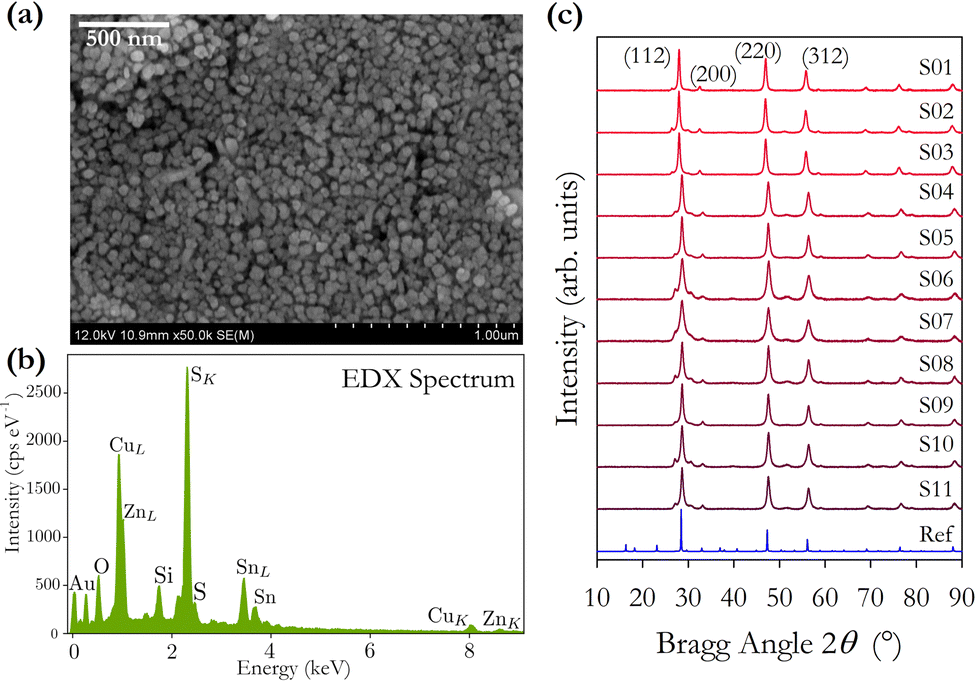 | ||
| Fig. 1 (a) SEM image of sample S01 at 50k magnification. Average particle size is 51 ± 9 nm. The domain size inferred from XRD data is 41.7 ± 1.9 nm. (b) EDX spectrum of sample S01 indicating a Cu-poor, Zn-rich composition. (c) X-ray diffraction spectra for as-synthesised nanocrystal samples S01–S11. For comparison, the reference plot for kesterite Cu2ZnSnS4 (PDF 00-026-0575) is also shown. | ||
| Sample | Lattice a (Å) | Parameters c (Å) | Domain size τ (nm) | Band gap Eg (eV) | Main Raman peak (cm−1) |
|---|---|---|---|---|---|
| S01 | 5.407 ± 0.003 | 10.869 ± 0.004 | 42 ± 2 | 1.108 ± 0.003 | 337.8 ± 0.1 |
| S02 | 5.403 ± 0.007 | 10.868 ± 0.005 | 36 ± 4 | 1.238 ± 0.002 | 336.0 ± 0.1 |
| S03 | 5.402 ± 0.007 | 10.868 ± 0.005 | 37 ± 4 | 0.856 ± 0.003 | 335.3 ± 0.1 |
| S04 | 5.397 ± 0.016 | 10.866 ± 0.007 | 28 ± 4 | 1.078 ± 0.001 | 335.4 ± 0.1 |
| S05 | 5.394 ± 0.017 | 10.866 ± 0.008 | 32 ± 6 | 1.251 ± 0.001 | 336.0 ± 0.1 |
| S06 | 5.386 ± 0.020 | 10.865 ± 0.009 | 22 ± 6 | 1.007 ± 0.002 | 336.0 ± 0.1 |
| S07 | 5.394 ± 0.017 | 10.866 ± 0.008 | 19 ± 6 | 1.257 ± 0.001 | 336.0 ± 0.1 |
| S08 | 5.390 ± 0.020 | 10.866 ± 0.009 | 28 ± 6 | 1.262 ± 0.001 | 335.3 ± 0.1 |
| S09 | 5.392 ± 0.020 | 10.866 ± 0.008 | 33 ± 4 | 1.093 ± 0.001 | 335.3 ± 0.1 |
| S10 | 5.392 ± 0.017 | 10.866 ± 0.008 | 29 ± 6 | 1.14 ± 0.03 | 328.3 ± 0.3 |
| S11 | 5.392 ± 0.018 | 10.866 ± 0.008 | 30 ± 5 | 1.23 ± 0.09 | 331.4 ± 0.3 |
| Average | 5.395 ± 0.003 | 10.867 ± 0.002 | 31 ± 7 | 1.14 ± 0.13 | 334.8 ± 2.6 |
The X-ray diffraction patterns in Fig. 1(c), and the corresponding determined lattice parameters in Table 1, confirm the expected tetragonal kesterite (I![[4 with combining macron]](https://www.rsc.org/images/entities/char_0034_0304.gif) ) crystal structure of CZTS with lattice constants a and c differing from the literature values by 0.4% and 0.04%.8 The variation in domain sizes reported in Table 1 are manifested in the observed variation in peak widths of the X-ray diffraction patterns. A weak X-ray peak at 28° just below the main (112) reflection is observed in all samples which disappears upon subsequent annealing. We have been unable to determine the origin of this weak feature.
) crystal structure of CZTS with lattice constants a and c differing from the literature values by 0.4% and 0.04%.8 The variation in domain sizes reported in Table 1 are manifested in the observed variation in peak widths of the X-ray diffraction patterns. A weak X-ray peak at 28° just below the main (112) reflection is observed in all samples which disappears upon subsequent annealing. We have been unable to determine the origin of this weak feature.
Samples S01–S04 were prepared using different rinsing and extraction chemicals as described above. We find a 0.2% increase in the average lattice constant a for samples S05–S11 compared with samples S01–S04, and a 0.02% increase in lattice constant c. We interpret this very small change as demonstrating minimal impact on the overall crystal structure when using different chemicals for rinsing, extraction, and solvents for inks. We see a more significant 22% increase in domain size with the second chemical regime indicating that the size of the extracted particles does depend on the chemicals used for rinsing, centrifuging, and preparing inks.
Although the range of lattice constants is small as expected, there is no clear correlation between the values of a and c and the energy band gap Eg.
| Sample | EDX | ICPMS | ||||||
|---|---|---|---|---|---|---|---|---|
| Cu | Zn | Sn | S | Cu | Zn | Sn | S | |
| S01 | 19.0(1.2) | 25.2(1.5) | 8.6(0.3) | 47.2(1.1) | ||||
| S02 | 23.0(1.2) | 18.5(1.3) | 12.2(0.4) | 46.3(0.4) | 23.86 | 16.42 | 12.47 | 47.26 |
| S03 | 19.7(1.7) | 25(3) | 9.6(0.4) | 46(3) | 20.78 | 21.13 | 10.12 | 47.97 |
| S04 | 24.3(1.0) | 15.9(1.2) | 12.2(0.4) | 47.6(1.0) | ||||
| S05 | 20.1(1.2) | 20.7(1.6) | 11.1(0.4) | 48.1(1.2) | ||||
| S06 | 20.1(1.0) | 19.3(1.1) | 10.9(0.3) | 49.7(0.8) | ||||
| S07 | 20.6(0.9) | 16.1(1.2) | 12.5(0.3) | 50.8(1.2) | ||||
| S08 | 17.2(0.6) | 18.9(0.7) | 10.0(0.3) | 53.9(0.7) | 20.29 | 18.68 | 9.57 | 51.47 |
| S09 | 19.0(0.4) | 17.8(0.5) | 10.6(0.2) | 52.6(0.4) | 20.69 | 18.69 | 10.17 | 50.45 |
| S10 | 20.1(0.7) | 18.0(1.1) | 11.1(0.3) | 50.8(0.7) | 21.84 | 19.92 | 10.41 | 47.84 |
| S11 | 18.5(0.8) | 20.4(1.0) | 10.2(0.3) | 51.0(0.8) | 20.72 | 20.11 | 9.83 | 49.34 |
| Average | 20(3) | 20(4) | 10.8(1.2) | 49(3) | 21.4(1.4) | 19.2(1.7) | 10.4(1.1) | 49.1(1.7) |
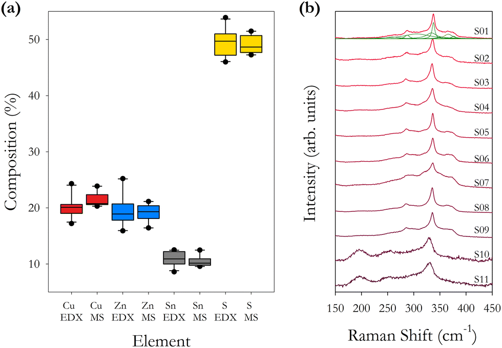 | ||
| Fig. 2 (a) Box plots of percentage element concentration for Cu, Zn, Sn and S from Table 2. Separate plots are shown for the EDX and ICPMS data for each sample. (b) Raman spectra for as-synthesised samples S01–S11 using an excitation wavelength of 785 nm. Individual fitted Raman peaks are shown for sample S01. | ||
Table 3 presents the empirical composition and cation ratios determined from EDX and ICPMS data. These data, and the average of all samples, confirm that the samples are Cu-poor and Zn-rich as expected from the initial formulation of the precursor compounds which was set at Cu/(Zn + Sn) = 0.84 and Zn/Sn = 1.25, and compares with the average values across all samples of 0.67 and 1.9. Although the precursor ratios remained constant for each sample, significant variations in the final cation ratios are observed.
| Sample | Empirical composition from EDX | Cation ratios from EDX | Cation ratios from ICPMS | ||
|---|---|---|---|---|---|
| Cu/(Zn + Sn) | Zn/Sn | Cu/(Zn + Sn) | Zn/Sn | ||
| S01 | Cu1.61Zn2.14Sn0.73S4 | 0.56(5) | 2.92(20) | ||
| S02 | Cu1.98Zn1.59Sn1.06S4 | 0.75(6) | 1.51(12) | 0.83 | 1.32 |
| S03 | Cu1.72Zn2.20Sn0.84S4 | 0.57(7) | 2.60(3) | 0.67 | 2.09 |
| S04 | Cu2.04Zn1.34Sn1.03S4 | 0.86(6) | 1.30(11) | ||
| S05 | Cu1.67Zn1.73Sn0.92S4 | 0.63(6) | 1.87(16) | ||
| S06 | Cu1.69Zn1.56Sn0.88S4 | 0.67(5) | 1.77(12) | ||
| S07 | Cu1.63Zn1.27Sn0.98S4 | 0.72(5) | 1.29(11) | ||
| S08 | Cu1.27Zn1.40Sn0.74S4 | 0.59(3) | 1.89(9) | 0.72 | 1.95 |
| S09 | Cu1.44Zn1.35Sn0.81S4 | 0.67(3) | 1.68(6) | 0.72 | 1.84 |
| S10 | Cu1.58Zn1.42Sn0.87S4 | 0.69(4) | 1.63(11) | 0.72 | 1.91 |
| S11 | Cu1.45Zn1.60Sn0.80S4 | 0.61(4) | 2.00(12) | 0.69 | 2.05 |
| Average | 0.67(10) | 1.9(6) | 0.72(6) | 1.9(3) | |
The ICPMS data show that smaller compositional fluctuations are present compared with the EDX data, with the data for Sn concentration being very stable in ICPMS as a consequence of it being the heaviest element. It is also noted that the Cu/(Zn + Sn) ratio is less variable across the different samples compared with the Zn/Sn cation ratio. This would indicate that the concentration of Zn has the largest fluctuations, as observed in Fig. 2(a). The two techniques average the elemental concentration over a determined but different volume of material. We find that using the EDX K lines for determining the concentrations of Cu, Zn and S, and using the EDX L line to determine the concentration of Sn gives the closest results when comparing EDX and ICPMS. The ICPMS technique will average the composition over a large volume of material prepared from 5–10 mg of powder, hence the more consistent ICPMS values.
Variation of films based on post-deposition annealing temperatures
Annealing of as-deposited CZTS films, usually in a S-rich environment, is an essential step in the fabrication of thin-film PV devices. To explore the impact of annealing on our samples, thin films fabricated by spin coating from nanocrystal ink batch S11 were annealed at a range of temperatures from 400–600 °C and at times from 30 to 180 minutes in a H2S:N2 (20:80) gaseous environment. Fig. 3 presents SEM images at magnifications of 1k and 10k for samples annealed for 1 hour at temperatures in the range of 400–600 °C. A visual inspection confirms that films annealed up to 500 °C appear smooth, with those annealed at 550 °C or above appearing matt.
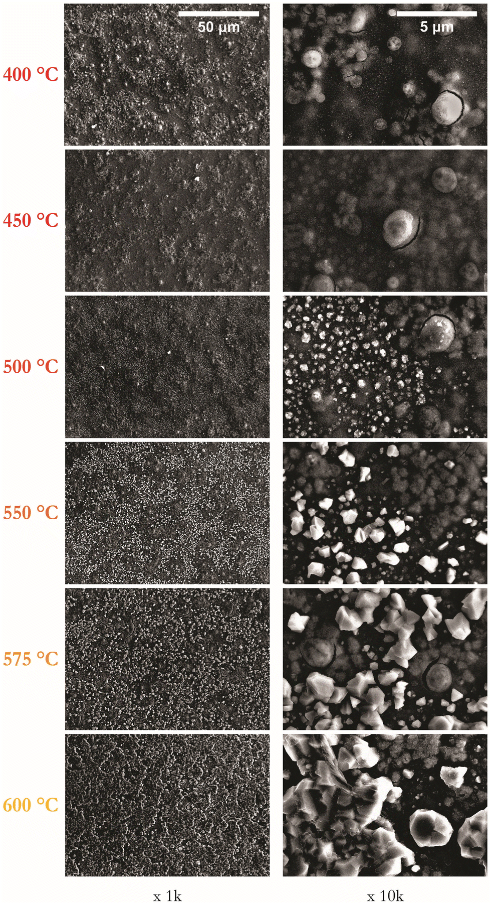 | ||
| Fig. 3 Series of representative SEM images of CZTS thin films as a function of annealing temperature from 400 to 600 °C at 1 hour shown at magnifications of 1k and 10k. | ||
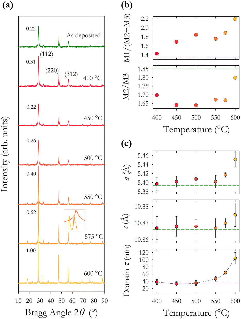 | ||
| Fig. 4 (a) XRD spectra for thin films annealed at temperatures 400–600 °C for one hour. The relative intensity of the main (112) peak is shown ranging from 0.22 to 1.00. The inset shows the peaks for the three highest temperature annealed samples plotted over the range 28–29° for the Bragg angle. The glass substrate annealed at 600 °C was distorted which may have caused a peak shift. (b) Intensity ratios of three principal Bragg peaks M1 (112), M2 (220) and M3 (312) plotted as a function of annealing temperature showing changes in the structure factor. The ratio for as-synthesised CZTS is shown as a dashed line. (c) Tetragonal lattice parameters a and c, and the average domain size τ plotted as a function of annealing temperature. Values for as-synthesised CZTS are shown as horizontal dashed lines. | ||
The intensity ratios of the main Bragg peaks M1 at 28.5° (112), M2 at 47.3° (220) and M3 at 56.2° (312) are plotted in Fig. 4(b). The main peak M1 becomes more intense with increasing annealing temperature with the ratio M1/(M2 + M3) increasing from 1.4 to 2.2. The ratio of the other peaks M2/M3 also changes with temperature, initially falling to a minimum at 500 °C and increasing to a maximum at 600 °C. These changes arise from changes in the X-ray scattering factor due to changing atoms on the kesterite lattice sites,8 possibly enhanced through the diffusion of Na from the glass substrates into the CZTS film. The film annealed at 600 °C has the (101) peak at 18.3° split into two, potentially showing the evolution of a secondary phase at higher annealing temperatures.
The lattice constants a and c and the scattering domain size τ for CZTS, determined from X-ray data, are plotted in Fig. 4(c). Up to an annealing temperature of 550 °C there is no clear change in either the lattice constants a and c or the domain size τ. The sample annealed at 600 °C showed a deformation of the glass substrate which may explain the observed increase in the lattice constants a and c at 600 °C. On a related note, solid state grown CZTS polycrystals are known to undergo a disorder phase transition at around 500 K with the transition having a width of 150 K with a correspondingly larger lattice constant.8 The observed trend in Fig. 4(c) for increasing lattice constant a may indicate increasing disorder, although the lattice constant observed here is smaller than for bulk CZTS polycrystals. The extent of any disorder in the bulk polycrystal samples will also be dependent on the cooling method. For these samples this is very slow over a 24 hour period which will likely minimise disorder. Our samples exhibit increasing lattice constant a at 575 and 600 °C. Raman spectra in Fig. 7(b) also show evidence of disordered kesterite peaks at 330 cm−1. Taken together this suggests the presence of disordered kesterite in samples annealed above 500 °C. More clearly identified in Fig. 4(c) is the increasing domain size τ, where annealing above 500 °C increases the scattering domain. This is important when considering the motivation to have large grained absorber layers in CZTS PV devices. This behaviour has also been observed in CZTSe nanoparticle films.31 Sodium is known to impact grain growth, morphology, and device performance.32 Enhanced Na diffusion from the soda lime glass substrates at higher temperatures will have an impact on these samples, and may well promote the domain growth observed in the X-ray data presented in Fig. 4.
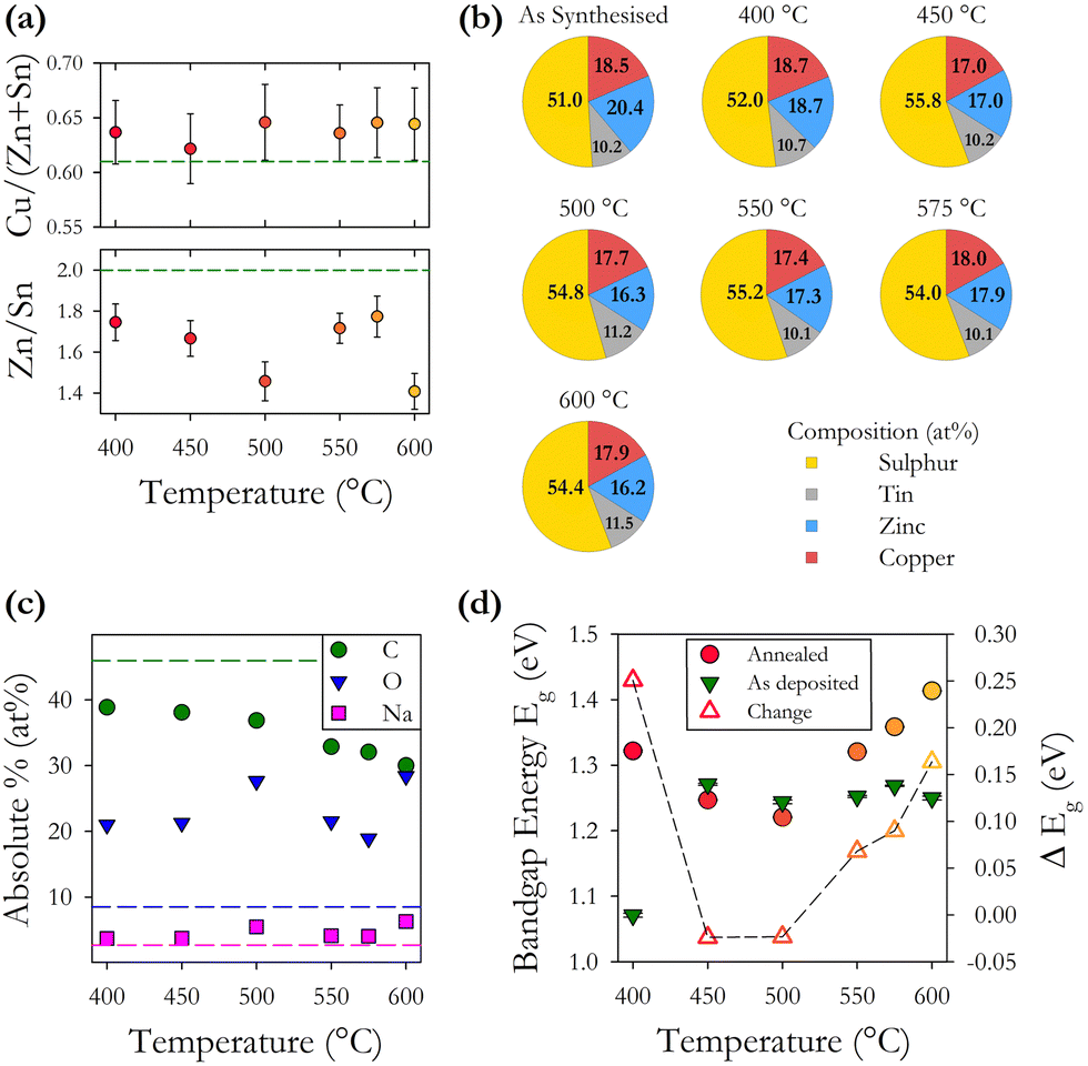 | ||
| Fig. 5 (a) Cation ratios Cu/(Zn + Sn) and Zn/Sn plotted as a function of annealing temperature. Values for as-synthesised CZTS are shown as horizontal dashed lines. (b) Normalised composition of as-synthesised CZTS particles and annealed CZTS films showing proportion of Cu, Zn, Sn and S. (c) Absolute composition (%) of as-synthesised particles and annealed films giving percentage of other main elements C, O and Na found to be present. Horizontal dashed lines indicate as synthesised composition. (d) Variation in energy band gap Eg for as-deposited films and annealed films as a function of annealing temperature. The change in Eg with annealing is shown as an open triangle Δ, the dashed line is a guide. | ||
EDX analysis was undertaken using a reduced acceleration voltage of 12 keV as numerical simulations demonstrated that the electron interaction volume was confined to the thin-film and not the substrate. Using the EDX data, we plot in Fig. 5(b) the normalised percentages of the four CZTS elements. This shows that the concentration of sulphur is increased by annealing but does not change systematically with increasing annealing temperature. The relative concentration of cations remains more or less constant except for a small decrease in the relative proportion of zinc. These findings would suggest that our gaseous atmosphere of H2S:N2 (20:80) has a suitable amount of sulphur to achieve complete annealing, other studies have suggested that a less sulphur-rich environment is favourable.33,34 Our analysis of the observed variation between 11 samples fabricated under the same conditions, presented above, indicates a range of standard deviations in the elemental concentration. The change observed in the relative elemental concentration with annealing is very similar to the initial standard deviation. From this, we can infer that annealing under the conditions described here does not significantly alter the relative elemental concentration as shown in Fig. 5(a) and (b).
We also find through EDX analysis the presence of carbon, oxygen, and sodium in our films, as shown in Fig. 5(c). Carbon is present at the highest level and is known to be a residue of the organic solvents used during nanoparticle synthesis. Increasing annealing temperature reduces the proportion of carbon through temperature induced decomposition of the residual organic compounds resulting in a 10–15% decrease in the percentage of carbon across the annealing range. Annealing is observed to incorporate oxygen into our films with a typical increase of 12% in the oxygen content. The main source of oxygen is the acetylacetonate precursors during synthesis, and the expected incorporation of oxygen during the 30 second soft bake at 300 °C to remove the residual solvent during spin coating. Sodium is known to diffuse into the films from the glass substrates during annealing, however, here we observe only a small increase of between 1 and 3% in the proportion of sodium after annealing, with no clear trend as a function of temperature. A small amount of sodium, 2.7%, is present in the as-synthesised nanoparticles, possibly from the precursor reactants. EDX mapping reveals a non-uniform distribution of sodium and oxygen in the films.
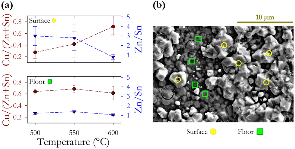 | ||
| Fig. 6 (a) Variation in cation ratios for surface and floor regions of annealed films as a function of annealing temperature. (b) SEM image identifying distinct surface and floor regions. | ||
Variation of films with post-deposition annealing – time
To explore the impact of annealing time on the physical and structural properties of CZTS thin films, a series of samples were annealed in the H2S:N2 (20:80) environment at 500 °C for times ranging from 30 to 180 minutes. Thin films for annealing were all prepared from CZTS nanocrystal ink batch S10.
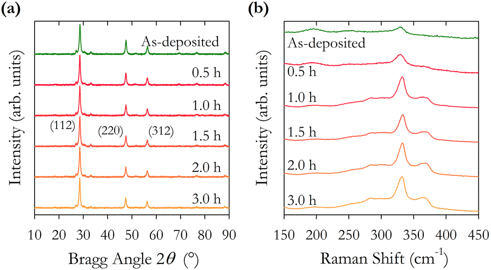 | ||
| Fig. 7 (a) XRD spectra for thin films annealed at 500 °C as a function of annealing time. (b) Raman spectra for as-synthesised CZTS particles and films annealed at 500 °C for different durations using an excitation wavelength of 785 nm. | ||
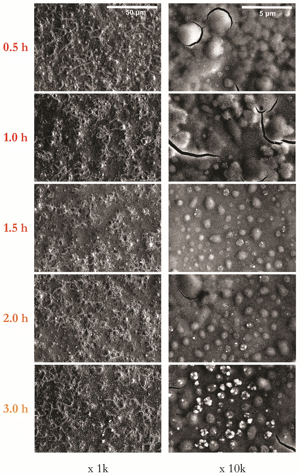 | ||
| Fig. 8 Series of representative SEM images as a function of annealing at 500 °C with time from 0.5–3.0 hours shown at magnifications of 1k and 10k. | ||
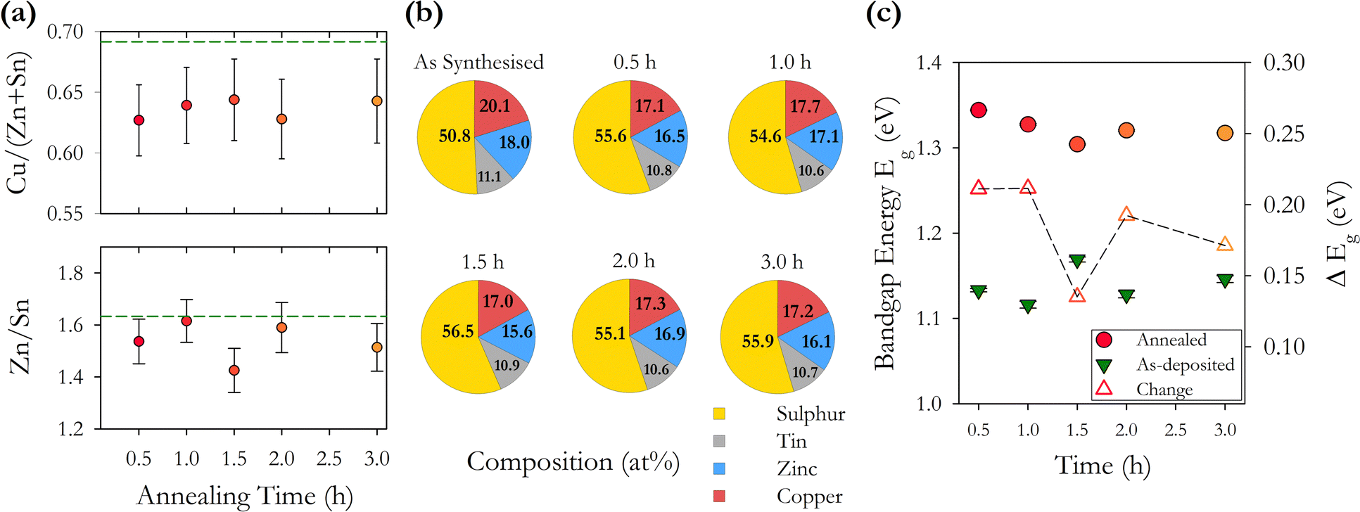 | ||
| Fig. 9 (a) Cation ratios Cu/(Zn + Sn) and Zn/Sn as a function of annealing time at 500 °C. The horizontal line shows the as-synthesised CZTS particles. (b) Normalised composition of as-synthesised CZTS particles and CZTS films annealed at 500 °C for varying times. (c) Variation in energy band gap Eg for as-deposited films and annealed films as a function of annealing time at 500 °C. The change in Eg with annealing is shown as an open triangle Δ, the dashed line is a guide. | ||
CZTS compositional pie charts in Fig. 9(b) show a consistently higher concentration of sulphur after annealing with a 10% increase and no clear trend with annealing time. This is consistent with the series of samples with varying annealing temperatures. We also see a reduction in the % of Cu and Zn with the Sn % remaining more or less constant. This is also consistent with the temperature annealed series and again does not show the widely reported loss of Sn. We note that there is an increase in the energy bandgap with annealing which may be related to the increase in sulphur. There also appears to be a trend of decreasing band gap with increasing time, with the exception of the 1.5 h sample. This may be related to changes in the concentration of point defects and defect complexes with increasing annealing time.
We find that systematically changing the annealing time from 0.5–3.0 hours with a constant annealing temperature of 500 °C has less impact on the structural and optoelectronic properties of the resulting films compared with annealing at varying temperatures of 400–600 °C for 1 hour. The most significant changes happen in the first 0.5 hour of annealing with the increase of the bandgap to 1.3 eV established after a 1 hour anneal. This is as expected for changes that are thermally activated. Device fabrication protocols should be based on annealing times of no more than 1 hour to limit the energy expended in fabrication.
Conclusions
This project was conceptualised to investigate the reproducibility of CZTS hot injection synthesis of nanoparticle inks and thin-film samples prepared by spin coating of inks with subsequent annealing under a sulphur rich atmosphere. We find that the collection of nanoparticles using ethanol, hexane, and isopropanol with a subsequent ink solution in hexanethiol resulted in a higher concentration by weight although there was no observed change in the chemical composition of particles. We observe a 22% increase in the domain size using ethanol, hexane and isopropanol compared with the original toluene-isopropanol regime first used by Guo et al.10 Hot injection synthesis at 225 °C produced nanoparticle films with an average diameter of 51 ± 9 nm and an average scattering domain size of 41.7 ± 1.9 nm indicating that many particles will be composed of a single domain. Comparison of compositions determined via EDX and ICPMS demonstrates the need for careful selection of EDX lines to obtain reliable findings. We identify the CuK, ZnK, SnL, and SK lines as optimum. X-ray diffraction confirms the expected kesterite lattice structure with the a and c lattice constants differing from the literature values by 0.4% and 0.04% respectively. We find the lowest variation in Sn (measured by ICPMS) at ±1.2%, and the largest for S (measured by EDX) at ±3.8%. ICPMS shows the lowest compositional fluctuations compared with EDX. Zn has the largest fluctuations. Resonant Raman measurements show the expected peaks associated with disordered CZTS, and a weak feature related to SnS, but overall little evidence of secondary phases. As-synthesised inks have an average energy band gap of 1.14 eV.Annealing in a sulphur rich atmosphere in a range of temperatures from 400 to 600 °C has minimal impact on the Cu/(Zn + Sn) cation ratios, with a decrease of −0.4 in the Zn/Sn ratio. The concentration of S does increase with annealing but not systematically with increasing annealing temperature. Annealing does not significantly alter the relative elemental concentration. At higher annealing temperatures 500–600 °C the bandgap shows a linear increase in energy, increasing by +0.15 eV at 600 °C. Abnormal CZTS grains form above 500 °C where the Zn/Sn ratio decreases from 3 to 1 going from 500 to 600 °C, while the Cu/(Zn + Sn) ratio increases from 0.28 to 0.72. The standard deviation of the elemental concentrations is much larger for abnormal grains with the change of cation ratios indicating the loss of Zn. At the highest annealing temperature (600 °C) the composition of the abnormal grains approaches that of the underlying floor layer as a result of enhanced elemental diffusion. A significant increase in scattering domain size τ is observed at the highest annealing temperature increasing from 38 to 104 nm. We conclude that device fabrication protocols should have an annealing time of no more than 1 hour.
Author contributions
Project conceptualisation, data collection and analysis were carried out by KS. DH and MS supervised the project. The original draft of the manuscript was prepared by DH with additional review and editing by KS and MS.Conflicts of interest
There are no conflicts to declare.Acknowledgements
The authors thank Dr. Chris Otley for ICPMS measurements.References
- A. Polman, M. Knight, E. C. Garnett, B. Ehrler and W. C. Sinke, Science, 2016, 352, aad4424, DOI:10.1126/science.aad4424.
- C. Yan, J. L. Huang, K. W. Sun, S. Johnston, Y. F. Zhang, H. Sun, A. B. Pu, M. R. He, F. Y. Liu, K. Eder, L. M. Yang, J. M. Cairney, N. J. Ekins-Daukes, Z. Hameiri, J. A. Stride, S. Y. Chen, M. A. Green and X. J. Hao, Nat. Energy, 2018, 3, 764–772, DOI:10.1038/s41560-018-0206-0.
- S. N. Hood, A. Walsh, C. Persson, K. Iordanidou, D. Huang, M. Kumar, Z. Jehl, M. Courel, J. Lauwaert and S. Lee, J. Phys.: Energy, 2019, 1, 042004, DOI:10.1088/2515-7655/ab2dda.
- S. Y. Chen, A. Walsh, X. G. Gong and S. H. Wei, Adv. Mater., 2013, 25, 1522–1539, DOI:10.1002/adma.201203146.
- S. Y. Chen, J. H. Yang, X. G. Gong, A. Walsh and S. H. Wei, Phys. Rev. B: Condens. Matter Mater. Phys., 2010, 81, 245204, DOI:10.1103/PhysRevB.81.245204.
- O. Gunawan, T. Gokmen and D. B. Mitzi, J. Appl. Phys., 2014, 116, 084504, DOI:10.1063/1.4893315.
- J. J. S. Scragg, J. K. Larsen, M. Kumar, C. Persson, J. Sendler, S. Siebentritt and C. P. Bjorkman, Phys. Status Solidi B, 2016, 253, 247–254, DOI:10.1002/pssb.201552530.
- C. J. Bosson, M. T. Birch, D. P. Halliday, K. S. Knight, A. S. Gibbs and P. D. Hatton, J. Mater. Chem. A, 2017, 5, 16672–16680, 10.1039/c7ta03603e.
- C. J. Bosson, M. T. Birch, D. P. Halliday, C. C. Tang, A. K. Kleppe and P. D. Hatton, Chem. Mater., 2017, 29, 9829–9839, DOI:10.1021/acs.chemmater.7b04010.
- Q. J. Guo, H. W. Hillhouse and R. Agrawal, J. Am. Chem. Soc., 2009, 131, 11672–11673, DOI:10.1021/ja904981r.
- H. Wei, W. Guo, Y. J. Sun, Z. Yang and Y. F. Zhang, Mater. Lett., 2010, 64, 1424–1426, DOI:10.1016/j.matlet.2010.03.034.
- S. Siebentritt, Sol. Energy Mater. Sol. Cells, 2011, 95, 1471–1476, DOI:10.1016/j.solmat.2010.12.014.
- S. Siebentritt, Thin Solid Films, 2013, 535, 1–4, DOI:10.1016/j.tsf.2012.12.089.
- K. P. Stroh, MSc thesis, University of Durham, 2019, https://etheses.dur.ac.uk/13022/ Search PubMed.
- Q. Guo, G. M. Ford, W. C. Yang, B. C. Walker, E. A. Stach, H. W. Hillhouse and R. Agrawal, J. Am. Chem. Soc., 2010, 132, 17384–17386, DOI:10.1021/ja108427b.
- S. Y. Chen, X. G. Gong, A. Walsh and S. H. Wei, Appl. Phys. Lett., 2010, 96, 021902, DOI:10.1063/1.3275796.
- Y. Altowairqi, A. Alsubaie, K. P. Stroh, I. G. Perez-Marin, L. Bowen, M. Szablewski and D. P. Halliday, Mater. Today: Proc., 2019, 18, 473–486, DOI:10.1016/j.matpr.2019.06.234.
- S. G. Kwon and T. Hyeon, Small, 2011, 7, 2685–2702, DOI:10.1002/smll.201002022.
- A. Khare, A. W. Wills, L. M. Ammerman, D. J. Norris and E. S. Aydil, Chem. Commun., 2011, 47, 11721–11723, 10.1039/c1cc14687d.
- D. Mora-Herrera and M. Pal, Appl. Phys. A: Mater. Sci. Process., 2022, 128, 1008, DOI:10.1007/s00339-022-06137-0.
- N. J. Carter, W. C. Yang, C. K. Miskin, C. J. Hages, E. A. Stach and R. Agrawal, Sol. Energy Mater. Sol. Cells, 2014, 123, 189–196, DOI:10.1016/j.solmat.2014.01.016.
- B. Long, S. Y. Cheng, Y. F. Lai, H. F. Zhou, J. L. Yu and Q. Zheng, Thin Solid Films, 2014, 573, 117–121, DOI:10.1016/j.tsf.2014.11.008.
- A. Khare, B. Himmetoglu, M. Johnson, D. J. Norris, M. Cococcioni and E. S. Aydil, J. Appl. Phys., 2012, 111, 083707, DOI:10.1063/1.4704191.
- J. R. Brent, D. J. Lewis, T. Lorenz, E. A. Lewis, N. Savjani, S. J. Haigh, G. Seifert, B. Derby and P. O'Brien, J. Am. Chem. Soc., 2015, 137, 12689–12696, DOI:10.1021/jacs.5b08236.
- S. Siebentritt, G. Rey, A. Finger, D. Regesch, J. Sendler, T. P. Weiss and T. Bertram, Sol. Energy Mater. Sol. Cells, 2016, 158, 126–129, DOI:10.1016/j.solmat.2015.10.017.
- C. Persson, J. Appl. Phys., 2010, 107, 053710, DOI:10.1063/1.3318468.
- M. Lang, T. Renz, A. Opolka, C. Zimmermann, C. Krammer, M. Neuwirth, H. Kalt and M. Hetterich, Appl. Phys. Lett., 2018, 113, 033901, DOI:10.1063/1.5036622.
- G. Rey, A. Redinger, J. S. Ler, T. P. Weiss, M. Thevenin, M. Guennou, B. El Adib and S. Siebentritt, Appl. Phys. Lett., 2014, 105, 112106, DOI:10.1063/1.4896315.
- B. D. Chernomordik, A. E. Beland, D. D. Deng, L. F. Francis and E. S. Aydil, Chem. Mater., 2014, 26, 3191–3201, DOI:10.1021/cm500791a.
- B. A. Williams, M. A. Smeaton, N. D. Trejo, L. F. Francis and E. S. Aydil, Chem. Mater., 2017, 29, 1676–1683, DOI:10.1021/acs.chemmater.6b05058.
- K. Sugimoto, N. Suyama, K. Nakada and A. Yamada, Jpn. J. Appl. Phys., 2017, 56, 035502, DOI:10.7567/JJAP.56.035502.
- C. Andres, T. Schwarz, S. G. Haass, T. P. Weiss, R. Carron, R. Caballero, R. Figi, C. Schreiner, M. Burki, A. N. Tiwari and Y. E. Romanyuk, Sol. Energy, 2018, 175, 94–100, DOI:10.1016/j.solener.2018.03.067.
- K. Maeda, K. Tanaka, Y. Fukui and H. Uchiki, Sol. Energy Mater. Sol. Cells, 2011, 95, 2855–2860, DOI:10.1016/j.solmat.2011.05.050.
- K. Maeda, K. Tanaka, Y. Nakano, Y. Fukui and H. Uchiki, Jpn. J. Appl. Phys., 2011, 50, 05FB09, DOI:10.1143/JJAP.50.05FB09.
Footnote |
| † Present address: Faculty of Physics, Georg-August-Universität Göttingen, Friedrich-Hund-Platz 1, 37077 Göttingen, Germany. |
| This journal is © The Royal Society of Chemistry 2024 |