
Elucidating the effect of Ag interlayer formation on the intrinsic mechanical properties of free-standing ITO/Ag/ITO thin films†
Seung Jin
Oh
 a,
Sangmin
Lee
a,
Kyung Cheol
Choi
b,
Jeong Hyun
Kwon
*c and
Taek-Soo
Kim
*a
a,
Sangmin
Lee
a,
Kyung Cheol
Choi
b,
Jeong Hyun
Kwon
*c and
Taek-Soo
Kim
*a
aDepartment of Mechanical Engineering, Korea Advanced Institute of Science and Technology (KAIST), Daejeon 34141, Republic of Korea. E-mail: tskim1@kaist.ac.kr
bSchool of Electrical Engineering, Korea Advanced Institute of Science and Technology (KAIST), Daejeon 34141, Republic of Korea
cDepartment of Display and Semiconductor Engineering, SunMoon University, Asan 31460, Republic of Korea. E-mail: love6539@sunmoon.ac.kr
First published on 1st May 2023
Abstract
The lack of characterization of the mechanical behavior of brittle indium tin oxide (ITO)-based electrodes has been a core issue for the development of advanced transparent and flexible electronics. In this study, we report the intrinsic mechanical properties of ITO/Ag/ITO (IAI) thin films measured by a free-standing tensile testing method for robust transparent electrodes. To understand the effect of Ag interlayer formation on the mechanical properties, Ag thickness is controlled (8–50 nm) by considering the stage of the film formation. Based on the tensile test, IAI thin films with a film-likely formed Ag interlayer (12–14 nm) exhibited outstanding mechanical robustness compared with island-(8 nm) or film-type (>25 nm) Ag interlayers. Notably, the most superior elongation and tensile strength (0.57 ± 0.08% and 514.3 ± 71.5 MPa) are demonstrated for 14 nm-thick Ag interlayer, which is two-fold higher than pristine ITO thin films (0.27% and 264.6 MPa). The study provides intrinsic mechanical property values and fundamental insights into the fracture mechanisms that govern the mechanical behavior of oxide/metal/oxide multilayer thin films, which is valuable for the development of flexible electronics.
Introduction
Based on their favorable electrical (<10−4 Ω cm), optical (>90%), and chemical stability properties, indium tin oxide (ITO) thin films have been used as transparent electrodes for electronic devices.1–5 However, the relatively high sheet resistance and brittleness of ITO thin films are critical drawbacks for their application in advanced flexible electronics.6–8 Recently, oxide/metal/oxide thin films have been extensively studied as alternative transparent electrodes owing to their outstanding performance, such as low sheet resistance, enhanced flexibility, and roll-to-roll process compatibility. In particular, ITO/Ag/ITO (IAI) multilayered films have attracted significant attention in the fields of flexible organic light-emitting diodes (OLEDs), flexible organic solar cells, thin-film transistors (TFTs), touch screens, semiconductors, and aeronautical engineering.9–14 Besides, a low-temperature process of IAI thin films is critically required for optoelectronic applications, which is achievable using sputtering and evaporation methods.15,16 The IAI multilayered structure satisfies all the requirements for electronics with a reduced amount of ITO thin films combined with tens of nanometer-thick Ag interlayers, whereas the typical thickness of the ITO thin films ranges between 150 and 250 nm.17,18Several studies have focused on optimizing the electrical and optical properties of ITO/Ag/ITO thin films. Jeong et al. reported that a Ag thickness of 16 nm exhibited the best transparency (86.5%) versus conductivity (4.4 Ω sq−1) with a figure of merit of 49.4 × 10⁻³ Ω−1.19 Recently, Wang et al. revealed that ∼10 nm of Ag incorporation showed the optimal combination of electrical (6.1 Ω sq−1) and optical properties (90.8%) with a higher figure of merit of 62.3 × 10⁻³ Ω−1.8 However, the tendency of catastrophic fracture of the brittle IAI thin films remains the cause of the sudden failure of devices. Studies on the intrinsic mechanical behaviors of IAI thin films have rarely been reported because direct tensile testing is restricted owing to the challenges in handling nano-thick and brittle IAI thin films. Therefore, previous studies have been limited to comparing the bending stability of ITO and IAI multilayered thin films on plastic substrates, which was demonstrated to be affected by residual stress.16,20–22 Additionally, to the best of our knowledge, the effect of the Ag interlayer on the mechanical properties of IAI thin films has not been elucidated thus far. Therefore, exploring their intrinsic mechanical properties and fracture mechanism is essential for expanding the applications of transparent conductive electrodes (TCEs).
In this study, we report the tensile and fracture behaviors of low-temperature-processed IAI multilayer thin films, as a function of the thickness of the Ag interlayer. The IAI thin films with Ag thicknesses of 8, 10, 11, 12, 13, 14, 25, and 50 nm are prepared. Each IAI structure is tested in the free-standing state to confirm whether the regulation of the Ag interlayer thickness can improve the mechanical stability and simultaneously enhance the optical and electrical properties of the thin films. Previous literature reported the aging effect of the IAI thin films when the film is exposed to oxygen, air, and light illumination.23–25 To exclude the aging effect, whole samples were stored in a vacuum desiccator (approximately −0.1 mPa, 0% relative humidity) and the test was performed within 2 weeks after the deposition. Therefore, this study aims to provide a foundation for a better understanding of the mechanical behavior of oxide/metal/oxide multilayers and new opportunities for the design of flexible electronics and mechanical nanocomposites.
Results and discussion
Preparation of free-standing IAI thin films
The preparation of a free-standing IAI thin film for tensile testing is shown in Fig. 1. As shown in Fig. 1a, the IAI thin film was deposited onto a Cu/SiO2/Si square wafer (35 × 35 mm). For ITO deposition, the thicknesses of the bottom and top ITO thin films were symmetrically defined as 45 nm to achieve effective antireflection effects, which exhibited the highest red/green/blue (RGB) average transmittance based on an optical simulation (Fig. S1, ESI†).19,26,27 To determine the effect of the Ag interlayer formation on the mechanical properties of the IAI thin films, the Ag thicknesses were varied as 8, 10, 11, 12, 13, 14, 25, and 50 nm. The IAI thin films are denoted as IAI(8), IAI(10), IAI(11), IAI(12), IAI(13), IAI(14), IAI(25), and IAI(50), respectively. The XPS depth profiles show that the IAI thin films were successfully fabricated as intended with symmetric ITO thin films at the top and bottom of the structure (Fig. S2, ESI†). A stable Ag interlayer was formed between the well-defined symmetrical ITO thin films with a proper stoichiometric composition without any detectable interfacial reaction or diffusion. Additionally, the as-deposited ITO thin films were amorphous, and the Ag interlayer was polycrystalline and dominantly oriented in the (111) direction (Fig. S3, ESI†).28,29 After the deposition of the IAI thin film, the as-deposited IAI/Cu layers were patterned into a dog-bone shape using a femtosecond laser, and subsequently free-standing tensile tests were performed (Fig. 1c).30,31 To obtain a free-standing IAI thin film, the IAI/Cu film was peeled off from the SiO2/Si substrate with the assistance of the surface tension of water (Fig. 1d). A slight force was addressed using a commercial tape to initiate and propagate the delamination between the Cu/SiO2 interface (Fig. S4, ESI†). The overall transfer process took less than 1 minute. Owing to the weak interfacial adhesion energy of Cu/SiO2 in water, the IAI/Cu film was carefully transferred onto the water surface without any damage.32 Subsequently, the sacrificial Cu layer was etched with a 0.035 M ammonium persulfate solution (Fig. 1e). Finally, the free-standing IAI thin film was obtained by substituting the Cu etchant with deionized water to prevent any possible chemical damage to the IAI thin film (Fig. 1f).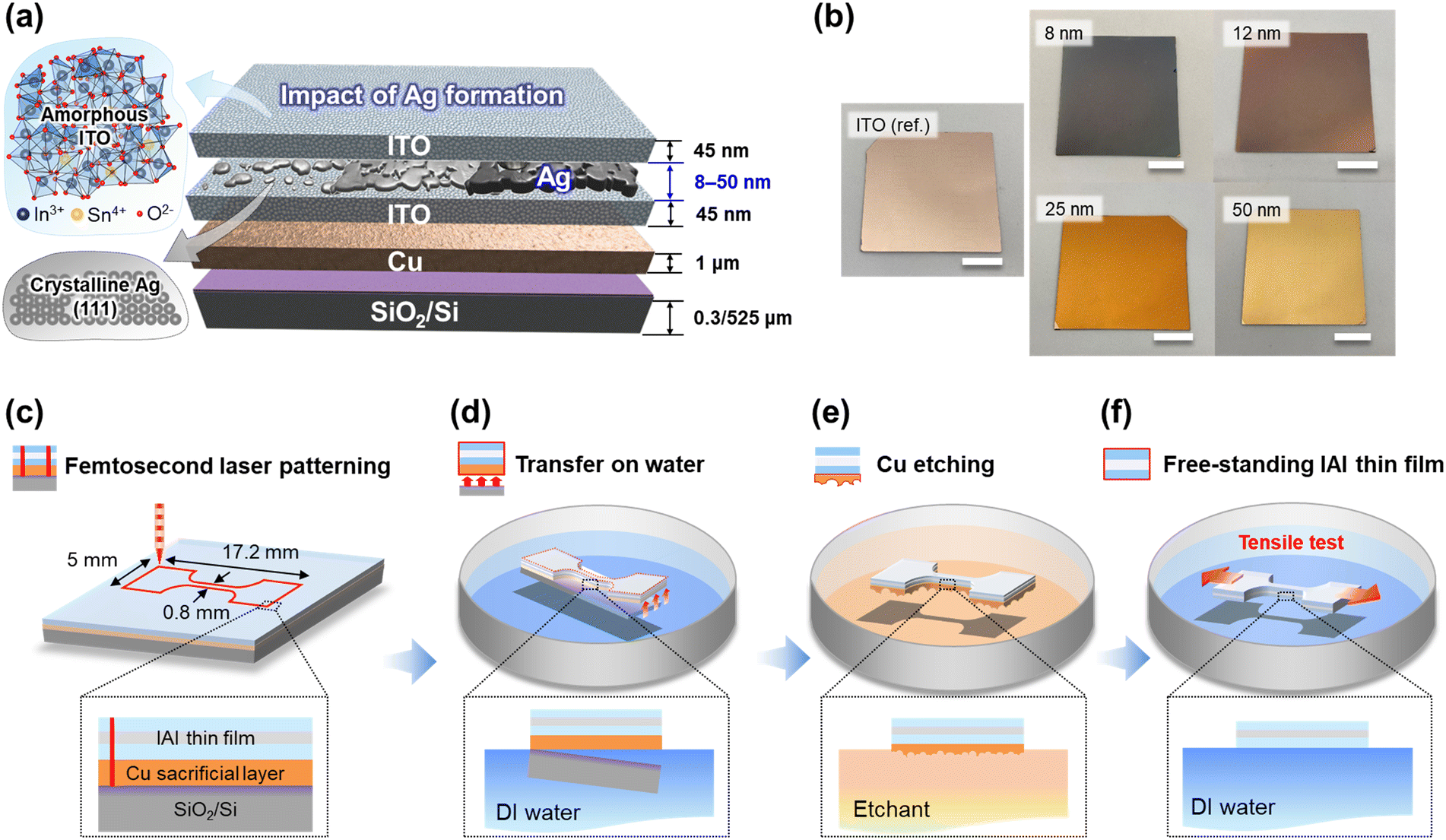 | ||
| Fig. 1 Schematics for the preparation of free-standing IAI thin films. (a) Deposition of Cu (1 μm), ITO (45 nm), Ag (8–50 nm), and ITO (45 nm) thin films on a SiO2/Si wafer. (b) Photos of the fabricated ITO and IAI thin films as a function of Ag thickness (scale bar = 10 mm). (c) Femtosecond laser patterning of the IAI/Cu layer to fabricate the dog-bone-shaped specimen. (d) Transfer of the IAI/Cu layer onto the water surface. (e) Etching of the sacrificial Cu layer. (f) Prepared free-standing IAI thin films for the tensile test. | ||
Effect of Ag interlayer thickness on mechanical properties
Photographs of the tensile test procedure are shown in Fig. 2a. By utilizing the high surface tension of water, free-standing IAI thin films are successfully tested without disrupting deformations, such as wrinkles and deflection. Additionally, the effect of residual stress was excluded because the IAI thin films on the water surface could freely release the substrate constraint.33 Moreover, the effect of surface roughness was negligible because there was no significant difference in root mean square roughness (Rq) with respect to the Ag interlayer thickness (Fig. S5, ESI†). Gripping of the free-standing and dog-bone-shaped IAI thin films was accomplished by van der Waals adhesion between the polydimethylsiloxane (PDMS) and IAI thin films. After gripping, a tensile test was conducted by horizontal loading using a high-resolution linear actuator at a strain rate of approximately 5.8 × 10⁻⁵ s−1 (Fig. 2b and Fig. S6, ESI†). During the tensile test, the digital image correlation (DIC) method was used to precisely measure the applied strain by tracking the designated patterns using a charge-coupled device (CCD) camera.34,35 At the last moment of the tensile test, the fracture of the IAI thin films occurred catastrophically according to the crack branching phenomenon (that is, multiple shear bands), which represents the typical failure of brittle materials.31,36 This tendency of brittle cracking of the IAI thin films may result in a sudden increase in their electrical resistivity, thereby causing unexpected failure of the devices. The characteristics of completely brittle failure were also observed in the stress–strain curves of the IAI thin films, as a function of the Ag thickness (Fig. 2c). Independent of the Ag interlayer thickness, the curves exhibited a linear increase in the applied stress according to the applied strain, and plastic deformation was not detected. Therefore, considering the precise intrinsic elongation, it is essential to conservatively prevent the breakage of brittle IAI thin films for the design of flexible electronics.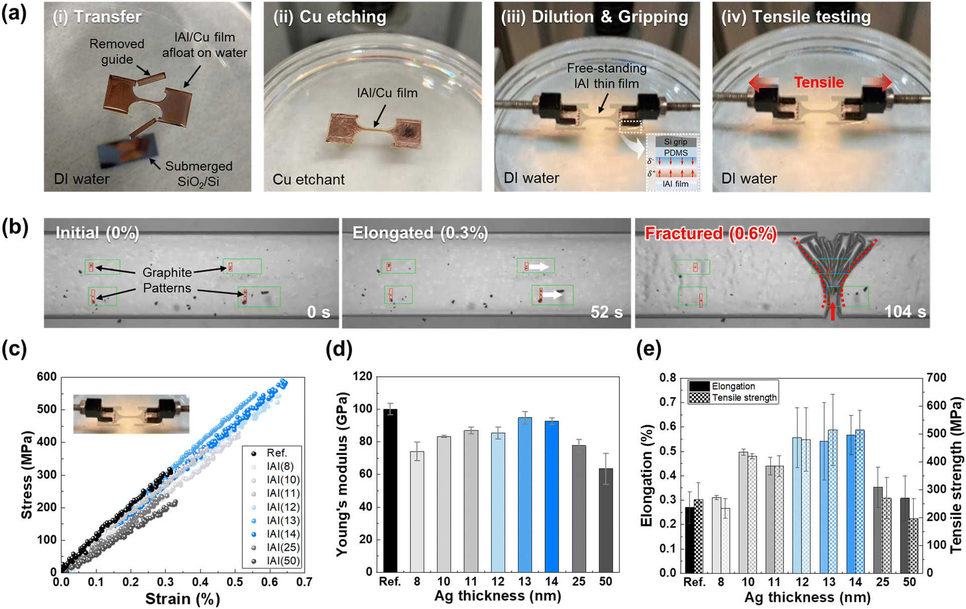 | ||
| Fig. 2 Tensile testing of free-standing IAI thin films. (a) Photos of the tensile testing procedure for IAI thin films. (b) CCD camera images during the tensile loading. (c) Representative stress–strain curves of the ITO (Reference) and IAI thin films as a function of Ag thickness. (d) Intrinsic Young's modulus of the IAI thin films. (e) Intrinsic elongation and tensile strength of the IAI thin films. | ||
To date, the intrinsic Young's modulus and elongation of IAI thin films have not yet been reported. Based on the stress–strain curves, Table S1 (ESI†) lists the intrinsic Young's modulus, elongation, and resultant tensile strength of the IAI thin films depending on the Ag thickness. As shown in Fig. 2d, the Young's modulus of the IAI thin films with Ag thicknesses ranging from 8 to 13 nm increased from 74 ± 6 GPa to 95 ± 4 GPa and decreased for 14, 25, and 50 nm to 93 ± 2 GPa, 78 ± 4 GPa, and 63 ± 10 GPa, respectively. Compared with the 90 nm-thick reference ITO thin film, the Young's modulus values of the fabricated IAI films were relatively low because of the premature formation of the Ag interlayer and its lower Young's modulus (<60 GPa)37 than that of the ITO thin films (103.2 GPa). Interestingly, the intrinsic Young's moduli of IAI thin films did not obey the rule of mixture, which support that our reporting values are worthy for the accurate mechanical analysis of flexible electronics (Fig. S7, ESI†). Additionally, the rule of mixture results indicates that the films’ compactness maximized for the IAI(13) and IAI(14) thin films. As shown in Fig. 2e, the elongation of the IAI thin films with Ag thicknesses ranging from 8 to 14 nm increased from 0.31 ± 0.01% to 0.57 ± 0.08%, and decreased for 25 and 50 nm to 0.35 ± 0.08% and 0.31 ± 0.09%, respectively. The highest elongation was recorded for IAI(14) thin films (0.57 ± 0.08%). Thus, the elongation of the fabricated IAI thin films was superior, independent of the Ag thickness, compared with that of the reference ITO thin film (0.27 ± 0.06%). The tensile strength of the IAI thin films showed a similar trend to the elongation as a function of Ag thickness. These results suggest that IAI thin films with an optimized Ag thickness of 12–14 nm, as an alternative to conventional ITO thin films, can significantly improve the mechanical stretchability of flexible electronics. Additionally, the measured intrinsic mechanical properties enable the transition from IAI multilayer modeling to equivalent single-layer modeling for accurate finite element analysis (FEA) modeling to describe the mechanical behavior of IAI thin films.38,39
To gain a better insight into the role of the Ag interlayer on the mechanical properties, structural characterization of the Ag/ITO (AI) and IAI thin films was conducted using SEM. Fig. 3a shows the surface morphologies of the AI thin films for the as-deposited Ag interlayer and the layer after exposure to the argon/oxygen (Ar/O2) plasma atmosphere, as a function of the Ag thickness. For the as-deposited Ag layer, the film formation followed the multistep processes of metal growth on oxides: (1) the nucleation of discrete nano-sized clusters (islands), followed by coalescence into large and irregular clusters, (2) the formation of a premature film-like network at a specific percolation threshold, and (3) the transition to a continuous film with increasing metal thickness.40 To understand the Ag film formation, a thermodynamic criterion can be introduced, and the growth mode of Ag is determined by the following energy difference (eqn (1)):
| Δγ = −γs + γi + γf | (1) |
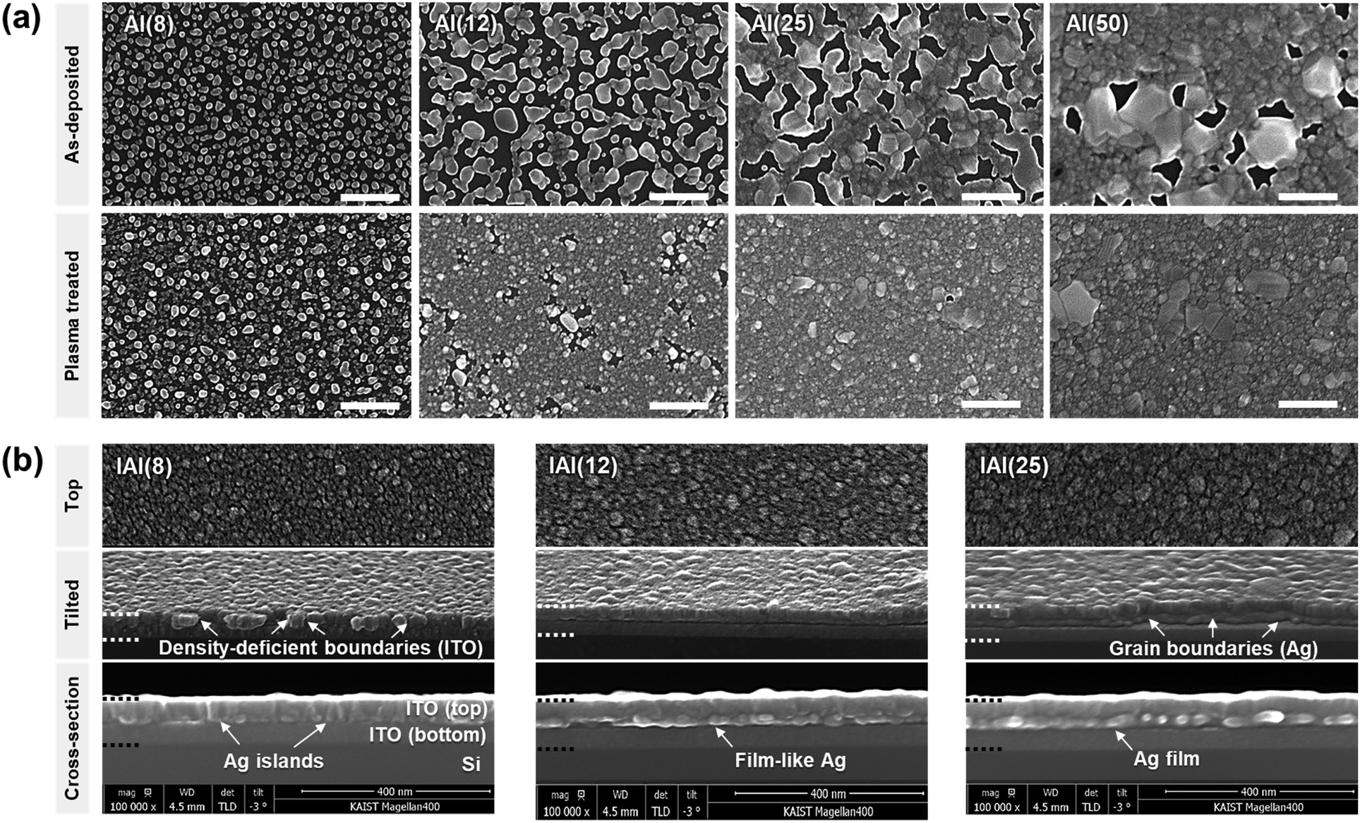 | ||
| Fig. 3 SEM images of the surface morphologies of Ag interlayer and fractured surfaces of the IAI thin films as a function of Ag thickness. (a) Surface morphologies of the as-deposited and plasma-treated Ag layer on the bottom ITO surface. Plasma-treated images showing the effect of Ar/O2 plasma during the top ITO deposition (scale bar = 500 nm). (b) Top, tilted, and cross-sectional images of the fractured surface of IAI thin films. Defective regions in the top ITO and Ag interlayer are exposed at the tilted images. | ||
where Δγ is the energy difference between the substrate (ITO) and film (Ag), γs is the surface free energy of the substrate, γf is the free energy of the film, and γi is that of the interface between the substrate and film. Generally, in the case of metal films, the clusters are more bound to each other than to the substrates (that is, Δγ > 0). Therefore, the Volmer–Weber (island) growth mode is observed for the Ag thin films.41–44 For the images of plasma-treated Ag interlayer, the diffusion of Ag was confirmed after exposure to the ITO sputtering atmosphere without direct collision of ITO clusters. Therefore, the change in the Ag morphology originates from the Ar/O2 plasma, which enhances the wetting property of the exposed bottom ITO surface. The Ar/O2 plasma in the partial O2 environment increases the surface energy of the ITO surface, thereby contributing to the formation of a film-like state.45,46 With a decrease in γi, the Ag atoms interact more strongly with the ITO substrate than with each other. Additionally, the local thermal energy that occurred during the sputtering of the top ITO thin films may have induced additional diffusion and percolation of the Ag clusters. The low-temperature diffusion of the island-type Ag interlayer is accelerated by the small size of Ag nuclei.47,48 Based on our observations of the AI films, we can conclude that IAI(8) contains isolated Ag islands, IAI(12–14) contains a film-like Ag interlayer, and IAI(25–50) contains a continuous Ag film interlayer.
It is widely known that structural defects, such as voids, density-deficient boundaries, and pinholes, can significantly impact the fracture behavior of amorphous oxide thin films.49–51Fig. 3b represents the structural characteristics of the IAI thin films as a function of the Ag interlayer thickness. For the IAI(8) thin film, the Ag islands functioned as a point nucleation site for the top ITO, thereby the top ITO formed a distinct columnar microstructure. Our previous observation using high-angle annular dark field-scanning transmission electron microscope (HAADF-STEM) found that the boundaries of ITO particles are significantly density-deficient.31 Therefore, the IAI(8) thin films exhibiting poor mechanical properties due to the island Ag interlayer itself and the defective top ITO boundaries.50 For the case of IAI(10–14), the film-like Ag interlayer contributed to the formation of a denser top ITO by functioning as a plane nucleation site. Therefore, the critical defects, which are density-deficient boundaries of the columnar ITO structure, were reduced. Thus, in combination with the densified Ag interlayer and top ITO, the Young's modulus, elongation, and tensile strength were significantly increased. For the IAI(25) and IAI(50) thin films, Young's modulus decreased owing to the increased portion of the Ag film layer. Additionally, elongation was also deteriorated owing to the extended and intensified grain boundaries around the crystallites as the crystallization of the Ag interlayer progressed (Fig. S3, ESI†). Therefore, film-like formation of the Ag interlayer is very important to enhance the mechanical properties of oxide/metal/oxide thin films.
Through the cross-sectional SEM observation, it was difficult to confirm the actual in-plane morphology of the Ag interlayer of IAI thin films. To thoroughly clarify the Ag interlayer formation, the interfacial morphologies of the Ag layer were further characterized by delaminating their interfaces. For the careful separation of the IAI multilayer interfaces, a double cantilever beam (DCB) method was adopted as shown in Fig. 4a. The DCB method could apply mode I loading (opening mode) to the multilayer films, which is advantageous to induce delamination of the weakest interface of the multilayer film. As a result of the DCB test, the Ag interlayer and bottom ITO interface were clearly delaminated. Fig. 4b illustrates the resultant crack pathway for the IAI(8), (12), (25), and (50) specimens under Mode I loading. For the IAI(8) specimen, the crack did not penetrate into the interfaces of the IAI multilayer thin films, resulting in delamination between the epoxy and top ITO interface. Because of the isolated Ag islands, the top ITO particles could cover the exposed bottom ITO surfaces. This may have resulted in cohesive bonding between the bottom and top ITO layers, with good mechanical interlocking. For the IAI(12), (25), and (50) specimens, interfacial delamination was successfully achieved between the film-like Ag interlayer and the bottom ITO surface. The reason for the delamination at the Ag/bottom ITO interface is that the top ITO/Ag interface is strongly bonded by the sputtered high-energy clusters compared with the Ag/bottom ITO interface formed by e-beam evaporation.52,53Fig. 4c shows the delaminated surface morphologies of the Ag interlayer and bottom ITO as a function of Ag thickness. The actual surface morphologies of the Ag interlayer were well coincided with the plasma-treated Ag layer (Fig. 3a), which exhibited better wetting characteristics than that of as-deposited Ag. Thus, we confirmed that the morphology of the as-deposited Ag interlayer was highly influenced by sputtering atmosphere of the top ITO thin film. The results also implies that the surface treatment on the interlayer could significantly change the intrinsic mechanical properties of the oxide/metal/oxide thin films.
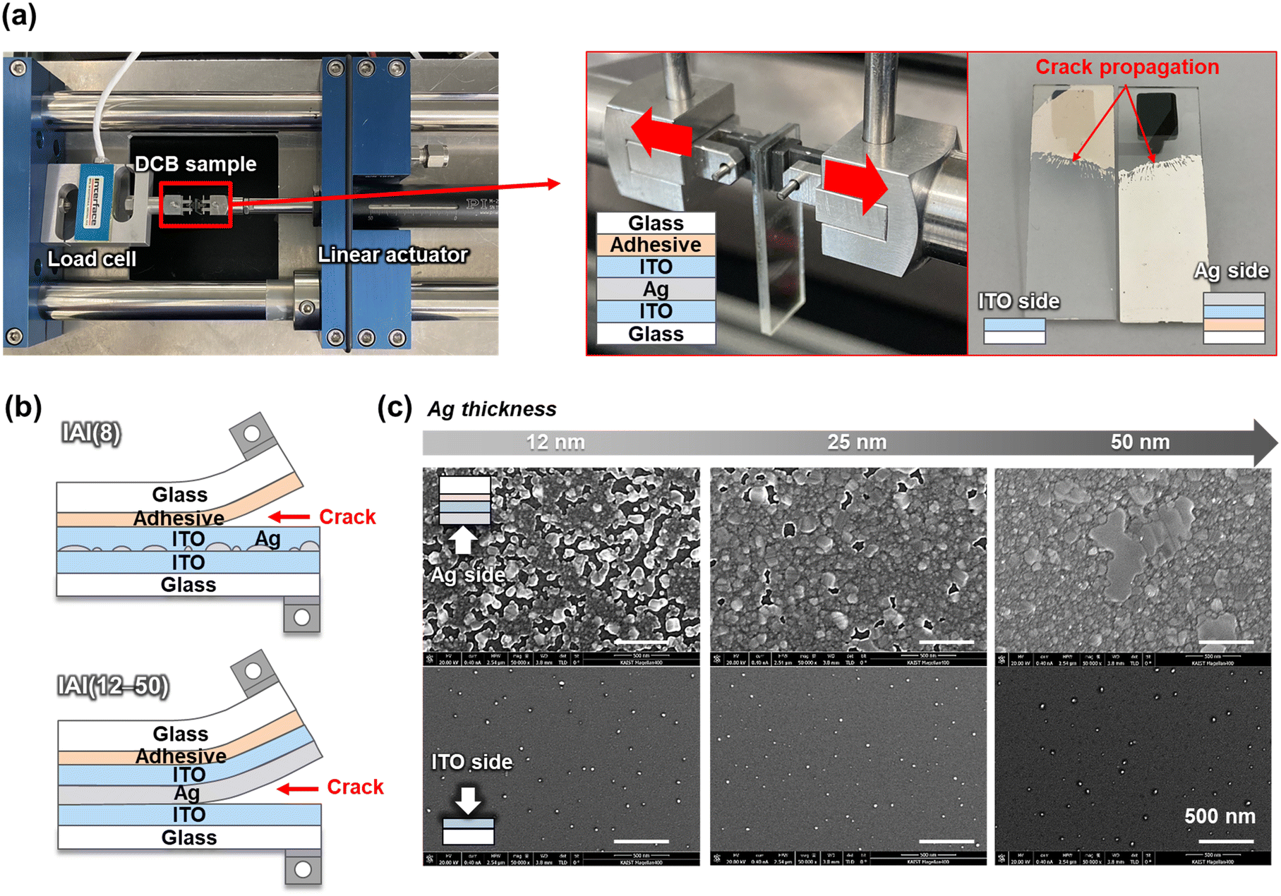 | ||
| Fig. 4 DCB testing method for the IAI thin films and resultant delaminated surfaces. (a) Photo of the DCB equipment and a representative delaminated IAI (25) specimen. (b) Illustrations of the resultant crack pathway depending on Ag thickness. Interlayers of the IAI(8) specimens were not delaminated and interfacial fracture occurred for the IAI(12–50) specimens. (c) SEM images of the delaminated surface morphologies as a function of Ag thickness. | ||
Based on the results of the tensile test, SEM analysis, and DCB test, the function of the Ag interlayer formation in the tensile and fracture behavior of the IAI thin films is proposed. As illustrated in Fig. 5, the Ag islands in IAI(8) thin films act as a point nucleation site for the top ITO, resulting in the formation of a distinct columnar microstructure. In this case, the density-deficient boundaries of the columnar structure of the top ITO serve as critical defect sites, leading to poor mechanical properties of the IAI thin films. For IAI(10–14), the film-like Ag interlayer functions as a plane nucleation site for the top ITO, contributing to the formation of a denser structure. This leads to a reduction in the voids at the boundary of the columnar ITO structure and thus, improves the mechanical properties of the IAI thin films. Additionally, the Ag interlayer covers the boundaries of the ITO particles, reducing stress concentration. Therefore, the densified Ag interlayer and reduced voids at ITO boundaries, in combination, significantly increase the Young's modulus and elongation. Additionally, IAI(25, 50) thin films with a film-type Ag interlayer show a decreased Young's modulus owing to the increased proportion of the Ag layer and deteriorated elongation caused by the formation of grain boundaries as a result of the crystallization of the Ag layer into larger agglomerates. In the future, exploring the mechanical properties of IAI thin films with controlled wetting characteristics of the Ag interlayer would be beneficial for gaining a better understanding of how to design the functional multilayer thin films.
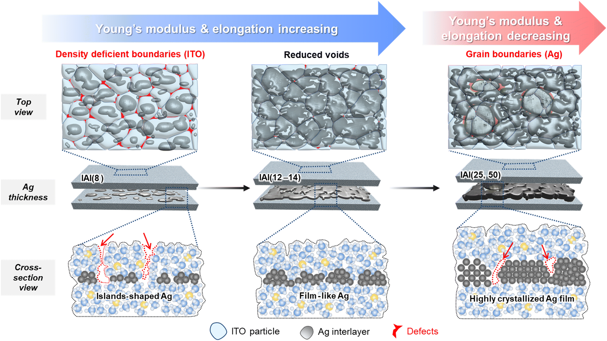 | ||
| Fig. 5 Schematic of the structural changes in the IAI thin films as a function of Ag interlayer formation. The effect of the Ag interlayer and the associated mechanical properties of the IAI thin films is proposed. | ||
Mechanical, electrical, and optical optimization toward robust thin film electrodes
The optical and electrical properties of the as-prepared IAI thin films are shown in Fig. 6 and Table S2 (ESI†). Fig. 6a shows representative samples of the IAI(8), IAI(12), IAI(25), and IAI(50) thin films deposited onto soda-lime glass substrates. As shown in Fig. 6b and c, the optical transmittance was the highest (83.2%) for an Ag thickness of 12 nm. The sheet resistance of the as-deposited IAI thin films as a function of Ag thickness is plotted in Fig. 6c. The sheet resistance rapidly decreased from 110.5 ± 4.6 Ω sq−1 to 1.63 ± 0.04 Ω sq−1 as the Ag thickness increased, as previously reported in the literature.15 The thin films exhibited high optical transmittance (>80% in the visible range) and low sheet resistance (<15 Ω sq−1), indicating their potential for use as transparent electrodes in flexible electronic devices. At the initial stage of the Ag film formation, discontinuous Ag islands are formed according to the Volmer–Weber growth mode, which is known to have a negative effect on conductivity owing to the comparable thickness to the electron mean free path (MFP).54 As the deposition progresses, these islands grow and percolate to form a semicontinuous/conductive film, thereby the sheet resistance significantly decreases. To select an efficient TCE, the figure of merit is a key parameter that represents the optical and electrical performance of a film. By correlating the transmittance measured at a wavelength of 550 nm and the sheet resistance, the figure of merit of the IAI thin films with varying Ag thicknesses was calculated, as defined by Haacke:| ϕ = T10/Rs | (2) |
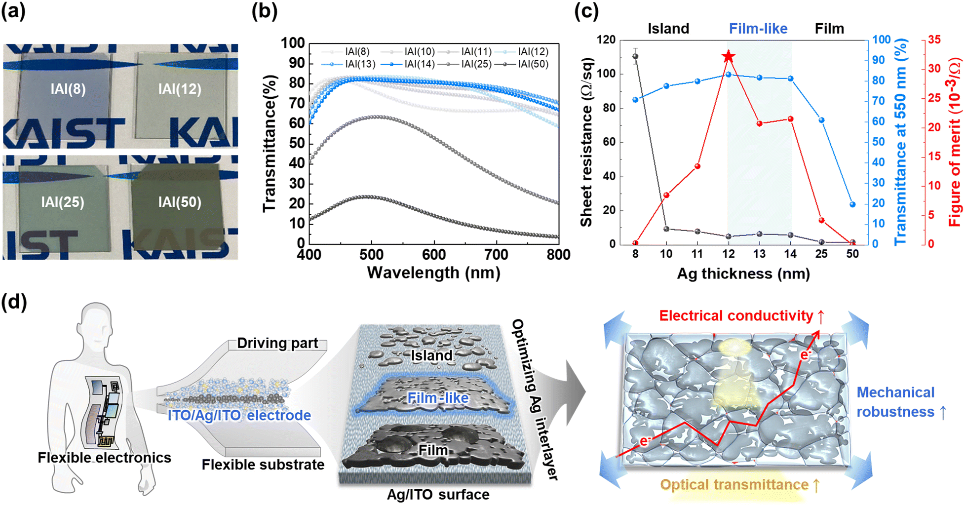 | ||
| Fig. 6 Optical and electrical characterization for the IAI thin films as a function of Ag thickness. (a) Photograph showing the difference in the transmittance of the IAI(8), IAI(12), IAI(25), and IAI(50) thin films on the glass substrate. (b) UV-Vis spectra of the IAI thin films. The IAI(12–14) thin films exhibited higher optical transmittance among the films. (c) Sheet resistance, representative transmittance at 550 nm, and figure of merit of the IAI thin films with different Ag thicknesses. (d) Insight on optimizing the Ag interlayer formation for robust design of advanced flexible electronics. | ||
The IAI(12) film exhibited the highest figure of merit (32.2 × 10⁻³ Ω), which is comparable with reported as-deposited IAI thin films.15,55–57 Thus, using the low-temperature process without any substrate heating or post-annealing steps, IAI thin films with a high optical transmittance and low sheet resistance were obtained. Overall, it has been discovered that the film-like formation of the Ag interlayer in IAI thin films plays a crucial role in achieving optimal mechanical, electrical, and optical performance (Fig. 6d).
Experimental section
Materials and sample preparation
Femtosecond laser patterning
The sputtered ITO thin film on the Cu/SiO2/Si substrate was fabricated in a dog-bone shape using a femtosecond laser (Pharos, L2K Co., Korea). The pulse power (10 mW) and frequency (100 kHz) of the laser were optimized to cut the ITO and sacrificial Cu layers, which was required for the clear separation of the dog-bone-shaped specimen. The total, grip section, and gage lengths of the fabricated dog-bone specimens were 17.2, 5, and 10 mm, respectively. Additionally, the widths of the grip and reduced sections were 5 and 0.8 mm, respectively (Fig. S9, ESI†).Free-standing tensile test
A water surface with a high surface tension (73 mN m−1) and low viscosity (1.002 mPa s−1) was used as a platform to fabricate the IAI thin films in a free-standing state.30 On the left and right sides of the free-standing IAI thin film, a high-resolution load cell (LTS-50GA, KYOWA, Japan) and linear actuator (M-111.1DG, PI, Germany) were placed on an anti-vibration table (Fig. S5, ESI†). For the tensile test, load values were acquired using the load cell, and in situ strain values were obtained using a DIC system with a charge-coupled device (CCD) camera. After gripping the IAI thin film with PDMS-coated Si grips, the tensile test was conducted at a strain rate of ∼5.8 × 10⁻⁵ s−1. The tensile test environment was uniformly maintained at a room temperature of 25 °C and relative humidity (RH) of approximately 20%. For the IAI thin films as a function of Ag thickness, 3–5 samples were evaluated among the fabricated 10–20 samples. The representative free-standing tensile test results show highly reproducible curves (Fig. S10, ESI†).Characterization of the ITO thin films
After the tensile test, the IAI thin films were transferred onto a Si substrate to measure the thickness of each film using atomic force microscopy (Park Systems, XE-100, Korea). Before transfer, the IAI thin films were rinsed with deionized water immediately after the tensile test to dilute the residual ammonium persulfate solution. The scanned area (20 × 5 μm) was measured at a scan frequency of 0.4 Hz, and the thickness was determined by measuring the height gap between the Si substrate and IAI thin film. The crystallographic state of the IAI thin films was characterized by X-ray diffractometer (Ultima IV, RIGAKU, Japan) with Cu radiation (λ = 1.5406 Å). A 2θ measurement with an initial inclination angle of 2° was conducted to amplify the reflection peaks of the IAI film. Additionally, the microstructures of the IAI thin films were characterized by scanning electron microscopy (Magellan 400, FEI Co., USA) at an accelerating voltage of 10–20 kV. To quantitatively determine the optical and electrical performances of the IAI thin films, the transmittance was characterized by ultraviolet/visible/near infrared (UV-VIS/NIR) spectroscopy (Lambda 1050, PerkinElmer, Korea) and a four-point probe was used to measure the sheet resistance of the IAI thin films depending on the Ag thickness.Double cantilever beam (DCB) test
The DCB test was performed to evaluate the fracture energy of the IAI interfaces and characterize the surface morphology of the Ag interlayer (Fig. S11, ESI†). The DCB specimens were fabricated into a sandwich structure by joining glass substrates on the IAI/glass substrates using a brittle-type epoxy (Epo-Tek 353ND, Epoxy Technology, USA). The epoxy was cured at room temperature (∼25 °C) for 72 h to prevent thermal damage to low-temperature-processed IAI thin films. A delaminator (Delaminator Adhesion Test System; DTS Company, USA) was used for the DCB test, which consisted of a load cell (SSM-FDH 200 N, Interface, USA), linear actuator (M-235.5DG, PI, Germany), and loading grips. The DCB tests were conducted at room temperature (∼25 °C) under controlled RH (∼30%).Conclusions
In summary, our findings demonstrate the importance of controlling the Ag interlayer formation in IAI thin films to achieve superior mechanical, structural, optical, and electrical properties. According to the tensile test results, Ag interlayer formation in a film-like structure (12–14 nm) exhibited optimum mechanical properties. The resulting films showed approximately a two-fold increase in both elongation (0.54–0.56%) and tensile strength (480.0–514.3 MPa) compared to the reference ITO thin film. The superior mechanical properties observed in the films can be attributed to the film-like formation of the Ag interlayer, which reduces defects and covers voids between the boundaries of the ITO particles. On the other hand, island-type Ag (8 nm) induces distinct columnar growth of the top ITO with density-deficient boundaries, and the film-type Ag (25, 50 nm) has grain boundaries along the Ag crystallites, which act as critical defects. Consequently, the use of IAI thin films with a film-like Ag interlayer that exceeds the island-type Ag layer is crucial to simultaneously enhance the mechanical robustness, electrical performance, and transparency for a variety of advanced flexible electronic applications.Author contributions
S. J. O, J. H. K., and T.-S. K conceived and designed the experiments and prepared the manuscript. J. H. K fabricated the ITO/Ag/ITO (IAI) multilayer thin films used in the study. S. J. O conducted the IAI thin film free-standing tensile test and double cantilever beam test. S. J. O and S. L analyzed the results. All authors discussed the results and commented on the manuscript.Conflicts of interest
There are no conflicts to declare.Acknowledgements
This study was supported by the National Research Foundation of Korea (NRF) funded by the Korean Government (MSIT) (Grant no. 2022R1A2C3009087 and 2022R1F1A1075914) and by the NRF grant for the Wearable Platform Materials Technology Center (WMC) funded by the MSIT (Grant no. 2022R1A5A6000846). This study was also supported by the KAIST Grand Challenge 30 Project (Grant no. N11210198). This study was supported by “Regional Innovation Strategy (RIS)” through the NRF funded by the Ministry of Education (MOE)(2021RIS-004). In addition, this study was supported by the Technology Innovation Program (20018379, Development of high-reliability light-emitting fiber-based woven wearable displays) funded By the Ministry of Trade, Industry & Energy (MOTIE, Korea).References
- H. Kim, J. S. Horwitz, G. Kushto, A. Pique, Z. H. Kafafi, C. M. Gilmore and D. B. Chrisey, J. Appl. Phys., 2000, 88, 6021–6025 CrossRef CAS
.
- Y. C. Lin, J. Y. Li and W. T. Yen, Appl. Surf. Sci., 2008, 254, 3262–3268 CrossRef CAS
- V. Teixeira, H. N. Cui, L. J. Meng, E. Fortunato and R. Martins, Thin Solid Films, 2002, 420, 70–75 CrossRef
- C. H. Hsu, Z. X. Zhang, C. Y. Shi, P. H. Huang, W. Y. Wu, D. S. Wuu, P. Gao, C. J. Huang, S. Y. Lien and W. Z. Zhu, J. Mater. Chem. C, 2022, 10, 12350–12358 RSC
- C. C. Lee, C. J. Shih, G. Kumar, S. Biring, S. Sen and S. W. Liu, J. Mater. Chem. C, 2017, 5, 12050–12056 RSC
- S. M. Lee, H. W. Koo, T. W. Kim and H. K. Kim, Surf. Coat. Technol., 2018, 343, 115–120 CrossRef CAS
- C. Peng, Z. Jia, D. Bianculli, T. Li and J. Lou, J. Appl. Phys., 2011, 109, 103530 CrossRef
- H. L. Wang, C. M. Tang, Q. Shi, M. Y. Wei, Y. F. Su, S. S. Lin and M. J. Dai, Ceram. Int., 2021, 47, 7666–7673 CrossRef CAS
- K. J. Ko, S. R. Shin, H. B. Lee, E. Jeong, Y. J. Yoo, H. M. Kim, Y. M. Song, J. Yun and J. W. Kang, Mater. Today Energy, 2021, 20, 100704 CrossRef CAS
- Y. L. Zhang, Z. Liu, C. G. Ji, X. L. Chen, G. F. Hou, Y. L. Li, X. Zhou, X. H. Cui, X. F. Yang, C. C. Ren, D. Liu, L. J. Guo, Y. Zhao and X. D. Zhang, ACS Appl. Energy Mater., 2021, 4, 6553–6561 CrossRef CAS
- C. C. Wu, Rsc. Adv., 2018, 8, 11862–11870 RSC
- Y. Kim, G. J. Jeon, M. K. Lee, S. H. Lee and S. H. K. Park, ECS Trans., 2016, 75, 247–251 CrossRef CAS
- J. H. Kwon, J. Park, M. K. Lee, J. W. Park, Y. Jeon, J. Bin Shin, M. Nam, C. K. Kim, Y. K. Choi and K. C. Choi, ACS Appl. Mater. Interfaces, 2018, 10, 15829–15840 CrossRef CAS PubMed
- W. Y. Ji, T. Wang, B. Y. Zhu, H. Zhang, R. Wang, D. D. Zhang, L. Z. Chen, Q. Y. Yang and H. Z. Zhang, J. Mater. Chem. C, 2017, 5, 4543–4548 RSC
- N. Ren, J. Zhu and S. Ban, AIP Adv., 2017, 7, 055009 CrossRef
- S. H. Park, S. J. Lee, J. H. Lee, J. Kal, J. Hahn and H. K. Kim, Org. Electron., 2016, 30, 112–121 CrossRef CAS
- M. Girtan and B. Negulescu, Opt. Mater.: X, 2022, 13, 100122 CAS
- C. Guillen and J. Herrero, Sol. Energy Mater. Sol. Cells, 2008, 92, 938–941 CrossRef CAS
- J. A. Jeong and H. K. Kim, Sol. Energy Mater. Sol. Cells, 2009, 93, 1801–1809 CrossRef CAS
- W. Y. Yang, Y. Gong, C. Y. Yao, M. Shrestha, Y. Y. Jia, Z. Qiu, Q. H. Fan, A. Weber and W. Li, Lab Chip, 2021, 21, 1096–1108 RSC
- T. H. Kim, S. H. Park, D. H. Kim, Y. C. Nah and H. K. Kim, Sol. Energy Mater. Sol. Cells, 2017, 160, 203–210 CrossRef CAS
- S. Park, J. Yoon, S. Kim and P. Song, RSC Adv., 2021, 11, 3439–3444 RSC
- I. Baia, M. Quintela, L. Mendes, P. Nunes and R. Martins, Thin Solid Films, 1999, 337, 171–175 CrossRef CAS
- B. Tyagi, H. B. Lee, N. Kumar, W. Y. Jin, K. J. Ko, M. M. Ovhal, R. Sahani, H. J. Chung, J. Seo and J. W. Kang, Nano Energy, 2022, 95, 106978 CrossRef CAS
- J. H. Song, J. W. Jeon, Y. H. Kim, J. H. Oh and T. Y. Seong, Superlattices Microstruct., 2013, 62, 119–127 CrossRef CAS
- K. P. Sibin, N. Selvakumar, A. Kumar, A. Dey, N. Sridhara, H. D. Shashikala, A. K. Sharma and H. C. Barshilia, Sol. Energy, 2017, 141, 118–126 CrossRef CAS
- E. H. Ko, H. J. Kim, S. J. Lee, J. H. Lee and H. K. Kim, RSC Adv., 2016, 6, 46634–46642 RSC
- H. Ferhati, F. Djeffal and A. Benhaya, Superlattices Microstruct., 2019, 129, 176–184 CrossRef CAS
- M. Y. Wang, A. Barnabe, Y. Thimont, J. M. Wang, Y. C. He, Q. R. Liu, X. L. Zhong, G. B. Dong, J. M. Yang and X. G. Diao, Electrochim. Acta, 2019, 301, 200–208 CrossRef CAS
- J. H. Kim, A. Nizami, Y. Hwangbo, B. Jang, H. J. Lee, C. S. Woo, S. Hyun and T. S. Kim, Nat. Commun., 2013, 4, 2520 CrossRef PubMed
- S. J. Oh, J. H. Kwon, S. Lee, K. C. Choi and T. S. Kim, ACS Appl. Mater. Interfaces, 2021, 13, 16650–16659 CrossRef CAS PubMed
- C. H. Lee, J. H. Kim, C. Y. Zou, I. S. Cho, J. M. Weisse, W. Nemeth, Q. Wang, A. C. T. Van Duin, T. S. Kim and X. L. Zheng, Sci. Rep., 2013, 3, 2917 CrossRef PubMed
- S. J. Oh, B. S. Ma, C. H. Yang and T. S. Kim, ACS Appl. Electron. Mater., 2022, 4, 3980–3987 CrossRef CAS
- J. H. Kim, K. L. Jang, K. Ahn, T. Yoon, T. I. Lee and T. S. Kim, Sci. Rep., 2019, 9, 7071 CrossRef PubMed
- T. I. Lee, W. Jo, W. Kim, J. H. Kim, K. W. Paik and T. S. Kim, ACS Appl. Mater. Interfaces, 2019, 11, 13416–13422 CrossRef CAS PubMed
- J. Yoon, Y. Jang, K. Kim, J. Kim, S. Son and Z. Lee, Carbon, 2022, 196, 236–242 CrossRef CAS
- H. Mizubayashi, J. Matsuno and H. Tanimoto, Scr. Mater., 1999, 41, 443–448 CrossRef CAS
- R. Long and M. L. Dunn, J. Appl. Phys., 2014, 115, 233514 CrossRef
- M. Gu, W. J. Song, J. Hong, S. Y. Kim, T. J. Shin, N. A. Kotov, S. Park and B. S. Kim, Sci. Adv., 2019, 5, eaaw1879 CrossRef CAS PubMed
- J. Yun, Adv. Funct. Mater., 2017, 27, 1606641 CrossRef
- M. Volmer, Z. Phys. Chem., 1926, 119, 277–301 CrossRef CAS
- L. Vj, N. P. Kobayashi, M. S. Islam, W. Wu, P. Chaturvedi, N. X. Fang, S. Y. Wang and R. S. Williams, Nano Lett., 2009, 9, 178–182 CrossRef PubMed
- X. Yang, P. Gao, Z. Yang, J. Zhu, F. Huang and J. Ye, Sci. Rep., 2017, 7, 44576 CrossRef CAS PubMed
- T. Lee, D. Kim, M. E. Suk, G. Bang, J. Choi, J. S. Bae, J. H. Yoon, W. J. Moon and D. Choi, Adv. Funct. Mater., 2021, 31, 2104372 CrossRef CAS
- J. S. Kim, R. H. Friend and F. Cacialli, J. Appl. Phys., 1999, 86, 2774–2778 CrossRef CAS
- H. S. Im, S. K. Kim, T. J. Lee and T. Y. Seong, Vacuum, 2019, 169, 108871 CrossRef CAS
- W. J. Dong, H. K. Yu and J. L. Lee, Sci. Rep., 2020, 10, 12819 CrossRef CAS PubMed
- P. Buffat and J. P. Borel, Phys. Rev. A: At., Mol., Opt. Phys., 1976, 13, 2287–2298 CrossRef CAS
- S. R. Foltyn, L. Civale, J. L. Macmanus-Driscoll, Q. X. Jia, B. Maiorov, H. Wang and M. Maley, Nat. Mater., 2007, 6, 631–642 CrossRef CAS PubMed
- S. Tsukimoto, M. Moriyama and M. Murakami, Thin Solid Films, 2004, 460, 222–226 CrossRef CAS
- M. L. Chang, L. C. Wang, H. C. Lin, M. J. Chen and K. M. Lin, Appl. Surf. Sci., 2015, 359, 533–542 CrossRef CAS
- A. Lazauskas, V. Grigaliunas, A. Guobiene, M. Andrulevicius and J. Baltrusaitis, Thin Solid Films, 2012, 520, 6328–6333 CrossRef CAS
- P. J. Martin, Gold Bull., 1986, 19, 102–116 CrossRef CAS
- Y. L. Cha, J. H. Jo, D. J. Kim and S. H. Kim, Nanomaterials, 2022, 12, 2060 CrossRef CAS PubMed
- C. Guillen and J. Herrero, Opt. Commun., 2009, 282, 574–578 CrossRef CAS
- Y. S. Park, K. H. Choi and H. K. Kim, J. Phys. D: Appl. Phys., 2009, 42, 235109 CrossRef
- J. H. Kim, T. W. Kang, S. N. Kwon, S. I. Na, Y. Z. Yoo, H. S. Im and T. Y. Seong, J. Electron. Mater., 2017, 46, 306–311 CrossRef CAS
Footnote |
| † Electronic supplementary information (ESI) available. See DOI: https://doi.org/10.1039/d3tc01002c |
| This journal is © The Royal Society of Chemistry 2023 |