
Interfacial defect healing of In2S3/Sb2(S,Se)3 heterojunction solar cells with a novel wide-bandgap InOCl passivator†
Changxue
Wang
ab,
Dongdong
Li
c,
Xiaoli
Mao
b,
Lei
Wan
a,
Zhen
Cheng
a,
Jun
Zhu
 d,
Robert L. Z.
Hoye
e and
Ru
Zhou
*ae
d,
Robert L. Z.
Hoye
e and
Ru
Zhou
*ae
aSchool of Electrical Engineering and Automation, Hefei University of Technology, Hefei 230009, P. R. China. E-mail: zhouru@hfut.edu.cn
bSchool of Microelectronics, Hefei University of Technology, Hefei 230009, P. R. China
cSchool of Materials Science and Engineering, Hefei University of Technology, Hefei 230009, P. R. China
dAcademy of OptoElectric Technology, Hefei University of Technology, Hefei 230009, P. R. China
eInorganic Chemistry Laboratory, Department of Chemistry, University of Oxford, South Parks Road, Oxford OX1 3QR, UK
First published on 21st July 2023
Abstract
In2S3 has been regarded as a promising nontoxic alternative to CdS as an n-type electron transporting layer (ETL) for environmentally friendly antimony chalcogenide solar cells. However, the high-density of vacancy defects in In2S3 cause severe interfacial charge recombination in optoelectronic devices. To tackle this issue, herein we successfully incorporate a novel structurally two-dimensional wide-bandgap InOCl as an interfacial passivator between the In2S3 buffer layer and Sb2(S,Se)3 absorber through a simple InCl3 post-treatment strategy, which effectively improves the quality of the In2S3/Sb2(S,Se)3 heterointerface. Through careful experimental and computational studies, we believe that the wide bandgap InOCl passivator plays an important role in defect healing of In2S3 at the heterointerface by increasing the vacancy formation energy and thus reducing the density of defect states. Moreover, this interfacial layer contributes to the formation of a more favorable “spike”-like energy band alignment at the ETL/absorber interface and inhibits the transformation of In2S3 into In(OH)3 in moist air. As a result of significantly suppressed detrimental effects from interfacial recombination via positive defect healing, the In2S3/InOCl-based Sb2(S,Se)3 solar cell obtains a remarkable power conversion efficiency of 5.20%. To the best of our knowledge, this is the champion efficiency reported for In2S3-based antimony chalcogenide solar cells.
1. Introduction
Renewable solar energy affords an effective solution for energy and environmental issues all around the world. A variety of semiconductor photovoltaic materials have been explored for high efficiency photovoltaics, such as silicon, cadmium telluride (CdTe), copper–indium–gallium–selenium (CIGS), lead-halide perovskites, etc.1–4 Promising antimony chalcogenides, including Sb2S3, Sb2Se3, and alloyed Sb2(S,Se)3, have received tremendous attention due to their excellent materials and optoelectronic properties, such as a high absorption coefficient (∼105 cm−1), a tunable band gap (1.1–1.7 eV), abundant and non-toxic compositions, ease of fabrication, outstanding material stability, etc. Such merits allow for great prospects for antimony chalcogenide solar cells.5–7 In recent years, thanks to great efforts devoted to new-processing-method exploration, interfacial engineering, crystal orientation control, ion doping, etc., the record power conversion efficiency (PCE) of antimony chalcogenide photovoltaics has been pushed up to 10.7%.7 Generally, high performance antimony chalcogenide solar cells adopt the n–i–p device configuration, in which the n-type electron transport layer (ETL) plays a critical role in extracting photogenerated electrons from absorbers and then transporting them to the electrode.8,9 To date, the compact CdS buffer layer has been widely used as an inorganic ETL for thin film photovoltaics because of its high electron mobility.8,10–12 However, the use of CdS for thin film solar cells imposes severe environmental pollution problems due to the presence of toxic Cd, thereby calling for Cd-free substitute buffer layer materials, such as TiO2, SnO2, ZnO, In2S3, etc. It is worth mentioning that, besides forming a heterojunction with the absorber for the separation of carriers, the ETL also serves as a growth matrix for the deposition of functional layers.11,13 That is, the ETL substrate significantly influences the subsequent deposition of absorber films; the compatibility between ETL/hole transporting layer (HTL) and absorber materials should also be taken into consideration.11,14–16 For antimony chalcogenide solar cells, it is difficult to deposit high-quality compact absorber films with preferred orientation onto oxide buffer layers by using conventional chemical bath deposition (CBD) or hydrothermal deposition approaches, thereby delivering quite poor device efficiencies.10 Among various Cd-free ETL candidates, sulfur-based In2S3 is suggested to be a promising one for antimony chalcogenide solar cells.17,18Environmentally friendly In2S3 is an n-type III–VI semiconductor for optoelectronic applications, exhibiting excellent characteristics including a reasonable band gap (2.0–2.8 eV), high carrier mobility (17.6 cm2 V−1 s−1), controllable electrical properties, thermal and chemical stability, etc.18–22 In particular, regarding the low melting point of antimony chalcogenides (<400 °C), the low-temperature preparation of In2S3 thin films could enable the fabrication of flexible photovoltaic devices coupled with lightweight flexible polymer-based substrates such as polyimide (PI), polyethylene naphthalate (PEN), etc. The comparison of material, optical, and electrical properties between In2S3 and other commonly used ETLs reveals the superior material and optoelectronic properties of In2S3 (Table S1†), verifying In2S3 to be a promising buffer layer-material for thin film solar cells to replace commonly used CdS. At present, In2S3 has been successfully utilized for CuInS2, Cu(In,Ga)Se2, and lead-halide perovskite solar cells, and achieved decent PCEs.18,20 However, up to now, there have been few studies on In2S3-based antimony chalcogenide photovoltaics, yielding efficiencies lagging far behind those of their CdS-based counterparts.23 The point to emphasize here is that most of these cases employ an In2S3 constructed double-layer ETL coupled with other materials, such as CdS, TiO2, etc.17,24–26 For example, Huerta-Flores et al. deposited an In2S3 layer on TiO2 by using successive ionic layer adsorption and reaction method, obtaining 4.9%-efficient Sb2S3 solar cells.24
The moderate device efficiency for In2S3-based antimony chalcogenide solar cells might be closely associated with a high density of vacancy defects of In2S3 materials. In2S3 has three stable crystallographic phases: α-In2S3 with a defective cubic structure, β-In2S3 with a defective spinel structure that has either a tetragonal or cubic unit cell, and γ-In2S3 with a layered hexagonal structure.27–29 Among these three crystal structures, β-In2S3 is the most favorable phase for optoelectronic applications. β-In2S3 is a stable phase at room temperature which crystallizes in a defect spinel lattice having a high degree of In vacancies at tetrahedral cation sites. In the spinel lattice structure of β-In2S3, In3+ centers are surrounded by six S2− in octahedral sites and four S2− in tetrahedral sites; the octahedral sites are fully occupied with cation centers, while 2/3 of the tetrahedral sites are occupied, with the remaining 1/3 empty, forming In3+ vacancies.21,27,28,30 Such In vacancy sites will act as electron traps. The ordered modification of the β-In2S3 phase is therefore interpreted as a quasi-ternary compound consisting of In, S and vacancies in a unit cell because of the presence of a great number of natural defects in crystals. Moreover, a number of vacancy-related energy states and surface states, coming from vacancies and self-interstitial and antisite defects, are found near the band edges in bulk β-In2S3, through theoretical prediction and experimental studies.29,31 High-density defects would cause severe defect-induced charge recombination in In2S3 films, especially at the ETL/absorber interface, thereby restricting the performance improvement of In2S3-based optoelectronic devices. Therefore, effective defect healing via interface engineering is of great importance for constructing a high-quality heterojunction to facilitate charge separation and transport. Wide bandgap materials have been reported to be capable of passivating surface structural defects. For example, for silicon technology, wide-bandgap oxides and nitrides, such as silicon oxide, silicon nitride, or aluminum oxide are often utilized to form strong covalent bonds with silicon which will protect the underlying silicon from degradation.32–34 For perovskite solar cells, Yang et al. reported the use of a thin lead sulfate (PbSO4) layer that is electrically insulating to stabilize halide perovskite surfaces for solar cell operation.32 Therefore, the use of wide-bandgap barrier layers might also play a role in healing the interface defects at the In2S3/absorber junction and consequently improve the performance of solar cells. However, to date, no attempts have been implemented on the In2S3 buffer layer to reduce the number of surface defects.
In this work, we demonstrate for the first time that a novel wide bandgap InOCl interfacial layer incorporated between In2S3 buffer layer and Sb2(S,Se)3 absorber layer contributes to the effective defect healing of In2S3 buffer layers and suppresses interfacial charge recombination. This passivation strategy implemented on the In2S3 layer is similar to those effectively used in other types of photovoltaics. The wide-bandgap InOCl interfacial layer passivates the high degree of In2S3 surface defects by increasing the vacancy formation energy and thus reduces the density of defect states. The positive defect healing of the In2S3 buffer layer also improves the heterojunction quality of solar cells. Thanks to the effective defect healing effect of the InOCl passivator, the corresponding In2S3-based antimony chalcogenide solar cells receive greatly improved photovoltaic performance.
2. Results and discussion
The In2S3 buffer layers were deposited on the conducting fluorine-doped tin oxide (FTO) substrate by using the chemical bath deposition (CBD) strategy. We first optimized the morphology and thickness of In2S3 films by changing the CBD duration. With an increase in the CBD time from 45 to 55, 65, and 75 min, the morphology of In2S3 films evolves from rough clusters to uniform nanosheets (Fig. S1, ESI†). Such a morphology evolution process can be explained by using classical nucleation theory.20 The formation of In2S3 films involves two processes, i.e., the initial nucleation followed by the gradual growth of In2S3 nanocrystals. Specifically, InCl3 and CH3CSNH2 acts as the In and S sources, respectively, while citric acid acts as the complexing agent. At the initial stage, citric acid and In3+ form a metal complex and CH3CSNH2 produces S2− in the acid environment; the slow release of In3+ and S2− ions results in the subsequent condensation and heterogeneous nucleation of In2S3 on the substrate when the ionic product of In3+ and S2− exceeds the solubility-product constant Ksp for In2S3 (∼5.7 × 10−73).35 The nuclei grown on the substrate form nanospheres composed of nanosheets. With an increase in deposition time, such nanospheres gradually vanish and evolve into nanosheets, finally forming a uniform network-like structure with a certain film thickness. Similar surface morphologies of In2S3 films have also been reported by Yang et al.20 The gradual growth of In2S3 films results in the formation of a nanosheet-constructed porous network structure. In particular, the In2S3 films prepared by 65 min-CBD display uniform and compact morphology features, being quite suitable for subsequent deposition of absorber films. Cross-sectional scanning electron microscopy (SEM) images (Fig. S1e–h, ESI†) further reveal that the film thickness is 124, 173, 235, and 290 nm at a CBD time of 45 to 55, 65, and 75 min, respectively.The X-ray diffraction (XRD) patterns (Fig. S2a, ESI†) demonstrate that the as-deposited In2S3 films on the FTO substrate present poor crystallization as reflected by quite weak and broad diffraction peaks. As for the In2S3 samples deposited under 65 min or longer, two diffraction peaks located at 27.4° and 48.0°, corresponding to the (311) and (440) planes of stable cubic β-In2S3 (JCPDS #65-0459), can be resolved.27,36,37 This fact indicates the successful deposition of In2S3 buffer layers on the substrate. A similar poor crystallinity characteristic for CBD-deposited In2S3 films was reported in the literature, and this might be associated with the presence of In–OH terminal bonds that block the formation of In–S–In bonds.37 This is further confirmed by X-ray photoelectron spectroscopy (XPS) later which reveals the existence of In–OH bonds. Moreover, we further collected the precipitates during the CBD process from the beaker and conducted XRD characterization to further reveal the crystal phase of In2S3 (Fig. S2b, ESI†). It is revealed that both of the precipitate samples processed without or with further annealing (300 °C, N2) exhibit obvious characteristic peaks for cubic β-In2S3. The transmittance spectra of In2S3 films processed at different CBD durations (Fig. S2c, ESI†) indicate that In2S3 films exhibit >70% over wavelengths longer than 550 nm. The high transmittances of In2S3 films are beneficial for effective photon harvesting in photovoltaic devices. Moreover, the transmittance of films gradually decreases in the absorption wavelength range with increasing CBD time.
We constructed superstrate Sb2(S,Se)3 solar cells based on the device configuration of FTO/In2S3/Sb2(S,Se)3/spiro-OMeTAD/Au by using In2S3 buffer layers prepared at different CBD durations. The device photovoltaic parameters, including Voc, Jsc, FF and PCE, measured under 1-sun illumination (AM1.5G, 100 mW cm−2), each based on 12 devices, are given in the box charts (Fig. S3, ESI†). As shown, the device efficiency increases at first and then drops as the CBD time increases from 45 to 75 min. The Sb2(S,Se)3 solar cells prepared by 65 min-CBD exhibit optimal repeatability and performance, demonstrating an average PCE of 2.57% and the highest PCE of 2.96%. This might benefit from the relatively higher quality of 65 min-CBD In2S3 films, which affords uniform surface morphology and appropriate thickness for interface contact and heterojunction formation in solar cells. Here it is worth noting that the optimal thickness of In2S3 films for Sb2(S,Se)3 solar cells is thicker than a typical thickness of ∼60 nm for commonly used CdS ETLs in thin film solar cells, and this should be closely associated with the properties of materials and films, such as absorption coefficients, morphology, etc. For example, the nanosheet-constructed porous network structure of In2S3 films is not as compact as that of chemical bath deposited CdS films. Generally, such pristine In2S3-based Sb2(S,Se)3 solar cells still suffer from relatively poor performance parameters, especially low Jsc and FF. The limited device efficiencies might be closely associated with poor charge extraction and transport at the ETL/absorber interface due to the high-density defects of In2S3 as discussed in the Introduction. The effective passivation of such defects is expected to improve the heterojunction quality and further boost the device efficiency. Inspired by the post-treatment of CdS and TiO2 films by using CdCl2 and TiCl4 solutions, respectively, herein we try to conduct the post-treatment of In2S3 buffer layers by using InCl3 precursor solutions.12,38 In this work, we perform careful characterization of films and devices to reveal the particular effects of InCl3 post-treatment and underlying mechanisms.
Fig. 1a and b show top-view SEM images of In2S3 without and with the InCl3 treatment, respectively. Herein the In2S3 buffer layer is obtained by 65 min-CBD, which delivers the highest PCE for pristine In2S3-based Sb2(S,Se)3 solar cells. The concentration of InCl3 methanol precursor solution is 0.02 g mL−1. As shown, compared to the pristine In2S3 film, the InCl3 post-treated film involves the formation of a conformal coating layer on the In2S3 surface, affording a more uniform and compact surface topography. Atomic force microscopy (AFM) images (Fig. 1c and d) reveal a root mean square (RMS) roughness of 27.2 and 25.8 nm for In2S3 buffer layers without and with InCl3 treatment, respectively. The relatively reduced roughness with the InCl3 treatment is beneficial for the intimate interface contact between the buffer layer and the absorber. In addition, with the InCl3 concentration increasing from 0.01, 0.02, 0.04 to 0.08 g mL−1, the post-treatment leads to more and more significant surface morphology evolution, as reflected by the generation of additional nanoflakes on In2S3 films with the high-concentration post-treatment (Fig. S4, ESI†). The average size of additional nanoflakes gradually increases with the InCl3 concentration.
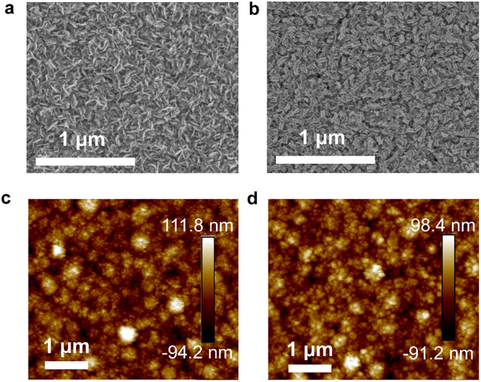 | ||
| Fig. 1 Top-view SEM and AFM images of In2S3 buffer layers (a and c) without InCl3 post-treatment and (b and d) with post-treatment by using 0.02 g mL−1 InCl3. | ||
After carefully examining the possible chemical reaction processes that occurred, we speculate that a product of the InCl3 post-treatment might be In2O3 or InOCl on the In2S3 surface. A series of characterization studies were then performed to elaborate this issue. The Raman spectra of In2S3 films without and with the InCl3 treatment (Fig. S5a, ESI†) reveal almost identical Raman spectra for both films, showing the characteristic peaks of In2S3.39,40 The prominent bands resolved as 244, 266, 306, and 366 cm−1 are attributed to the characteristic Raman peaks of cubic β-In2S3, consistent with the cases reported in the literature.39 The absorption spectra evidence the negligible influence of the InCl3 treatment on the absorbance and band gap of In2S3 (Fig. S5b, ESI†). Moreover, CBD-processed In2S3 is often demonstrated as a direct bandgap material, the effective optical bandgap of which can be estimated according to the Tauc plots as described by eqn (1):13,41–44
| (Ahυ)2 = c(hυ − Eg) | (1) |
Fig. 2a–d give X-ray photoelectron spectroscopy (XPS) spectra of In 3d, S 2p, O 1s, and Cl 2p of In2S3 buffer layers without and with the InCl3 post-treatment. As shown, the In 3d core level spectra of both samples present two main peaks at 452.6 and 445.0 eV, which correspond to In 3d3/2 and In 3d5/2, respectively.43,45 The spectrum deconvolution reveals that both spectra of S 2p exhibit two peaks located at 162.5 eV for S 2p1/2 and 161.3 eV for S 2p3/2 with a peak separation of ∼1.2 eV, agreeing with binding energies of S 2p in sulfide phases.45 Moreover, the sharply reduced S 2p peak intensities for the InCl3 treated sample imply the successful coating of a thin layer of sulfur-free materials onto the In2S3 layer. The O 1s presents a main peak centered at ∼532.1 eV assigned to hydroxyl groups (OH−), manifesting the generation of In(OH)3 through the deliquescence of In2S3 in an atmospheric environment.43 The InCl3 post-treatment produces an additional new peak centered at a lower binding energy of ∼530.0 eV, and this characteristic peak serves as a fingerprint for the presence of lattice oxygen, which might arise from InOCl. Additionally, the remarkable reduced intensity from In(OH)3 species indicates that the InCl3 treatment is capable of inhibiting the transformation of In2S3 in moist air. The Cl 2p involves a couple of peaks at higher energies of 200.5 eV for Cl 2p1/2 and 198.8 eV for Cl 2p3/2; moreover, the comparison of Cl 2p peak intensity reflects that the InCl3 treatment produces Cl-containing materials on the In2S3 surface, echoing the formation of InOCl.
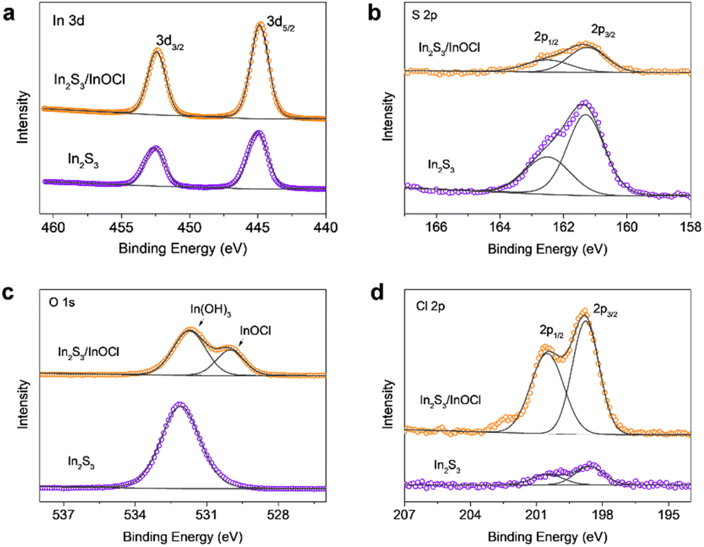 | ||
| Fig. 2 XPS spectra of (a) In 3d, (b) S 2p, (c) O 1s, and (d) Cl 2p of In2S3 buffer layers without and with the InCl3 post-treatment. | ||
The XRD, EDS and XPS results cross-validate the generation of InOCl materials on the In2S3 buffer layer. It is demonstrated that InCl3 is an inorganic compound that can easily degrade in moist air, whereas InOCl is stable up to 350 °C. Further increases in temperature would lead to the decomposition of InOCl into In2O3.46,47 Therefore, we believe that, in this work, the InCl3 post-treatment followed by annealing at 300 °C in an ambient atmosphere results in the formation of InOCl rather than In2O3. InOCl is known as a structurally two-dimensional (2D) layered material with layers stacked by van der Waals interactions.48,49 Hereinafter, we denote the In2S3 films without and with the InCl3 post-treatment and corresponding devices as “In2S3” and “In2S3/InOCl” samples.
We carried out density functional theory (DFT) calculations to study the interaction between In2S3 and InOCl and scrutinize the particular impacts of the InOCl interfacial layer. Surface structural modeling of the InOCl/β-In2S3 (110) interface after structural relaxation is shown in Fig. S7a in the ESI.† To evaluate the stability of the adsorption of the InOCl monolayer on the β-In2S3 (110) surface, the adsorption energy is defined as: Ea = Etot − EIn2S3(110) − EInOCl, where EIn2S3(110), EInOCl and Etot are the total energy of the In2S3 (110) surface, the InOCl monolayer, and the InOCl monolayer adsorbed on the In2S3 (110) surface, respectively. The adsorption energy of the InOCl monolayer on the β-In2S3(110) surface is −0.93 eV, indicating a strong electronic coupling and chemical binding between InOCl and In2S3. The InOCl monolayer is chemisorbed on β-In2S3 (110) via a strong chemical bond between Cl and In. Fig. 3a depicts the partial density of states (DOS) of In and Cl of the InOCl/In2S3 (110) interface. The Fermi levels (EF) of the system are set to 0 eV. Significant hybridizations between Cl 3p and In 5s and In 5p with an energy interval from −7.0 eV to 0 eV are observed. The isosurface of the electron density difference allows a more clear demonstration of the charge transfer. The charge density difference is drawn in Fig. 3b. The evident electron accumulation can be observed between Cl and In atoms because of the hybridizations, indicating that the InOCl monolayer has strong interactions with the In2S3 (110) surface. The vacancy formation energy of 4-fold In in the β-In2S3 (110) surface was also calculated and the results are given in Fig. 3c. The structural modeling of a 4-fold In vacancy at the InOCl/In2S3 (110) interface is shown in Fig. S7b in the ESI.† Herein the formation energies of the In vacancy in the β-In2S3 (110) surface are calculated according to the formula: Ef = EV+In2S3(110) + μIn − EIn2S3(110), where EIn2S3(110) and EV+In2S3(110) are the total energy of the β-In2S3 (110) surface and the total energy of the β-In2S3 (110) surface with an In vacancy inside, respectively. μIn is the chemical potential of In in a hexagonal close-packed (HCP) crystal. As shown, with the adsorption of the InOCl monolayer on the β-In2S3 (110) surface, the formation energy of the 4-fold In vacancy increased by 0.11–0.24 eV. This result means that the formation of the In vacancy becomes more difficult with the InOCl adsorption, implying the defect healing effect of the InOCl passivator. The lowered density of the In vacancy would contribute to suppressed charge recombination and more efficient charge transport.
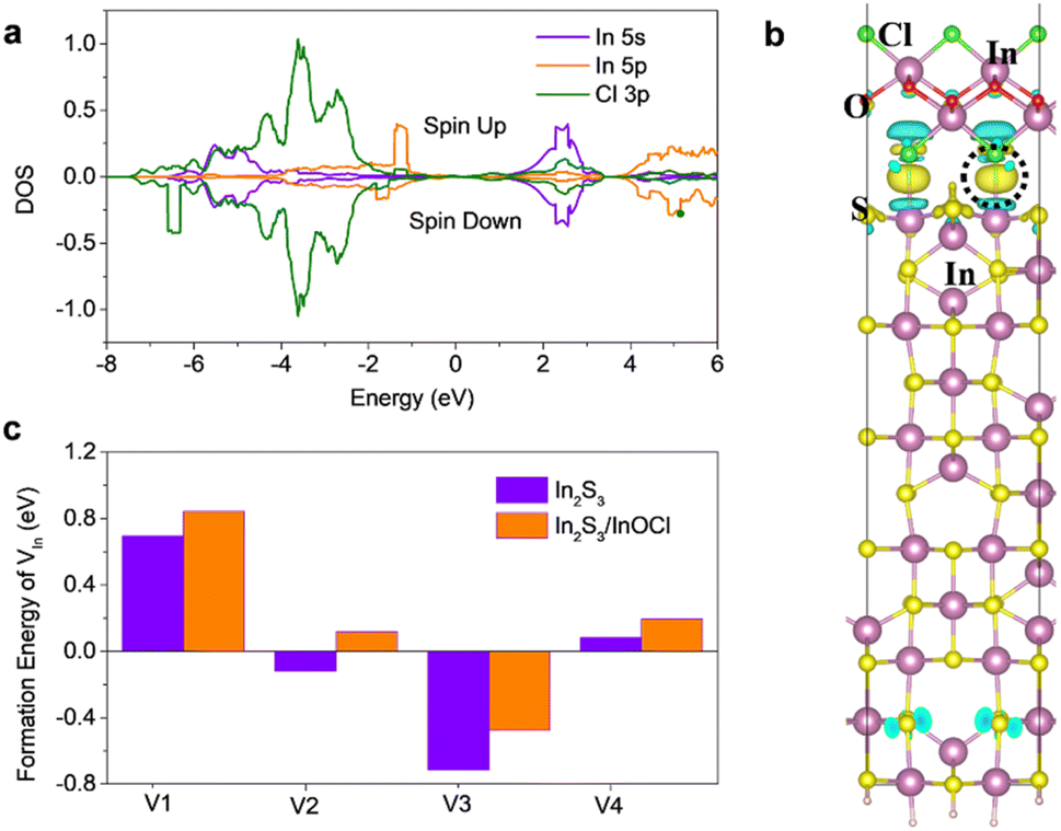 | ||
| Fig. 3 (a) DOS of In and Cl nearby for the InOCl dissociation on the β-In2S3 (110) surface. The positive and negative values represent spin-up and spin-down states, respectively. (b) The electron density difference of the InOCl/β-In2S3 (110) interface. The value of the isosurface is 0.0005 e Å−3. Yellow color and sky-blue colors represent the electron density increase and decrease, respectively. (c) The formation energy of a 4-fold In vacancy in β-In2S3 (110) with or without InOCl. | ||
XRD patterns of Sb2(S,Se)3 films deposited on In2S3 and In2S3/InOCl buffer layers (Fig. S8, ESI†) reveal that the hydrothermally deposited Sb2(S,Se)3 films exhibit strong diffraction peaks of 17.5°, 25.0°, 29.3° and 32.3° assigned to the (120), (130), (211), and (221) planes of a typical stibnite structure, respectively, reflecting the high crystallinity of the as-obtained absorber films.10,11 There are no additional diffraction peaks from any other impurity phases. The identical lattice structure of Sb2S3 and Sb2Se3 allows the facile formation of alloyed Sb2(S,Se)3 compounds.12,50 Compared to the standard card of Sb2S3 (JCPDS #42-1393), the diffraction peaks of alloyed Sb2(S,Se)3 shift to a lower 2-theta angle as a result of the increased lattice spacing by partially substituting S with larger Se.12,51 The nearly identical diffraction peaks for XRD patterns of different samples reveal that the InCl3 post-treatment has negligible impacts on the deposition of high-quality Sb2(S,Se)3 absorber films. The comparison of top-view and cross-sectional view SEM images of Sb2(S,Se)3 absorber films constructed on In2S3 and In2S3/InOCl buffer layers is given in Fig. S9, ESI†. Both Sb2(S,Se)3 absorber films present quite compact and uniform films free of pinholes, similar to hydrothermally deposited Sb2(S,Se)3 films on CdS buffer layers.12 Moreover, with the introduction of the InOCl layer, the absorber film exhibits larger grains with fewer boundary cracks, with some grain sizes exceeding 3 μm. Both absorber films exhibit a nearly identical thickness of around 280 nm. A careful examination reveals more intimate physical contact at the ETL/Sb2(S,Se)3 interface, as reflected by significantly reduced voids at the interface. These facts confirm that the presence of InOCl is beneficial to improve the quality of Sb2(S,Se)3 absorbers and reinforce the contact at the interface, which might be associated with the reduced surface roughness and improved surface chemistry of buffer layers. The absorption spectra of Sb2(S,Se)3 films deposited on In2S3 and In2S3/InOCl layers (Fig. S10a, ESI†) show that both samples show negligible change of absorbance over the entire absorption range, echoing that of the identical thickness for both Sb2(S,Se)3 films deposited on different buffer layers. According to the Tauc plots (Fig. S10b†), the effective optical bandgap of Sb2(S,Se)3 absorbers is estimated to be 1.54 eV, close to our previous results.10 The cross-sectional EDS line scan of Sb2(S,Se)3 solar cells demonstrates the uniform vertical distribution of Sb, S, Se, and In elements in absorber and buffer layers (Fig. S11a and b, ESI†). The surface EDS characterization of the FTO/In2S3/Sb2(S,Se)3 sample (Fig. S11c, ESI†) further reveals that the atomic ratio of S/(S + Se) is estimated to be 27.78%. The elemental mapping images of Sb, S, Se, and In (Fig. S11d–h, ESI†) display the homogeneous spatial element distribution of functional layers on the substrates.
Fig. 4a schematically illustrates a complete n–i–p structured device with a configuration of FTO/In2S3/InOCl/Sb2(S,Se)3/spiro-OMeTAD/Au. As shown in the cross-sectional SEM image in Fig. 4b, the thicknesses of In2S3/InOCl, Sb2(S,Se)3, spiro-OMeTAD, and Au are estimated to be 235, 310, 90, and 80 nm, respectively. We fabricated Sb2(S,Se)3 solar cells based on In2S3 buffer layers treated with different InCl3 concentrations. The box charts of performance parameters (Fig. S12, ESI†) reveal that the device efficiency increases at first and then decreases with an increase in the InCl3 concentration. As shown, the optimal PCE and reproducibility are obtained at an InCl3 concentration of 0.04 g mL−1. Fig. 4c gives the J–V curves of the best-performing devices based on In2S3 and In2S3/InOCl buffer layers. Table 1 summarizes the corresponding photovoltaic parameters derived from J–V curves. The In2S3-based device yields a Voc of 0.58 V, Jsc of 15.29 mA cm−2, FF of 29.71% and PCE of 2.62%; while the In2S3/InOCl-based device obtains a Voc of 0.59 V, Jsc of 19.13 mA cm−2, FF of 46.09% and PCE of 5.20%. That is, the InCl3 post-treatment achieves nearly 98% efficiency enhancement for Sb2(S,Se)3 solar cells. The prominent parameter differences for both devices lie in Jsc and FF. Moreover, the In2S3/InOCl-based device gives a smaller series resistance (Rs) of 9.24 Ω cm2 compared to 31.63 Ω cm2 for the In2S3-based device, with a larger shunt resistance (Rsh) of 171.00 Ω cm2 compared to 80.09 Ω cm2. To the best of our knowledge, the value of 5.20% is the champion efficiency reported for In2S3-based antimony chalcogenide solar cells. The incident photon-to-electron conversion efficiency (IPCE) of the best-performing In2S3 and In2S3/InOCl-based Sb2(S,Se)3 solar cells is given in Fig. 4d. The obtained integrated photocurrent densities of 15.20 and 18.24 mA cm−2 for In2S3 and In2S3/InOCl-based devices, respectively, are consistent with the Jsc values acquired from J–V curves (within 5% deviation). In particular, over the medium wavelength region of 500–750 nm that reflects the quality of the ETL/absorber heterointerface as well as the absorber layer, the In2S3/InOCl-based device presents a higher IPCE value in contrast to the In2S3-based device, contributing to the increase in integrated photocurrent density. The increase in the IPCE value might be closely related to the enhanced built-in electric field with the incorporation of InOCl.52 Additionally, the incorporation of InOCl helps the unencapsulated solar cells maintain 93% of their initial efficiency after 30 days of storage in an electronic moisture-proof cabinet with 15% humidity, superior to that of the devices based on pristine In2S3 buffer layers (Fig. S13†). The significantly improved device efficiency and stability should be closely associated with the improved heterojunction quality with the introduction of the InOCl interfacial layer.
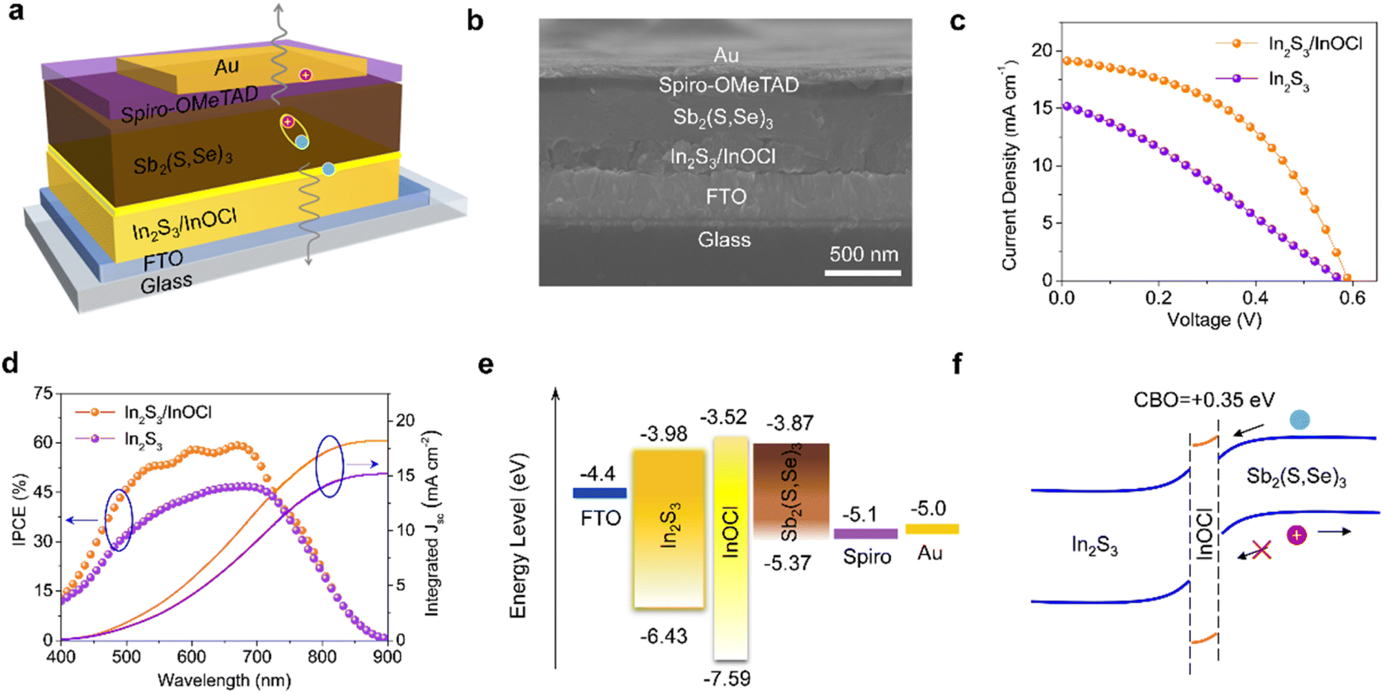 | ||
| Fig. 4 (a and b) The schematic illustration and cross-sectional SEM image of a complete device with the configuration of FTO/In2S3/InOCl/Sb2(S,Se)3/spiro-OMeTAD/Au, (c) J–V and (d) IPCE curves of the best-performing devices based on In2S3 and In2S3/InOCl buffer layers, (e) energy level diagrams of functional layers of Sb2(S,Se)3 solar cells, and (f) diagram of energy band alignments at the In2S3/InOCl/Sb2(S,Se)3 interface. | ||
| Devices | V oc (V) | J sc (mA cm−2) | FF (%) | η (%) | R s (Ω cm2) | R sh (Ω cm2) |
|---|---|---|---|---|---|---|
| In2S3 | 0.58 | 15.29 | 29.71 | 2.62 | 31.63 | 80.09 |
| In2S3/InOCl | 0.59 | 19.13 | 46.09 | 5.20 | 9.24 | 171.00 |
Fig. 4e summarizes energy level diagrams of functional layers of Sb2(S,Se)3 solar cells. The band structures of InOCl are obtained from UPS measurements (Fig. S14, ESI†), combined with an optical band gap of 4.07 eV from our calculations (Fig. S15, ESI†), and this value is consistent with previous experimental results.49 The band structures of In2S3 and Sb2(S,Se)3 layers are compiled from the literature.10,20 The positions of the conduction band minimum (CBM) and valence band maximum (VBM) of InOCl are estimated to be −3.52 and −7.59 eV. Herein a band gap of 4.07 eV is used for InOCl based on our calculations. As reflected by the level alignment at the In2S3/InOCl/Sb2(S,Se)3 interface according to Anderson's rule, the insertion of an InOCl interlayer would have two benefits. On one hand, the conduction band offset (CBO) of the InOCl/Sb2(S,Se)3 heterojunction is calculated to be +0.35 eV (−ΔEC). That is, a “spike” structure is formed at the In2S3/InOCl/Sb2(S,Se)3 interface as the CBM of InOCl is slightly higher than that of Sb2(S,Se)3 (Fig. 4f). It has been reported that, in contrast to the bandgap alignment of a “cliff” structure, a small “spike” of 0.1–0.4 eV is beneficial for the suppression of interfacial recombination.13,53 On the other hand, the deep VBM of InOCl is capable of effectively inhibiting the backflow of holes from the absorber layer to the buffer layer, which would also contribute to suppressed recombination of holes and electrons.13,54,55 Therefore, the incorporation of the InOCl interfacial layer affords superior band alignment for effective carrier transport.
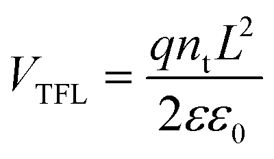
The InCl3 post-treatment might significantly change the electrical properties of In2S3-based buffer layers. The space-charge-limited current (SCLC) measurements were conducted to estimate the electron trap-state density of In2S3 buffer layers without and with the InCl3 post-treatment, as given in Fig. 5a and b. The electron-only single-carrier devices with the configuration FTO/ETL/PCBM/Au were constructed as shown in the inset. In the low applied voltage region, the I–V response involves a typical ohmic behavior (i.e., linear), implying an ideal interface capable of injecting sufficient charge from the electrodes to the semiconductor materials to allow SCLC with negligible trap states.56 With a further increase in bias voltage, the trap-filling limit (TFL) region characteristic of a sharp increase in voltage dependence is clearly observed as a result of full filling of trap states by injected carriers. Hence the onset voltage of the TFL (VTFL) is proportional to the density of trap states, which can be deduced from eqn (2):56
 | (2) |
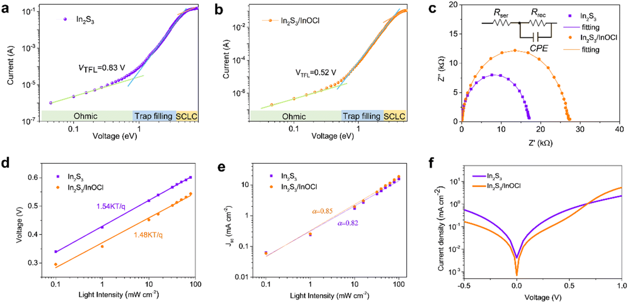 | ||
| Fig. 5 (a and b) The SCLC measurements of In2S3 and In2S3/InOCl-based electron-only single-carrier devices, and (c) the impedance spectroscopy spectra, (d) light intensity-dependent Voc measurements, (e) light intensity-dependent Jsc measurements, and (f) dark J–V curves of In2S3 and In2S3/InOCl-based Sb2(S,Se)3 solar cells. | ||
Impedance spectroscopy was conducted to explore the charge transfer and recombination processes in Sb2(S,Se)3 solar cells (Fig. 5c), on the basis of a simplified equivalent circuit model shown in the inset. Rser denotes the series internal resistance primarily derived from the resistance of the conductive electrode, and Rrec reflects the recombination resistance at the interfaces in solar cells. The nonideal capacitor of the CPE is defined using CPE-T and CPE-P which correspond to the interface capacitor and ideal capacitor, respectively.58 As shown, the Nyquist plots can be well fitted by using this model, and the fitting results are given in Table S2.† It is revealed that both cells share similar Rser values in view of the identical electrode employed in this work. The Rrec of the In2S3/InOCl-based device (27.28 kΩ) is much larger than that of the In2S3-based one (16.72 kΩ). The higher Rrec implies more effective inhibition of charge recombination in photovoltaic devices.56,58 This fact might be correlated with the effective healing of interface defects as a result of the incorporation of the InOCl interfacial layer, which benefits the efficient electron extraction at the ETL/absorber interface.
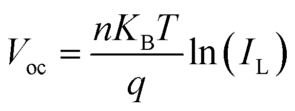
To further characterize the impacts of the InOCl interfacial layer on the charge transport and recombination processes in photovoltaic devices, light intensity-dependent Voc and Jsc measurements were performed for In2S3 and In2S3/InOCl-based Sb2(S,Se)3 solar cells and are shown in Fig. 5d and e. Under open-circuit circumstances, all photogenerated carriers are recombined as no charges are extracted from solar cells. The dependence of Voc and Jsc on the light intensity can be described by eqn (3) and (4):54,58
 | (3) |
| Jsc ∝ ILα | (4) |
The semi-logarithmic plots revealed that the estimated n of the In2S3/InOCl-based device is 1.48, smaller than that of 1.54 for the In2S3-based device, manifesting that the InOCl interfacial layer effectively suppresses the trap-assisted carrier recombination. The linear fitting reveals that the α values for In2S3 and In2S3/InOCl-based solar cells are estimated to be 0.82 and 0.85, respectively. The higher α (close to 1) indicates that the InOCl layer contributes to suppressed charge recombination and efficient charge collection.54 The J–V curves of both devices collected under dark conditions are shown in Fig. 5f. Both devices perform well as diodes, being capable of realizing good current rectification. Here we define the rectification ratio as Jv=0.5/Jv=−0.5, which are calculated to be 1.16 and 1.69 for In2S3 and In2S3/InOCl-based devices, respectively. A higher rectification ratio indicates a lower current leakage in the devices.58 That is, the presence of the InOCl layer significantly impedes the reverse saturation current in photovoltaic devices, favoring the enhancement of Jsc and FF.
3. Conclusions
In this work, a novel wide bandgap InOCl interfacial passivator was incorporated between the In2S3 buffer layer and absorber layer through InCl3 post-treatment for improved performance of Sb2(S,Se)3 solar cells. By referring to experimental and calculation investigations, we believe that the impacts of incorporating the InOCl layer are threefold: (1) the dominating one is the defect healing effect of the InOCl interfacial passivator to effectively suppress the formation of In vacancies and thus alleviate the recombination losses at the ETL/absorber interface; (2) the formation of a “spike” band structure at the ETL/absorber interface that suppresses the interface recombination and the deep VBM of wide-bandgap InOCl inhibits the backflow of holes from the absorber layer to the buffer layer; (3) the InOCl covering layer is capable of inhibiting the transformation of In2S3 into In(OH)3 in moist air. Benefitting from such positive effects of the incorporation of InOCl, a significantly improved PCE of 5.20% is obtained for Sb2(S,Se)3 solar cells, much higher than that of a pristine In2S3 based device (2.62%). This work develops a simple but effective pathway for the optimization of In2S3 ETLs for photovoltaic and other optoelectronic device applications.4. Experiments and calculations
4.1. Deposition of In2S3 buffer layers
The FTO (∼15 Ω sq−1) conducting glass was used as the substrate to deposit In2S3 buffer layers. Firstly, the substrates were thoroughly cleaned with detergent, deionized (DI) water, acetone, ethanol, and isopropanol, each for 20 min in sequence, under ultrasonic conditions, followed by drying with nitrogen (N2). Then the substrates underwent a typical UV/ozone treatment for 20 min. Secondly, In2S3 thin films were prepared by a conventional CBD method. Typically, 1.1059 g InCl3, 4.802 g citric acid, and 1.502 g thioacetamide (CH3CSNH2) were added into 200 mL DI water in sequence and stirred at room temperature until fully dissolved, obtaining the precursor solution for the deposition of In2S3 films. Then FTO substrates were vertically immersed into the precursor solution and kept at 70 °C for different durations under continuous stirring in a water bath kettle. The In2S3 film thickness could be facilely controlled by the CBD duration. The samples were taken out when the CBD processes were finished, followed by rinsing with DI water and ethanol, as well as drying with N2. Finally, the samples were annealed at 300 °C for 1.5 min on a hot plate in a N2 environment, obtaining In2S3 films for serving as the buffer layer of Sb2(S,Se)3 solar cells. As for the post-treatment of In2S3 films, 80 μL InCl3 methanol solution with different concentrations (0.01, 0.02, 0.04, and 0.08 g mL−1) was spin-coated on the FTO/In2S3 substrate, followed by sintering at 300 °C for 10 min in an ambient environment. This step produced the InOCl interface layer on the In2S3 buffer layer.4.2. Device fabrication
The Sb2(S,Se)3 absorber films were deposited onto the obtained In2S3 or In2S3/InOCl buffer layers by using the hydrothermal method, in which C4H4KO7Sb·0.5H2O, Na2S2O3·5H2O, and CH4N2Se were employed as Sb, S, and Se sources, respectively. Typically, 20 mM of C4H4KO7Sb·0.5H2O and 80 mM of Na2S2O3·5H2O diluted in 40 mL ultrapure water were added into a 50 mL Teflon tank, and 0.02 g of CH4N2Se was further added into the mixture solution under continuous stirring, obtaining a homogenous yellow solution. Then the buffer layer-coated FTO substrates were immersed in the solution mixture with the conducting side facing down inside the autoclave and tilted at an angle of about 75°. The autoclave was then sealed and kept at 135 °C for 110 minutes. When cooling down naturally, the substrates were taken out and rinsed with DI water and dried with a N2 flow. At last, the films were annealed at 350 °C for 10 min in a tube furnace under a N2 atmosphere. Furthermore, 1 mL chlorobenzene containing 36.6 mg spiro-OMeTAD, 14.5 μL tert-butylpyridine (TBP), and 9.5 μL of lithium bis(trifluoromethylsulfonyl)imide salt dissolved in acetonitrile (0.52 g mL−1) was dropped onto the Sb2(S,Se)3 film surface and spun with a speed rate of 3000 rpm for 30 s to deposit the HTL. Then, the HTL was annealed at 100 °C for 10 min on a hot plate. The superstrate Sb2(S,Se)3 solar cells were completed by thermal evaporation of Au as the metal electrode, and the active area of the devices was 0.06 cm2.4.3. Characterization
XRD spectra were collected on a diffractometer (X'Pert PRO MPD, Panalytical B. V, λ = 1.54056 Å). SEM images were obtained on a JEOL field emission scanning electron microscope (JSM-6700F). AFM images were collected on a Bruker atomic force microscope (Dimension). Absorption and transmission spectra were measured by using an Agilent spectrophotometer (CARY 5000). Raman spectroscopy was performed on a focal laser microRaman spectrometer (LabRam HR Evolution) by using a 532 nm laser as the excitation source. XPS was carried out on a Thermo Scientific K-Alpha spectrometer. UPS was conducted on a Thermo ESCALAB XI. The PCE of solar cells was achieved under the illumination of an Newport Oriel Sol 3A Solar Simulator (AM 1.5, 100 mW cm−2), coupled with a Keithley 2400 digital source meter. The IPCE spectra were collected on a QTest Station 1000 ADI system (Crowntech Inc.). Electrochemical impedance spectroscopy was performed under dark conditions with an applied voltage of 0.6 V by using a Zahner workstation (Zennium Pro), and the obtained data were fitted by using Z-view software.4.4. Calculations
The structural optimization of each structure is performed using the VASP, where an energy cutoff of 500 eV and the Perdew–Burke–Ernzerhof (PBE) functional within the generalized gradient approximation (GGA) are adopted. The lattice parameters and the coordinates of the atoms are fully relaxed, until the maximum force is less than 0.02 eV Å−1. For the surface systems, the structures are separated by a vacuum region of 16.0 Å in the Z direction, so that the interaction between the slab and its images arising from the periodic conditions can be ignored. When studying the adsorption of the InOCl monolayer on the β-In2S3 (110) surface, the van der Waals (vdW) interactions via the DFT-D2 method are used in order to properly describe the adsorption behaviors. In and S atoms in the bottom surface are saturated by using pseudo-hydrogen atoms to eliminate the effect of dangling bonds on the electronic structure. Charge transfer is obtained based on Bader analysis.Conflicts of interest
The authors declare no conflict of interest.Acknowledgements
C. W. and D. L. contributed equally to this work. The financial support from the Fundamental Research Funds for the Central Universities (No. PA2021KCPY0036), the National Natural Science Foundation of Anhui Province (No. 2108085ME147), the National Natural Science Foundation of Hefei City (No. 2022024), and the National Natural Science Foundation of China (No. U19A2089) is greatly acknowledged. R. Z. and C. W. conceived the idea. C. W., X. M., and R. Z designed and carried out the experiments and analyzed the data. C. W. carried out device optimizations. D. L. carried out the DFT calculations. L. W., Z. C., J. Z., and R. L. Z. H., assisted in experiments and data analysis. R. Z. and C. W. wrote the manuscript. All authors commented on the manuscript.References
- F. Fu, J. Li, T. C. Yang, H. Liang, A. Faes, Q. Jeangros, C. Ballif and Y. Hou, Adv. Mater., 2022, 34, e2106540 CrossRef PubMed.
- J. Liu, M. De Bastiani, E. Aydin, G. T. Harrison, Y. J. Gao, R. R. Pradhan, M. K. Eswaran, M. Mandal, W. B. Yan, A. Seitkhan, M. Babics, A. S. Subbiah, E. Ugur, F. Z. Xu, L. J. Xu, M. C. Wang, A. U. Rehman, A. Razzaq, J. X. Kang, R. Azmi, A. A. Said, F. H. Isikgor, T. G. Allen, D. Andrienko, U. Schwingenschlogl, F. Laquai and S. De Wolf, Science, 2022, 377, 302–306 CrossRef CAS PubMed.
- T. Walker, M. E. Stuckelberger, T. Nietzold, N. Mohan-Kumar, C. Ossig, M. Kahnt, F. Wittwer, B. Lai, D. Salomon, E. Colegrove and M. I. Bertoni, Nano Energy, 2022, 91, 106595 CrossRef CAS.
- J. Ramanujam, D. M. Bishop, T. K. Todorov, O. Gunawan, J. Rath, R. Nekovei, E. Artegiani and A. Romeo, Prog. Mater. Sci., 2020, 110, 100619 CrossRef CAS.
- S. Y. Wang, Y. Q. Zhao, B. Che, C. Li, X. L. Chen, R. F. Tang, J. B. Gong, X. M. Wang, G. L. Chen, T. Chen, J. M. Li and X. D. Xiao, Adv. Mater., 2022, 34, 2206242 CrossRef CAS PubMed.
- Z. T. Duan, X. Y. Liang, Y. Feng, H. Y. Ma, B. L. Liang, Y. Wang, S. P. Luo, S. F. Wang, R. E. I. Schropp, Y. H. Mai and Z. Q. Li, Adv. Mater., 2022, 34, 2202969 CrossRef CAS PubMed.
- Y. Q. Zhao, S. Y. Wang, C. H. Jiang, C. Li, P. Xiao, R. F. Tang, J. B. Gong, G. L. Chen, T. Chen, J. M. Li and X. D. Xiao, Adv. Energy Mater., 2022, 12, 2103015 CrossRef CAS.
- J. M. Li, Y. Q. Zhao, C. Li, S. Y. Wang, X. L. Chen, J. B. Gong, X. M. Wang and X. D. Xiao, Adv. Sci., 2022, 9, 2202356 CrossRef CAS PubMed.
- S. S. Shin, J. H. Suk, B. J. Kang, W. Yin, S. J. Lee, J. H. Noh, T. K. Ahn, F. Rotermund, I. S. Cho and S. I. Seok, Energy Environ. Sci., 2019, 12, 958–964 RSC.
- X. L. Mao, M. R. Bian, C. X. Wang, R. Zhou, L. Wan, Z. B. Zhang, J. Zhu, W. C. Chen, C. W. Shi and B. M. Xu, ACS Appl. Energy Mater., 2022, 5, 3022–3033 CrossRef CAS.
- X. Jin, Y. A. Fang, T. Salim, M. J. Feng, Z. T. Yuan, S. Hadke, T. C. Sum and L. H. Wong, Adv. Mater., 2021, 33, 2104346 CrossRef CAS PubMed.
- R. F. Tang, X. M. Wang, W. T. Lian, J. L. Huang, Q. Wei, M. L. Huang, Y. W. Yin, C. H. Jiang, S. F. Yang, G. C. Xing, S. Y. Chen, C. F. Zhu, X. J. Hao, M. A. Green and T. Chen, Nat. Energy, 2020, 5, 587–595 CrossRef CAS.
- H. L. Cai, R. Cao, J. X. Gao, C. Qian, B. Che, R. F. Tang, C. F. Zhu and T. Chen, Adv. Funct. Mater., 2022, 32, 2208243 CrossRef CAS.
- C. Qian, J. J. Li, K. W. Sun, C. H. Jiang, J. L. Huang, R. F. Tang, M. Green, B. Hoex, T. Chen and X. J. Hao, J. Mater. Chem. A, 2022, 10, 2835–2841 RSC.
- H. Deng, Y. Y. Zeng, M. Ishaq, S. J. Yuan, H. Zhang, X. K. Yang, M. M. Hou, U. Farooq, J. L. Huang, K. W. Sun, R. Webster, H. Wu, Z. H. Chen, F. Yi, H. S. Song, X. J. Hao and J. Tang, Adv. Funct. Mater., 2019, 29, 1901720 CrossRef.
- S. Y. Wang, Y. Q. Zhao, L. Q. Yao, C. Li, J. B. Gong, G. L. Chen, J. M. Li and X. D. Xiao, Sci. Bull., 2022, 67, 263–269 CrossRef CAS PubMed.
- J. H. Shi, Y. Q. Wang, M. R. Yang, Y. F. Gu, W. An, Y. Men, J. X. Yang and Y. C. Rui, Electrochim. Acta, 2021, 376, 138031 CrossRef CAS.
- M. A. Mughal, R. Engelken and R. Sharma, Sol Energy, 2015, 120, 131–146 CrossRef CAS.
- B. Yang, M. Wang, X. F. Hu, T. W. Zhou and Z. G. Zang, Nano Energy, 2019, 57, 718–727 CrossRef CAS.
- Y. Hou, X. Chen, S. Yang, Y. L. Zhong, C. Z. Li, H. J. Zhao and H. G. Yang, Nano Energy, 2017, 36, 102–109 CrossRef CAS.
- B. R. Lee and H. W. Jang, Electron. Mater. Lett., 2021, 17, 119–135 CrossRef CAS.
- J. L. Chen, W. Qiu, C. Y. Huang, L. Wu, C. Liu, Q. Q. Tian, Z. Y. Peng and J. Chen, Energy Technol., 2022, 10, 2200054 CrossRef CAS.
- X. Cui, C. W. Shi, C. Ying, Q. Wang, X. Sun and W. C. Chen, Mater. Sci. Semicond. Process., 2022, 137, 106186 CrossRef CAS.
- A. M. Huerta-Flores, N. A. Garcia-Gomez, S. M. de la Parra-Arciniega and E. M. Sanchez, Semicond. Sci. Technol., 2016, 31, 085011 CrossRef PubMed.
- T. Liu, X. Y. Liang, Y. F. Liu, X. L. Li, S. F. Wang, Y. H. Mai and Z. Q. Li, Adv. Sci., 2021, 8, 2100868 CrossRef CAS PubMed.
- C. Wang, S. C. Lu, S. Li, S. Y. Wang, X. T. Lin, J. Zhang, R. Kondrotas, K. H. Li, C. Chen and J. Tang, Nano Energy, 2020, 71, 104577 CrossRef CAS.
- B. Ma, M. F. Yue, P. Zhang, S. Z. Li, R. H. Cong, W. L. Gao and T. Yang, Catal. Commun., 2017, 88, 18–21 CrossRef CAS.
- F. Horani and E. Lifshitz, Chem. Mater., 2019, 31, 1784–1793 CrossRef CAS.
- E. Ghorbani and K. Albe, J. Appl. Phys., 2018, 123, 103103 CrossRef.
- W. J. Huang, L. Gan, H. T. Yang, N. Zhou, R. Y. Wang, W. H. Wu, H. Q. Li, Y. Ma, H. B. Zeng and T. Y. Zhai, Adv. Funct. Mater., 2017, 27, 1702448 CrossRef.
- Y. Zhao, D. Z. Yu, J. T. Lu, L. Tao, Z. F. Chen, Y. B. Yang, A. X. Wei, L. L. Tao, J. Liu, Z. Q. Zheng, M. M. Hao and J. B. Xu, Adv. Opt. Mater., 2019, 7, 1901085 CrossRef CAS.
- S. Yang, S. S. Chen, E. Mosconi, Y. J. Fang, X. Xiao, C. C. Wang, Y. Zhou, Z. H. Yu, J. J. Zhao, Y. L. Gao, F. De Angelis and J. S. Huang, Science, 2019, 365, 473–478 CrossRef CAS PubMed.
- T. Mueller, S. Schwertheim and W. R. Fahmer, PVSC: 2008 33rd IEEE Photovoltaic Specialists Conference, 2008, vol. 1–4, pp. 1785–1790 Search PubMed.
- M. M. Lee, J. Teuscher, T. Miyasaka, T. N. Murakami and H. J. Snaith, Science, 2012, 338, 643–647 CrossRef CAS PubMed.
- M. Dan, Q. Zhang, S. Yu, A. Prakash, Y. H. Lin and Y. Zhou, Appl. Catal., B, 2017, 217, 530–539 CrossRef CAS.
- L. X. Meng, Z. R. Yao, L. Cai, W. X. Wang, L. K. Zhang, K. F. Qiu, W. J. Lin, H. Shen and Z. C. Liang, Sol. Energy, 2020, 211, 759–766 CrossRef CAS.
- A. Omelianovych, J. H. Kim, L. Liudmila and B. T. Ahn, Curr. Appl. Phys., 2015, 15, 1641–1649 CrossRef.
- P. M. Sommeling, B. C. O'Regan, R. R. Haswell, H. J. P. Smit, N. J. Bakker, J. J. T. Smits, J. M. Kroon and J. A. M. van Roosmalen, J. Phys. Chem. B, 2006, 110, 19191–19197 CrossRef CAS PubMed.
- E. Karber, K. Otto, A. Katerski, A. Mere and M. Krunks, Mater. Sci. Semicond. Process., 2014, 25, 137–142 CrossRef CAS.
- Q. Gao, C. Cao, J. P. Ao, J. L. Bi, L. Y. Yao, J. J. Guo, G. Z. Sun, W. Liu, Y. Zhang, F. F. Liu and W. Li, Appl. Surf. Sci., 2022, 578, 152063 CrossRef CAS.
- M. G. Sandoval-Paz, M. Sotelo-Lerma, J. J. Valenzuela-Jauregui, M. Flores-Acosta and R. Ramirez-Bon, Thin Solid Films, 2005, 472, 5–10 CrossRef CAS.
- C. D. Lokhande, A. Ennaoui, P. S. Patil, M. Giersig, K. Diesner, M. Muller and H. Tributsch, Thin Solid Films, 1999, 340, 18–23 CrossRef CAS.
- W. Tian, C. Chen, L. X. Meng, W. W. Xu, F. R. Cao and L. Li, Adv. Energy Mater., 2020, 10, 1903951 CrossRef CAS.
- Y. T. Huang, S. R. Kavanagh, M. Righetto, M. Rusu, I. Levine, T. Unold, S. J. Zelewski, A. J. Sneyd, K. Zhang, L. Dai, A. J. Britton, J. Ye, J. Julin, M. Napari, Z. Zhang, J. Xiao, M. Laitinen, L. Torrente-Murciano, S. D. Stranks, A. Rao, L. M. Herz, D. O. Scanlon, A. Walsh and R. L. Z. Hoye, Nat. Commun., 2022, 13, 4960 CrossRef CAS PubMed.
- L. X. Meng, M. Wang, H. X. Sun, W. Tian, C. H. Xiao, S. L. Wu, F. R. Cao and L. Li, Adv. Mater., 2020, 32, 2002893 CrossRef CAS PubMed.
- H. Q. Yang, H. Zhao, H. X. Dong, W. Y. Yang and D. C. Chen, Mater. Res. Bull., 2009, 44, 1148–1153 CrossRef CAS.
- C. Karakaya, S. Ricote, D. Albin, E. Sanchez-Cortezon, B. Linares-Zea and R. J. Kee, Thermochim. Acta, 2015, 622, 55–63 CrossRef CAS.
- X. L. Xu, Y. D. Ma, B. B. Huang and Y. Dai, Phys. Chem. Chem. Phys., 2019, 21, 7440–7446 RSC.
- Q. Liang, H. Zhao, L. C. Ning, J. L. Wang, C. J. Zhang, L. Wang, A. H. Wei, Q. Zhao, H. Q. Yang and S. Z. Liu, Appl. Catal., B, 2014, 152, 390–396 CrossRef.
- M. Ishaq, H. Deng, S. Yuan, H. Zhang, J. Khan, U. Farooq, H. Song and J. Tang, Sol. RRL, 2018, 2, 1800144 CrossRef.
- C. H. Jiang, J. Zhou, R. F. Tang, W. T. Lian, X. M. Wang, X. Y. Lei, H. L. Zeng, C. F. Zhu, W. H. Tang and T. Chen, Energy Environ. Sci., 2021, 14, 359–364 RSC.
- L. Q. Yao, L. M. Lin, H. Liu, F. Y. Wu, J. M. Li, S. Y. Chen, Z. G. Huang and G. L. Chen, J. Mater. Sci. Technol., 2020, 58, 130–137 CrossRef CAS.
- C. Ding, Y. H. Zhang, F. Liu, Y. Kitabatake, S. Hayase, T. Toyoda, K. Yoshino, T. Minemoto, K. Katayama and Q. Shen, Nano Energy, 2018, 53, 17–26 CrossRef CAS.
- J. T. Zhou, R. Zhou, J. Zhu, P. Jiang, L. Wan, H. H. Niu, L. H. Hu, X. Yang, J. Z. Xu and B. M. Xu, Sol. RRL, 2021, 5, 2100494 CrossRef.
- J. T. Zhou, M. Lyu, J. Zhu, G. N. Li, Y. T. Li, S. Z. Jin, J. L. Song, H. H. Niu, J. Z. Xu and R. Zhou, ACS Appl. Energy Mater., 2022, 5, 3052–3063 CrossRef CAS.
- J. Han, X. Y. Pu, H. Zhou, Q. Cao, S. J. Wang, Z. W. He, B. Y. Gao, T. T. Li, J. S. Zhao and X. H. Li, ACS Appl. Mater. Interfaces, 2020, 12, 44297–44306 CrossRef CAS PubMed.
- L. G. Wang, L. Xia, Y. J. Wu and Y. Tian, ACS Sustainable Chem. Eng., 2016, 4, 2606–2614 CrossRef CAS.
- J. T. Zhou, X. T. Wei, J. Zhu, X. Yang, H. H. Niu, L. Wan, P. Jiang, J. Z. Xu, R. Zhou and G. Z. Cao, Sci. China Mater., 2020, 63, 1151–1162 CrossRef CAS.
Footnote |
| † Electronic supplementary information (ESI) available. See DOI: https://doi.org/10.1039/d3ta01736b |
| This journal is © The Royal Society of Chemistry 2023 |