DOI:
10.1039/D3NR01910A
(Communication)
Nanoscale, 2023,
15, 17326-17334
Synthesis of multiphase MoS2 heterostructures using temperature-controlled plasma-sulfurization for photodetector applications†
Received
25th April 2023
, Accepted 3rd October 2023
First published on 7th October 2023
Abstract
Two-dimensional (2D) materials exhibit outstanding performance in photodetectors because of their excellent optical and electronic properties. Specifically, 2D-MoS2, a transition metal dichalcogenide, is a prominent candidate for flexible and portable photodetectors based on its inherent phase-dependent tunable optical band gap properties. This research focused on creating high-performance photodetectors by carefully arranging out-of-plane 2D heterostructures. The process involved stacking different phases of MoS2 (1T and 2H) using controlled temperature during plasma-enhanced chemical vapor deposition. Among the various phase combinations, the best photocurrent response was obtained for the 1T/2H-MoS2 heterostructure, which exhibited an approximately two-fold higher photocurrent than the 2H/1T-MoS2 heterostructure and 2H/2H-MoS2 monostructure. The 1T/2H-MoS2 heterostructure exhibited a higher photoresponse than the monostructured MoS2 of the same thickness (1T/1T- and 2H/2H-MoS2, respectively). The effect of the stacking sequences of different phases was examined, and their photoperformances were investigated. This study demonstrates that phase engineering in 2D-MoS2 van der Waals heterostructures has significant potential for developing high-performance photodetectors.
1. Introduction
Two-dimensional (2D) layered nanomaterials, including graphene and transition metal dichalcogenides, are exemplary materials with exciting properties owing to their chemical composition, size, and atomic arrangement.1,2 Two-dimensional MoS2 has been intensively studied owing to its diverse phases and phase-dependent properties.3,4 MoS2 exhibits two principal phases with an arrangement of S atoms relative to Mo atoms, eliciting distinct symmetries of the 2H (trigonal prismatic) stable semiconducting phase and the 1T (octahedral) metastable metallic phase.5 Moreover, multilayered MoS2 exhibits covalent bonding between S and Mo atoms and weak van der Waals (vdW) interactions between the layers.6 In particular, 1T-MoS2 is unstable without additional electron injection into the S–Mo–S framework as it tends to aggregate because of the S–S vdW interactions and subsequently transforms into the more stable 2H-MoS2.7,8 Owing to these unique combinations of atoms and vdW interactions between the layers, MoS2 encompasses heterostructures and various crystalline phases.9 Additionally, the electronic band gap and band properties are phase- and layer-dependent. The band gap of MoS2 changes from indirect to direct as the number of layers decreases to that of a single layer.10 The photoluminescence of MoS2 disappears with an increasing number of layers.11 The semiconducting phase of MoS2 can absorb and generate electrons, whereas the metallic phase of MoS2 can transport and tunnel electrons through the layers. Therefore, the phases and stacking formations in heterostructures have been extensively used for applications of MoS2 in fields such as optoelectronics and photonics.12,13 Mechanical stacking is widely used to create high-quality heterostructures. However, controlling the area of the deposited material using this method is challenging.14 To circumvent this limitation, chemical vapor deposition (CVD) is preferred for producing heterostructures with high crystallization, large-area production, and sharp grain boundaries.15 Moreover, CVD requires high processing temperatures and multiple precursors for MoS2 synthesis.16 Multiphase stacking of a single material is very challenging in CVD and is yet to be reported. In addition to CVD, mechanical exfoliation,17 molecular beam epitaxy,18 and solution-based methods are common techniques for producing vdW heterostructures.19 However, these methods have challenges such as controlling the number of layers, the growth area, and complex processing steps.20 In contrast, plasma-enhanced CVD (PECVD) enables the synthesis of 2D materials at low temperatures using easy processing steps.21 Unlike the heterostructures of MoS2 stacked with different 2D materials, in this study, heterostructures were synthesized by stacking two different phases, namely, 1T and 2H, of MoS2 on top of each other using the PECVD method via a two-step synthesis. The 1T and 2H phases were controlled by varying the PECVD temperatures. Additionally, the photocurrent and photoswitching performances of devices prepared using different phases of MoS2 in the heterostructure materials were analyzed. The effects of the phases on the photocurrent results are discussed, along with a possible mechanism for photoperformance.
2. Experimental
1T/2H-MoS2 heterostructure synthesis
Table S1† lists the synthesis conditions for 1T- and 2H-MoS2 using plasma processing. Molybdenum (3 mm diameter × 3 mm thick pellet; 99.95%) was deposited on a Si substrate using e-beam evaporation at a deposition rate of 0.1 Å s−1. Molybdenum was sulfurized using PECVD in a 13.56 MHz inductively coupled plasma (ICP) chamber. To remove the unwanted particles and residues from the Mo metal surface, 20 sccm of Ar gas was used for 10 min before starting the experiment. Subsequently, 20 sccm of H2 gas was introduced into the metal chamber for 15 min to remove the natural oxide from the Mo metal (chamber pressure = 200 mTorr; radio frequency (RF) power = 200 W). The Ar cleaning conditions were used to heat the PECVD chamber to 150 or 300 °C. Sulfurization was subsequently performed in a 10![[thin space (1/6-em)]](https://www.rsc.org/images/entities/char_2009.gif) :10 sccm H2S:Ar plasma atmosphere for 1.5 h at 150 or 300 °C to achieve 1T- or 2H-MoS2, respectively. Our previous study demonstrated that the MoS2 crystallization changes with the processing temperature.22 Therefore, two different temperatures (150 and 300 °C) were used to obtain the 1T and 2H phases. Additionally, Mo deposition and sulfurization were repeated under the same conditions to produce secondary 1T- or 2H-MoS2 on the underlying MoS2 to obtain 1T/1T- (1T top on 1T bottom material), 2H/2H- (2H top on 2H bottom material) MoS2 monostructures, and 2H/1T- (2H top on 1T bottom material), and 1T/2H- (1T top on 2H bottom material) MoS2 heterostructures.
:10 sccm H2S:Ar plasma atmosphere for 1.5 h at 150 or 300 °C to achieve 1T- or 2H-MoS2, respectively. Our previous study demonstrated that the MoS2 crystallization changes with the processing temperature.22 Therefore, two different temperatures (150 and 300 °C) were used to obtain the 1T and 2H phases. Additionally, Mo deposition and sulfurization were repeated under the same conditions to produce secondary 1T- or 2H-MoS2 on the underlying MoS2 to obtain 1T/1T- (1T top on 1T bottom material), 2H/2H- (2H top on 2H bottom material) MoS2 monostructures, and 2H/1T- (2H top on 1T bottom material), and 1T/2H- (1T top on 2H bottom material) MoS2 heterostructures.
Characterization
The vibrational phonon modes were analyzed using Raman spectroscopy (Alpha300 M+, WITec GmbH, Germany) at a wavelength of 532 nm. X-ray photoelectron spectroscopy (XPS; XPS/AES/UPS, Thermo Scientific) was used to study the chemical composition and depth profiles of the materials. The interval time for each etching step during XPS profiling was 120 s. Homogeneous and continuous film formation was confirmed using optical microscopy (OM, Olympus, U-MSSP4). The thickness of 1T/2H-MoS2 was measured using atomic force microscopy (AFM, NX-100, Park System). High-resolution transmission electron microscopy (HRTEM, ARM 200F, JEOL) was used to characterize the top view of the 2D material. Furthermore, 1T/2H-MoS2 was etched using a focused ion beam (JIB-4601F, JEOL Ltd) for cross-sectional HRTEM analysis.
Device fabrication
The Au electrode was fabricated on a Si substrate using a shadow mask via e-beam deposition after hetero- and monostructural synthesis. A 20 nm-thick Ti layer was deposited as an adhesive layer. Subsequently, a 50 nm-thick Au layer was deposited onto the Ti/2D material structure.
Photocurrent measurements
A semiconductor characterization system (Keithley 4200-SCS) was used for electrical and photocurrent analyses at room temperature (∼22 °C) under ambient conditions. Fiber-coupled light-emitting diodes (Thorlabs, Inc.) were used for the photoresponse evaluation of different light sources with wavelengths of 420, 530, 660, and 1050 nm. An optical power meter (PM100D, Thorlabs, Inc.) with an S120VC sensor (±3%, Thorlabs, Inc.) was used to measure the power of the incident light.
3. Results and discussion
Scheme 1 shows the synthesis of the 1T/2H-MoS2 (1T/2H) vertical heterostructure using PECVD. Typically, the Mo metal precursor is deposited on the Si substrate, which undergoes further sulfurization in the PECVD chamber at 300 and 150 °C for the first and second steps, resulting in 2H-MoS2 and 1T-MoS2, respectively. A 1 nm-thick Mo-deposited Si substrate was loaded into the PECVD chamber for sulfurization under a 10:10 sccm H2:Ar plasma atmosphere. During the sulfurization process, the heating chuck was set to 150 °C to achieve 1T- and 300 °C to achieve 2H-MoS2. Once 1T- and 2H-MoS2 were synthesized as bottom materials on a separate substrate, a 1 nm-thick Mo layer was deposited on 1T- and 2H-MoS2. Subsequently, secondary sulfurization was performed to fabricate mono- and heterostructured MoS2 materials. Therefore, two monostructures, 1T/1T-MoS2 (1T/1T) and 2H/2H-MoS2 (2H/2H), and two heterostructures, 2H/1T-MoS2 (2H/1T) and 1T/2H-MoS2 (1T/2H), were produced.
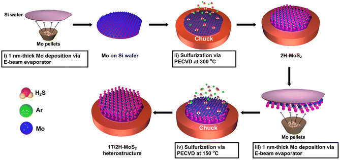 |
| | Scheme 1 Synthesis steps of the vertical stacking of 1T- and 2H-MoS2 on Si substrates using a 13.56 MHz ICP plasma process. | |
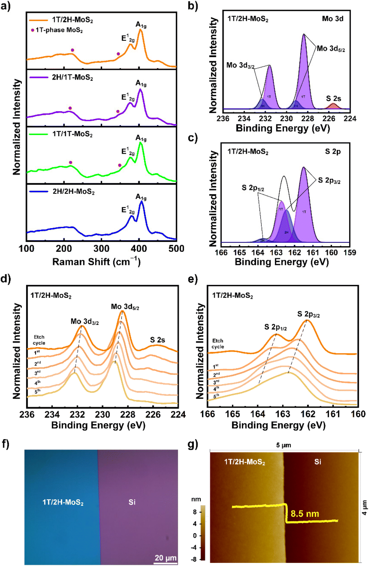
The individual phases of these heterostructures were further examined using Raman spectroscopy, as shown in Fig. 1a. The in-plane (E12g) and out-of-plane (A1g) resonance phonon modes of MoS2 occurred at 378 and 403 cm−1, respectively, for 1T/2H.23 The E12g and A1g peaks were associated with the 2H phase and were observed at 382 and 406 cm−1 for 2H/1T, 381 and 406 cm−1 for 1T/1T, and 382 and 406 cm−1 for 2H/2H. The characteristic peaks of the 1T phase were obtained for the 1T/2H, 2H/1T, and 1T/1T phases at 225 and 347 cm−1, corresponding to the J2 and J3 peaks, respectively.24 Negligible 1T characteristic peaks were observed in the 2H/2H Raman spectra because of S vacancies in the material structure. Furthermore, the presence of 2H peaks in the 1T/1T monostructure suggested that some metastable 1T phase was converted into the 2H phase in the prepared material.25,26 These Raman results confirmed the phase-selective synthesis of the 1T and 2H phases in the MoS2 mono/heterostructures using the PECVD method. XPS analyses were performed to examine the chemical composition of the synthesized mono/heterostructures, as shown in Fig. 1b and c. Fig. 1b shows the Mo core level peaks of the 1T/2H heterostructure, where the peaks at 228.6 eV (Mo 3d5/2) and 231.6 eV (Mo 3d3/2) represent the Mo4+ ion of 1T-MoS2,27 and those at 229.2 eV (Mo 3d5/2) and 232.6 eV (Mo 3d3/2) represent the Mo4+ ion of 2H-MoS2.28 A minor S 2s peak was also observed at 225.7 eV in the Mo 3d core peak spectra. The peaks at 161.5 and 162.7 eV correspond to S 2p3/2 and S 2p1/2 of 1T-MoS2, respectively, whereas the peaks at 162.4 and 163.7 eV correspond to the S 2p3/2 and S 2p1/2 of the S core level of 2H-MoS2, respectively (Fig. 1c).29,30 XPS analyses of the surface chemical compositions of 1T/1T, 2H/2H, and 2H/1T (Fig. S1a–f†) were performed, and similar observations were made for the 1T/2H heterostructure. To examine the interfacial structure of 1T/2H, XPS depth profiling was performed from the top (1T) to the bottom (2H) material. The Mo 3d core peak was recorded (Fig. 1d) as a function of the etching time. The binding energy increased when the film was etched with an Ar ion beam. This blue shift was attributed to a change in the chemical state of Mo4+ from the top to the bottom surface of the material, corresponding to a phase change from 1T to 2H in the 1T/2H structure. The S core-level-related S2− exhibited a decrease and broadening of the peaks as the etching progressed, owing to the damage caused by Ar etching, as shown in Fig. 1e. However, this peak was present until the fifth etching cycle, providing information on the MoS2 phases in the 1T/2H structure from the top to the bottom material. Furthermore, XPS depth profile analyses for the Mo 3d and S 2p of the 2H/1T heterostructure are shown in Fig. S2a and b,† respectively. From the beginning of the fourth cycle in the Mo 3d spectra of 2H/1T the Mo 3d peak shifted from a high binding energy to a low binding energy. This indicates that MoS2 is present in the 2H phase at the surface and in the 1T phase in the underlying material. The OM image shows the continuous and homogeneous formation of the 1T/2H film on the Si substrate (Fig. 1f). The 1T/2H thickness of the Si substrate, as measured using AFM, was approximately 8.5 nm (Fig. 1g). The thickness of the single-layer MoS2 was approximately 0.65 nm, resulting in approximately 13 layers of MoS2 in the 1T/2H structure.31
 |
| | Fig. 1 1T/2H-MoS2 characterization: (a) Raman spectroscopy and XPS surface analyses of (b) Mo 3d and (c) S 2p core peak spectra. XPS depth profile analyses of (d) Mo 3d and (e) S 2p core peak spectra. (f) OM and (g) AFM analyses of 1T/2H-MoS2 on Si wafer. | |
The HRTEM top-view image shown in Fig. 2a shows the edge-exposed 1T/2H surface. A selected-area electron diffraction (SAED) pattern is shown in the inset of Fig. 2a. Broad and hazy diffraction rings were observed in the SAED pattern owing to the nanocrystalline nature of the 1T/2H structure.32 The enlarged images of the green and violet regions in Fig. 2a reveal the triangular coordination of the 1T phase and the triangular prismatic coordination of the 2H phase on the surface.33Fig. 2b shows a cross-sectional HRTEM image of the 1T/2H material. Approximately 13 layers of MoS2 were observed, which is consistent with the AFM analysis. The lattice spacings of the 1T and 2H layers were determined from the profiles obtained along the red lines in the HRTEM cross-sectional images. The corresponding lattice spacing plots are shown in Fig. 2b. The surface HRTEM images of 1T/1T, 2H/2H, and 2H/1T are shown in Fig. S3a, b, and c,† respectively.
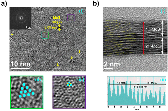 |
| | Fig. 2 (a) HRTEM top view and (b) HRTEM cross-sectional image of the 1T/2H-MoS2 vertical heterostructure. | |
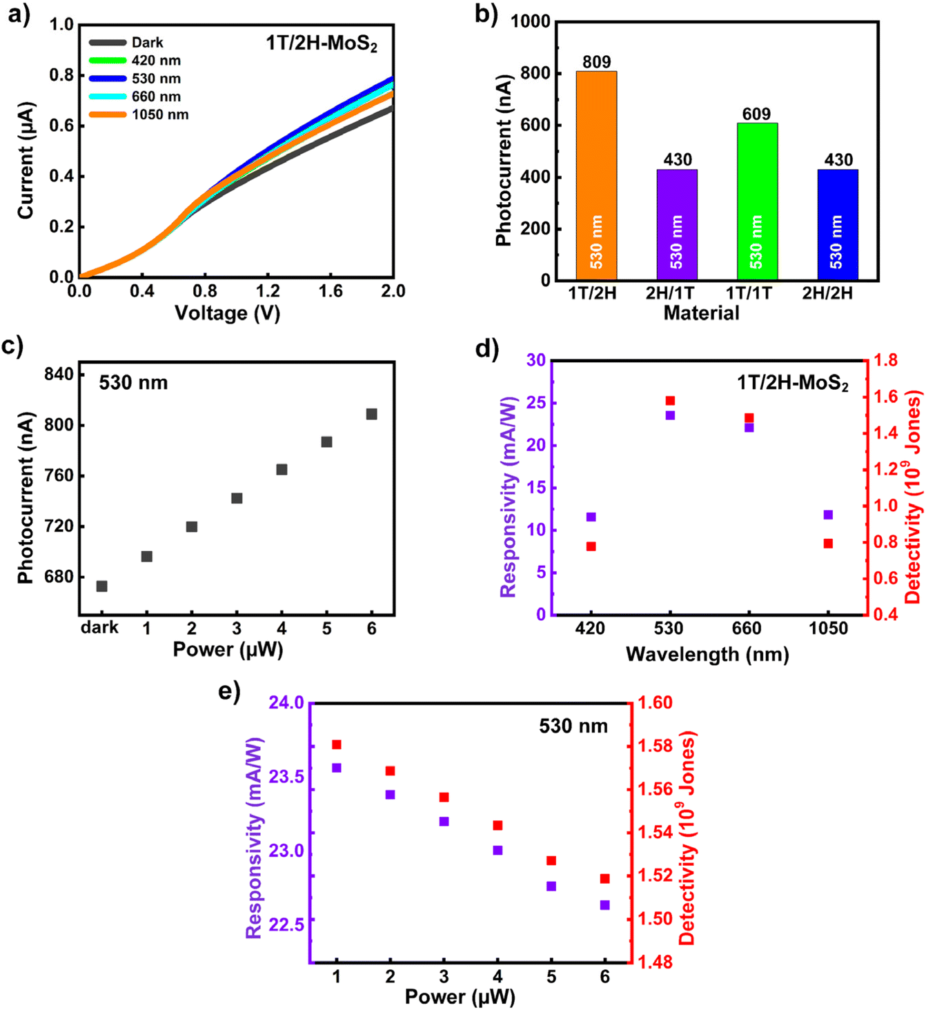
The photodetector performance of the prepared hetero- and monostructured materials was investigated using laser diode illumination and current measurements. Fig. 3a shows the photocurrent generation in the 1T/2H heterostructure under a positive bias at 420, 530, 660, and 1050 nm illumination wavelengths. The photocurrent curves for the 1T/1T, 2H/2H, and 2H/1T photodetectors at 420, 530, 660, and 1050 nm are plotted in Fig. S4a–c,† respectively. Among the wavelengths, 530 nm exhibited the best photocurrent generation for all prepared devices, except for the 1T/1T photodetector, which exhibited the highest photocurrent at 420 nm (Fig. 3a and Fig. S4a–c†). The photocurrent comparison of the prepared materials for the 530 nm illumination conditions at a power of 6 μW and 2 V bias is shown in Fig. 3b. The 2H/1T-MoS2 heterostructure and 2H/2H-MoS2 monostructure exhibited similar photocurrents of 430 nA, whereas 1T/1T and 1T/2H exhibited photocurrents of 609 and 809 nA, respectively, under the 530 nm illumination conditions at a of power 6 μW and a bias of 2 V. Additionally, the power vs. photocurrent graph was recorded under 530 nm illumination at a voltage bias of 2 V, as shown in Fig. 3c. The photocurrent exhibited a linear trend with an increasing illumination power. The photocurrent exhibited a similar trend at other wavelengths; however, the highest photocurrent was observed at 530 nm, as shown in Fig. 3a. The photoresponsivity and detectivity values of the 1T/2H photodetector at various wavelengths were plotted as shown in Fig. 3d. The 1T/2H photodetector exhibited better performance than the other photodetectors with higher responsivity and detectivity values when exposed to 530 nm irradiation. As seen in Fig. S4d and e,† the 1T/1T photoresponsivity and detectivity performance is better than that of the other photodetector materials (except 1T/2H-MoS2). Besides, 2H/2H and 2H/1T showed the same performance. Next, the typical responsivity and detectivity values corresponding to various power values for a 530 nm laser were calculated and are plotted in Fig. 3e. The responsivity and detectivity exhibit a linearly negative correlation with the applied illumination power, contrary to the photocurrent trend. The responsivity and detectivity demonstrate the photocurrent generation efficiency of the individual material. The responsivity and detectivity are directly proportional to the generated photocurrent and inversely proportional to the illumination power. This reduction in photoresponsivity and detectivity can be attributed to trap sites within the 1T/2H material, primarily at the interfaces and grain boundaries.34 These trap sites and interfaces impose a specific limit on generating electron–hole pairs upon illumination. With higher illumination power, the density of available states decreases, leading to the saturation of the photoresponse. As a result, the efficiency of photocurrent generation diminishes even as the illumination power increases. Hence, the trap sites in MoS2 arise due to the grain boundaries and the interfaces between the individual layers in the 1T/2H-MoS2 heterostructure, exhibiting negative responsivity and detectivity trends.35,36 The dependence of the responsivity and detectivity on the generated photocurrent can be understood using eqn (1) and (2):
| | | Iphoto = Iillumination − Idark | (2) |
where
R is the responsivity,
Iphoto is the photocurrent,
Plight is the power of the light,
Iillumination is the photocurrent under light conditions, and
Idark is the photocurrent under dark conditions. Detectivity is an essential criterion in the evolution of photodetectors. A higher detectivity indicates that the photodetector can detect even lower-intensity signals, suggesting that it competes with the noise of the detector.
Eqn (3) was used to calculate the detectivity.
where
A is the effective area of the detector, Δ
f is the frequency bandwidth, and
Inoise is the noise current. In photodetector applications,
Idark corresponds to
Inoise, and
Idark is independent of the frequency.
37 Therefore, the derived formula is as follows:
38| | | D* = R(A)1/2/(2eIdark)1/2. | (4) |
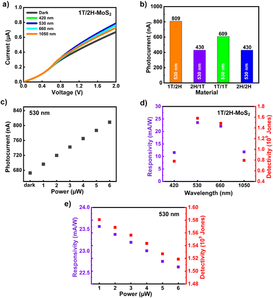 |
| | Fig. 3 (a) Current–voltage output curves of the 1T/2H-MoS2/Si photodetector under illumination with various wavelengths. (b) Current–voltage comparison of the 1T/2H- and 2H/1T-MoS2 heterostructures and the 1T/1T- and 2H/2H monostructures under 6 μW of 530 nm light power. (c) Photocurrent vs. power of light analysis, (d) photoresponsivity and detectivity analysis of 1T/2H-MoS2 under 1 μW of 420, 530, 660, and 1050 nm, and (e) photoresponsivity and detectivity vs. power of light for a 530 nm laser as the best performance of 1T/2H-MoS2. | |
The highest photoresponsivity of the 1T/2H photodetector measured at 1 μW at 530 nm illumination under a 2 V bias was 23.6 mA W−1. The corresponding detectivity value was approximately 1.58 × 10⁹ Jones, implying the best performance among the reported MoS2 detectors. Table S2† compares the responsivity and detectivity of the 1T/2H photodetector with those reported in other studies. The 1T/2H heterostructure material exhibited a comparably high responsivity, good detectivity, and low decay time in the green colour range.
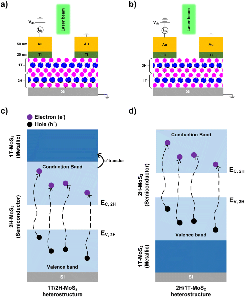
A mechanism is proposed to provide a better understanding of the photodetector performance of the 1T/2H heterostructure, as compared to the other prepared heterostructures and monostructures. The characterization and photodetector performance of the heterostructure showed that the interface formation between the 1T and 2H phases played a significant role in enhancing the photodetection performance. Scheme 2a and b show photodetector schematics illustrating the electrical connections under laser illumination with a constant drain–source voltage (Vds) for the 1T/2H and 2H/1T heterostructures, respectively. The mechanisms corresponding to these photodetectors are shown in Scheme 2c for 1T/2H and in Scheme 2d for 2H/1T. Valence band electrons are excited by photon energy and jump to the conduction band, leaving behind holes in the valence band. The excited electrons in the conduction band and leftover holes in the valence band are collectively called electron–hole pairs.39 Electron–hole pair generation after photon incidence in 2H-MoS2 is more efficient than that in 1T-MoS2, owing to the presence of a band gap and charge separation.40 The recombination of electron–hole pairs can occur because of defects or vacancies and insufficient pair separation in the structure. In the 1T/2H heterostructure, photons are separated in the bottom 2H-MoS2, and electrons are efficiently transmitted to the top 1T-MoS2 structure. Because of their 1T metallic behavior, electrons are quickly transported to the electrode with low resistance. Therefore, combining the 1T and 2H phases contributes to good performance by generating a high photocurrent in the 1T/2H heterostructure through the retention and generation of electron–hole pairs. The 1T/1T monostructure exhibited the second-best performance as it was structurally similar to the 1T/2H heterostructure. Because the 1T phase is unstable, some parts of the 1T phase are converted into the 2H phase in ambient air. Therefore, the presence of a lateral heterointerface between the 2H and 1T phases in the 1T/1T monostructure was assumed. The structural characterization of 1T/1T (Raman spectroscopy, XPS, and TEM) also confirmed the presence of the 2H phase. This heterointerface retains and generates electron–hole pairs similar to those described for the 2H/1T heterostructure. However, the efficiency of the electron–hole pair separation and vertical transport of electrons in the 1T/1T monostructure was lower than that in 1T/2H. Therefore, 1T/2H exhibited the best photoresponse. However, in the 2H/1T heterostructure, 2H-MoS2 contributed to the photocurrent generation, and the absence of an overall electron-trapping layer on top resulted in less photocurrent generation. Additionally, it is difficult for electrons in the bottom metallic 1T phase to transmit and recombine easily in the semiconductor phase. Consequently, the 2H/1T heterostructure exhibited the same current value as that of 2H/2H because only the 2H phase influenced the photocurrent in the 2H/1T heterostructure. Additionally, during the second step of the synthesis of the 2H/1T heterostructure, the initial bottom 1T MoS2 may convert into the 2H phase as the synthesis temperature reaches 300 °C, effectively synthesizing the 2H/2H phase in the 2H/1T heterostructure. Therefore, the 2H/2H and 2H/1T heterostructures exhibited similar performances. Overall, the band structure engineering of 1T/2H was better than that of 2H/1T, 1T/1T, and 2H/2H; therefore, it exhibited the best overall photoresponsivity and detectivity performance.
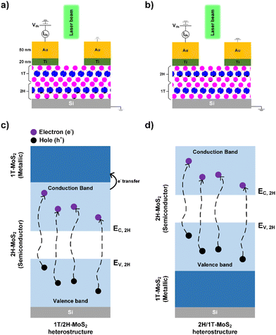 |
| | Scheme 2 Cross-sectional view of (a) 1T/2H-MoS2 and (b) 2H/1T-MoS2 photodetector structures. The corresponding electron–hole pair generation mechanism for (c) 1T/2H-MoS2 and (d) 2H/1T-MoS2. | |
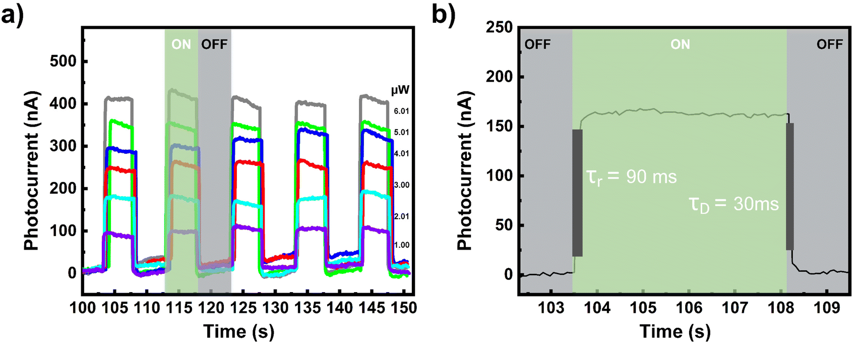
Finally, the photoswitching performance of the 1T/2H photodetector was investigated to determine its fast photoperformance. Fig. 4a shows the photoswitching currents (IDS) of the 1T/2H photodetector at different light powers. The rise (τr) and decay (τD) times correspond to the times required to increase the photocurrent from 10% to 90% of the maximum value and decrease the photocurrent from 90% to 10% of the maximum value, respectively. The rise time was determined to be 90 ms, whereas the decay time was determined to be 30 ms. In Fig. 4b the details of the rise and decay times for a single ON/OFF cycle of 1T/2H are provided. Table S2† also compares the photoswitching times of the 1T/2H heterostructure with those of other MoS2-based studies. Among the reported photodetectors, 1T/2H exhibits the best decay time.
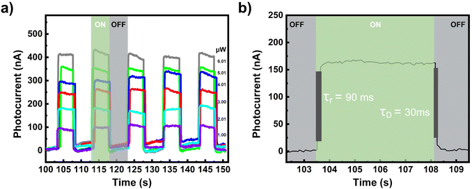 |
| | Fig. 4 (a) Photoswitching curves for different powers of the 530 nm laser and (b) the rise and decay times according to a single ON/OFF cycle of the 1T/2H-MoS2 photodetector. | |
4. Conclusions
The phase-dependent photoresponse study of MoS2 hetero and mono structures suggests that the vertically stacked 1T/2H-MoS2 has enhanced photoresponse due to the effective generation and separation of electron–hole pair upon illumination. The layered stacking in MoS2 showed the highest photocurrent for 530 nm illumination wavelength. The dependency of the photocurrent, photoresponsivity, and detectivity on the illumination power was observed and confirmed for all prepared materials. Furthermore, this study demonstrates the plasma-assisted and temperature-controlled synthesis of multiphase (1T and 2H) MoS2 stacked heterostructures and monostructures on a Si substrate and their photoresponse properties. Among the prepared materials, the photodetector device fabricated using 1T/2H-MoS2 exhibited the highest photoresponsivity of approximately 23.6 mA W−1, a photodetectivity of approximately 109 Jones, and a photoswitching time of 90 ms under 530 nm light irradiation. Furthermore, the 1T/2H-MoS2 photodetector exhibited a two-fold higher photocurrent response than the other photodetectors, with a photocurrent of 809 nA at 6 μW under 530 nm illumination at a 2 V bias. The prepared 1T/2H-MoS2 vdW heterostructure photodetector device exhibited the best performance because of the retention and generation of electron–hole pairs through phase engineering. The stacking sequence of the metallic and semiconducting MoS2 phases highlighted the functionality of the device. Therefore, the reported procedure is promising and versatile for synthesizing multiphase 2D optoelectronic devices.
Conflicts of interest
There are no conflicts to declare.
Acknowledgements
This research was supported by the Basic Science Research Program through the National Research Foundation of Korea (NRF), funded by the Ministry of Education (2022R1A3B1078163 and 2022R1A4A1031182) and has been conducted with the support of the Korea Institute of Industrial Technology as “Establishment of a Rapid Manufacturing Platform for Ceramic Additive Manufacturing (kitech EH-23-0002).”
References
- Y. Chen, Z. Fan, Z. Zhang, W. Niu, C. Li, N. Yang, B. Chen and H. Zhang, Chem. Rev., 2018, 118, 6409–6455 CrossRef CAS PubMed.
- X. Chen, R. Li, Y. Li, Y. Wang, F. Zhang and M. Zhang, Mater. Sci. Semicond. Process., 2022, 138, 106268 CrossRef CAS.
- X. Song, X. Liu, D. Yu, C. Huo, J. Ji, X. Li, S. Zhang, Y. Zou, G. Zhu, Y. Wang, M. Wu, A. Xie and H. Zeng, ACS Appl. Mater. Interfaces, 2018, 10, 2801–2809 CrossRef CAS PubMed.
- L. Wu, A. Longo, N. Y. Dzade, A. Sharma, M. M. R. M. Hendrix, A. A. Bol, N. H. de Leeuw, E. J. M. Hensen and J. P. Hofmann, ChemSusChem, 2019, 12, 4383–4389 CrossRef CAS PubMed.
- Y. Gao, S. Wang, B. Wang, Z. Jiang and T. Fang, Small, 2022, 18, 2202956 CrossRef CAS PubMed.
- X. Sun, B. Zhang, Y. Li, X. Luo, G. Li, Y. Chen, C. Zhang and J. He, ACS Nano, 2018, 12, 11376–11385 CrossRef CAS PubMed.
- Y. Zhang, Y. Kuwahara, K. Mori and H. Yamashita, Langmuir, 2020, 36, 1174–1182 CrossRef CAS PubMed.
- S. Deng, M. Luo, C. Ai, Y. Zhang, B. Liu, L. Huang, Z. Jiang, Q. Zhang, L. Gu, S. Lin, X. Wang, L. Yu, J. Wen, J. Wang, G. Pan, X. Xia and J. Tu, Angew. Chem., Int. Ed., 2019, 58, 16289–16296 CrossRef CAS PubMed.
- C. Sun, L. Wang, W. Zhao, L. Xie, J. Wang, J. Li, B. Li, S. Liu, Z. Zhuang and Q. Zhao, Adv. Funct. Mater., 2022, 32, 2206163 CrossRef CAS.
- B. Han and Y. H. Hu, Energy Sci. Eng., 2016, 4, 285–304 CrossRef CAS.
- A. Splendiani, L. Sun, Y. Zhang, T. Li, J. Kim, C. Y. Chim, G. Galli and F. Wang, Nano Lett., 2010, 10, 1271–1275 CrossRef CAS PubMed.
- A. A. A. Abdelazeez, A. B. G. Trabelsi, F. H. Alkallas and M. Rabia, Sol. Energy, 2022, 248, 251–259 CrossRef CAS.
- M. C. Sahu, S. Sahoo, S. K. Mallik, A. K. Jena and S. Sahoo, Adv. Mater. Technol., 2022, 8, 2201125 CrossRef.
- J. B. Lee, Y. R. Lim, A. K. Katiyar, W. Song, J. Lim, S. Bae, T. W. Kim, S. K. Lee and J. H. Ahn, Adv. Mater., 2019, 31, 1904194 CrossRef CAS PubMed.
- M. Diao, H. Li, R. Hou, Y. Liang, J. Wang, Z. Luo, Z. Huang and C. Zhang, ACS Appl. Mater. Interfaces, 2020, 12, 7423–7431 CrossRef CAS PubMed.
- X. Bai, S. Li, S. Das, L. Du, Y. Dai, L. Yao, R. Raju, M. Du, H. Lipsanen and Z. Sun, Nanoscale, 2021, 13, 4537–4542 RSC.
- C. Maestre, Y. Li, V. Garnier, P. Steyer, S. Roux, A. Plaud, A. Loiseau, J. Barjon, L. Ren, C. Robert, B. Han, X. Marie, C. Journet and B. Toury, 2D Mater., 2022, 9, 035008 CrossRef.
- P. Guha, J. Y. Park, J. Jo, Y. Chang, H. Bae, R. K. Saroj, H. Lee, M. Kim and G. C. Yi, 2D Mater., 2022, 9, 025006 CrossRef.
- J. B. Lee, Y. R. Lim, A. K. Katiyar, W. Song, J. Lim, S. Bae, T. W. Kim, S. K. Lee and J. H. Ahn, Adv. Mater., 2019, 31, 1904194 CrossRef CAS PubMed.
- X. Yu, X. Wang, F. Zhou, J. Qu and J. Song, Adv. Funct. Mater., 2021, 31, 2104260 CrossRef CAS.
- H.-U. Kim, V. Kanade, M. Kim, K. S. Kim, B. S. An, H. Seok, H. Yoo, L. E. Chaney, S. I. Kim, C. W. Yang, G. Y. Yeom, D. Whang, J. H. Lee and T. Kim, Wafer-Scale and Low-Temperature Growth of 1T-WS2 Film for Efficient and Stable Hydrogen Evolution Reaction, Small, 2020, 16(6), 2070033 CrossRef , DOI: https://doi.org/10.1002/smll.202070033.
- H.-U. Kim, M. Kim, H. Seok, K.-Y. Park, J.-Y. Moon, J. Park, B.-S. An, H. J. Jung, V. P. Dravid, D. Whang, J.-H. Lee and T. Kim, ChemSusChem, 2021, 14, 1344–1350 CrossRef CAS PubMed.
- H. Niu, Z. Zou, Q. Wang, K. Zhu, K. Ye, G. Wang, D. Cao and J. Yan, Chem. Eng. J., 2020, 399, 125672 CrossRef CAS.
- U. N. Pan, V. Sharma, T. Kshetri, T. I. Singh, D. R. Paudel, N. H. Kim and J. H. Lee, Small, 2020, 16, 2001691 CrossRef CAS PubMed.
- K. Le, X. Zhang, Q. Zhao, Y. Liu, P. Yi, S. Xu and W. Liu, ACS Appl. Mater. Interfaces, 2021, 13, 44427–44439 CrossRef CAS PubMed.
- Y. Yao, K. Ao, P. Lv and Q. Wei, Nanomaterials, 2019, 9, 844 CrossRef CAS PubMed.
- M. Acerce, D. Voiry and M. Chhowalla, Nat. Nanotechnol., 2015, 10, 313–318 CrossRef CAS PubMed.
- X. Lin, D. Xue, L. Zhao, F. Zong, X. Duan, X. Pan, J. Zhang and Q. Li, Chem. Eng. J., 2019, 356, 483–491 CrossRef CAS.
- S. S. Singha, S. Rudra, S. Mondal, M. Pradhan, A. K. Nayak, B. Satpati, P. Pal, K. Das and A. Singha, Electrochim. Acta, 2020, 338, 135815 CrossRef CAS.
- E. Er, H.-L. Hou, A. Criado, J. Langer, M. Möller, N. Erk, L. M. Liz-Marzan and M. Prato, Chem. Mater., 2019, 31, 5725–5734 CrossRef CAS.
- X. Li and H. Zhu, J. Materiomics, 2015, 1, 33–44 CrossRef.
- X. Xu, Z. Wang, S. Lopatin, M. A. Quevedo-Lopez and H. N. Alshareef, 2D Mater., 2018, 6, 015030 CrossRef.
- H. Liu, R. Wu, H. Zhang and M. Ma, ChemCatChem, 2020, 12, 893–902 CrossRef CAS.
- O. Lopez-Sanchez, D. Lembke, M. Kayci, A. Radenovic and A. Kis, Nat. Nanotechnol., 2013, 8, 497–501 CrossRef CAS PubMed.
- S. Ghatak, A. N. Pal and A. Ghosh, ACS Nano, 2011, 5, 7707–7712 CrossRef CAS PubMed.
- X. Wang, P. Wang, J. Wang, W. Hu, X. Zhou, N. Guo, H. Huang, S. Sun, H. Shen, T. Lin, M. Tang, L. Liao, A. Jiang, J. Sun, X. Meng, X. Chen, W. Lu and J. Chu, Adv. Mater., 2015, 27, 6575–6581 CrossRef CAS PubMed.
- C. H. Ji, K. T. Kim and S. Y. Oh, RSC Adv., 2018, 8, 8302–8309 RSC.
- C. K. Kanade, H. Seok, V. K. Kanade, K. Aydin, H.-U. Kim, S. B. Mitta, W. J. Yoo and T. Kim, ACS Appl. Mater. Interfaces, 2021, 13, 8710–8717 CrossRef CAS PubMed.
- Electron–hole pair in semiconductors, https://www.nuclear-power.com/nuclear-engineering/radiation-detection/semiconductor-detectors/what-are-semiconductors-properties-of-semiconductors/electron-hole-pair/, accessed: February, 2023.
- M. Zheng, S. Lin, L. Xu, L. Zhu and Z. L. Wang, Adv. Mater., 2020, 32, 2000928 CrossRef CAS PubMed.
|
| This journal is © The Royal Society of Chemistry 2023 |
Click here to see how this site uses Cookies. View our privacy policy here. 
 ab,
Chaitanya
Kanade‡
ab,
Chaitanya
Kanade‡