
 Open Access Article
 This Open Access Article is licensed under a
 Creative Commons Attribution 3.0 Unported Licence
Integrated 4-terminal single-contact nanoelectromechanical relays implemented in a silicon-on-insulator foundry process†
Yingying
Li
 a,
Elliott
Worsey
b,
Simon J.
Bleiker
a,
Pierre
Edinger
a,
Mukesh Kumar
Kulsreshath
b,
Qi
Tang
b,
Alain Yuji
Takabayashi
c,
Niels
Quack‡
c,
Peter
Verheyen
d,
Wim
Bogaerts
de,
Kristinn B.
Gylfason
a,
Dinesh
Pamunuwa
b and
Frank
Niklaus
*a
a,
Elliott
Worsey
b,
Simon J.
Bleiker
a,
Pierre
Edinger
a,
Mukesh Kumar
Kulsreshath
b,
Qi
Tang
b,
Alain Yuji
Takabayashi
c,
Niels
Quack‡
c,
Peter
Verheyen
d,
Wim
Bogaerts
de,
Kristinn B.
Gylfason
a,
Dinesh
Pamunuwa
b and
Frank
Niklaus
*a
aKTH Royal Institute of Technology, 11428 Stockholm, Sweden. E-mail: frank@kth.se
bUniversity of Bristol, BS8 1UB Bristol, UK
cÉcole Polytechnique Fédérale de Lausanne (EPFL), 1015 Lausanne, Switzerland
dIMEC, 3001 Leuven, Belgium
eGhent University, 9052 Gent, Belgium
First published on 13th October 2023
Abstract
Integrated nanoelectromechanical (NEM) relays can be used instead of transistors to implement ultra-low power logic circuits, due to their abrupt turn off characteristics and zero off-state leakage. Further, realizing circuits with 4-terminal (4-T) NEM relays enables significant reduction in circuit device count compared to conventional transistor circuits. For practical 4-T NEM circuits, however, the relays need to be miniaturized and integrated with high-density back-end-of-line (BEOL) interconnects, which is challenging and has not been realized to date. Here, we present electrostatically actuated silicon 4-T NEM relays that are integrated with multi-layer BEOL metal interconnects, implemented using a commercial silicon-on-insulator (SOI) foundry process. We demonstrate 4-T switching and the use of body-biasing to reduce pull-in voltage of a relay with a 300 nm airgap, from 15.8 V to 7.8 V, consistent with predictions of the finite-element model. Our 4-T NEM relay technology enables new possibilities for realizing NEM-based circuits for applications demanding harsh environment computation and zero standby power, in industries such as automotive, Internet-of-Things, and aerospace.
Nanoelectromechanical (NEM) relays have attracted considerable interest due to their inherent characteristics such as zero off-state leakage, steep switching transition, and harsh-environment operation capabilities, which make them ideally suited as digital switches for ultra-low power computation.1–5 4-Terminal (4-T) NEM relays decouple the signal path across the relay from the on/off actuation control such that the pull-in behaviour is determined by the voltage difference between the gate and body terminals, regardless of the signal voltage.6 This feature distinguishes 4-T relays from both CMOS transistors and conventional 3-terminal (3-T) NEM relays that share a common source electrode between the two electrical paths.7,8 In this way, the 4-T relay design enables logic circuits to be constructed with far fewer devices compared to transistor-based and 3-T NEM relay-based logic circuits.9 Also, the decoupling of the actuation and signal voltages allows the pull-in voltage of 4-T NEM relays to be reduced by employing body-biasing, where the beam or gate has a static voltage bias applied to reduce the voltage swing required for actuation. Although basic NEM relay-based logic functions were introduced over a decade ago,10–13 reliable miniaturization and integration methods for making NEM relay-based integrated circuits with multi-layer metal interconnect stacks have not been demonstrated. While several 4-T relays have been reported to date,6–9,14,15 as summarized in Table S1,† these are not integrated,15 and moreover have either a large footprint6–9,14 or a high pull-in voltage.6,7,9 Generally, small relay footprints are desirable to reduce cost, while the energy consumption of 4-T relays reduces inversely with the square of the voltage swing.
To demonstrate that these issues can be overcome, we report for the first time, nanoscale, silicon (Si) 4-T NEM relays that are patterned in front-end-of-line (FEOL) processing and monolithically integrated with back-end-of-line (BEOL) metallic interconnect layers manufactured in a commercial silicon-on-insulator (SOI) foundry platform (iSiPP50G by IMEC16–19). The foundry wafers containing the NEM relay structures and interconnects are post-processed to implement the electrical isolation between the control and signal paths of the 4-T NEM relays, the metallization of the contacts of the 4-T NEM relays, and the suspension of the movable sections of the relays. These post-processing steps are fully foundry compatible and can in principle be included into the commercial foundry process flow. This compatibility is critical to lower the threshold for potential commercial use and opens entirely new possibilities for efficient manufacturing of very-large-scale integrated (VLSI) NEM relay-based logic circuits at high yield.
The concept of our integrated Si 4-T NEM relay is illustrated in Fig. 1a; the relay is structured on the Si device layer with surrounding metal interconnect routings and is suspended within a cavity that is created at the end of the BEOL fabrication by post-processing of the foundry wafers. This integration method enables seamless incorporation of Si NEM relays in an existing foundry platform, without the need for intricate 3D stacking or wafer bonding processes. The relay consists of four terminals: two movable beams, connected to the source (S) and the body (B) terminals, as well as fixed drain (D) and gate (G) terminals. Each terminal of the relay passes through the cavity side walls and is electrically connected to an aluminium (Al) contact pad on the chip surface through several metallization routing layers embedded in the BEOL stack. The dielectric plug (aluminium oxide, AlOx, shown in green in Fig. 1a and b) mechanically connects the two beams but electrically isolates the body and source terminals. The 4-T NEM relay is actuated by applying a voltage between the gate and body terminals, thereby inducing electrostatic attraction between them, and deflecting the mechanically connected beams of the body and source terminals to establish an electrical contact between the source and the drain terminals. A 4-T relay with a similar architecture was demonstrated by Reynolds et al.,9 but their focus was on proof-of-concept of the relay principle and the resulting circuit efficiencies using larger microscale relay prototypes fabricated on an SOI wafer. Recently, we presented the fabrication of a 4-T NEM relay in the Si device layer of SOI substrate without metal interconnects.15 In contrast, in this work we demonstrate the first nanoscale 4-T NEM relay integrated with multi-layer metal interconnects, featuring a ∼10× reduction in critical dimension compared to the relays presented in ref. 9 (from 2 μm down to 200 nm). These advancements in integration and miniaturization are pivotal for the development of large-scale integrated NEM relay-based circuits. To demonstrate the viability of our 4-T NEM relays with integrated metal interconnects, we manufactured and characterized six integrated Si 4-T NEM relays with Au contacts deposited by physical vapor deposition (PVD) (see Fig. 1b for an example). We investigated the actuation behaviour of the relays by applying a voltage ramp VG from 0 to a maximum of 20 V between the gate and body terminals, while grounding the body (i.e., without body-biasing) and recorded the pull-in voltage (Vpi). At the same time, we applied a constant voltage of 5 V to the drain and grounded the source. Fig. 1c displays the Ids − Vgb characteristic of a typical relay actuation, measured at room temperature under dry air conditions. For this relay, we observed pull-in at 15.8 V and pull-out (Vpo) at 12.7 V while ramping Vgb up and subsequently down without any current flowing in the body beam, thus demonstrating the electrical isolation between the source and the body terminals effected by the AlOx plug. To further reduce Vpi, we then applied a negative bias voltage Vbias to the body electrode. As shown in Fig. 1d, when we gradually lowered Vbias from 0 V to −8 V in 1 V increments, the pull-in voltage V′pi was reduced from 15.8 V to 7.8 V. This result successfully demonstrates functional body-biasing and matches well with the expected linear relationship in eqn (1).
| V′pi = Vpi + Vbias | (1) |
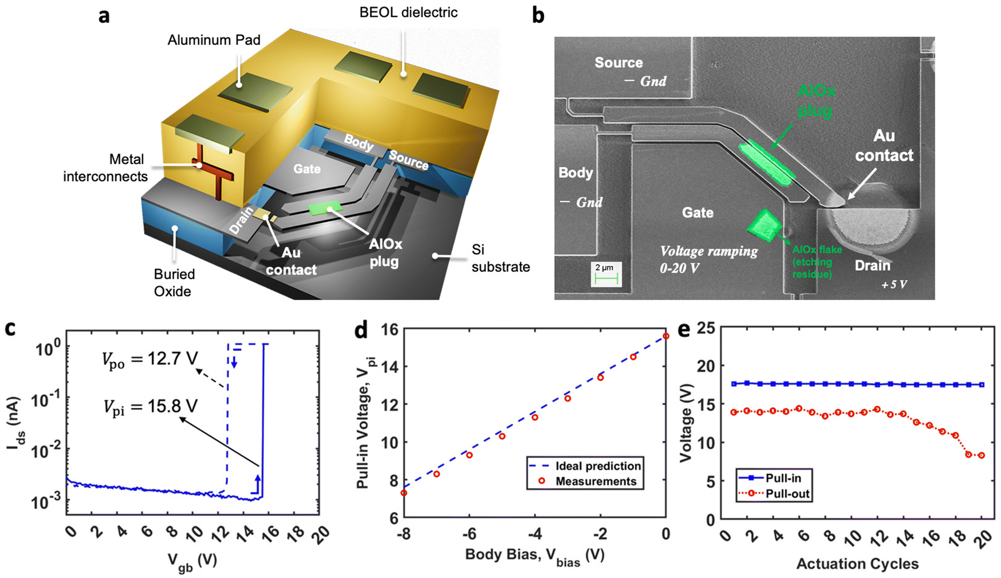 | ||
| Fig. 1 (a) 3-Dimensional (3D) schematic view of the 4-T NEM relay featuring four independent terminals, integrated with metal interconnect routings in the IMEC ISiPP50G foundry platform. (b) Top-view SEM micrograph of a partially released 4-T NEM relay with an Au coated contact tip featuring an 80 nm thick Au layer on the top surface and an estimated 30–35 nm thick Au layer on the sidewalls. (c) Measured actuation of an integrated 4-T NEM relay. The abrupt drain–source current increase and decrease indicate successful pull-in and pull-out. (d) Reduction of pull-in voltage with body-biasing. (e) Characterization of pull-in and pull-out voltages during 20 hot switching cycles; the unchanging pull-in voltage shows that monocrystalline Si exhibits stable mechanical cycling, while the changing pull-out voltage is indicative of the wear of the metallic contact. In the measurements shown in (c to e), the current limit was set to 1 nA to avoid undesired stiction failures due to the softness of the Au contact. | ||
Throughout the actuation process, the currents at the body terminal remained at the noise level (see Fig. S1e†), verifying that the two movable beams remained electrically isolated by the dielectric plug. We then cycled the NEM relay over 20 consecutive hot-switching cycles with a 1 nA current limit and a 5 V drain bias applied and monitored the evolution of Vpi and Vpo without body-biasing. As shown in Fig. 1e, Vpi has a variance of ∼3 mV during 20 cycles, which indicates stable pull-in behaviour of the Si NEM relay. Nonetheless, it is noteworthy that we observed a significant change of Vpo with cycling, which most likely is a result of the deterioration of the Au contact.20 After 20 cycles, the contact resistance of the 4-T relay increased significantly, resulting in a low drain current Ids. In the six devices we measured, Vpi was observed to fall within a range of 16 V ± 2 V (measurement data provided in Fig. S1a–d†), which most likely was due to contact variability, requiring a degree of gate overdrive to compensate. In four of the devices the contacts became stuck on the Drain after one cycle, most likely caused by the higher currents used in these measurements, which can cause micro-welding of the Au contact. Contact degradation, manifesting as increasing resistance with cycling, and micro-welding are expected from Au contacts,20 which was the simplest contact material available in our lab to prove the concept of our miniaturized, integrated 4-T NEM relay. For practical NEM relay utilization in low-power logic circuits, it is critical to achieve good relay contact reliability at the drain–source current of an order of 100 nA (see ESI section 1†). This cannot be easily accomplished with Au contacts,21 and therefore requires more durable relay contact materials, such as carbon-based coatings,22,23 hard metals such as Ti, TiN,24 W25 or Ru,26–28 or metal pairs such as Au–Ru.29 For example, it has been demonstrated that NEM relays with amorphous carbon coated contacts can switch over 100 million cycles at drain–source currents exceeding 1 μA.22
To enable the realization of VLSI NEM relay-based logic circuits, integrated 4-T NEM relays have to be manufacturable using high-yield, foundry-compatible processes. We structured our 4-T NEM relays and interconnects in the commercial SOI foundry process iSiPP50G offered by IMEC18 as depicted in Fig. 2a, with a subsequent post-foundry process as shown in Fig. 2b, to realize the dielectric plugs between the body and source beams, the contact tip metallization, and the suspension of the movable beams of the 4-T NEM relays. First, the 4-T relays were patterned in foundry FEOL processing using stepper lithography on top of an SOI wafer with a 220 nm thick Si device layer and a 2 μm thick layer of buried oxide (BOX) (Fig. 2a, steps i and ii). Then, a conventional 2-layer metal interconnect stack was deposited on top (Fig. 2a, step iii). In the next step, the BEOL oxide layers above the NEM relays were opened to create a cavity and expose the devices (Fig. 2a, step iv). At this stage, the wafers were shipped out from the IMEC foundry and the remaining process steps were carried out in university cleanrooms. One of the critical challenges in 4-T NEM relays is the realization of the dielectric plugs between the Body and Source beams, which we realized in post-processing steps. While the plug formation is more straightforward to establish for out-of-plane relays with layer-by-layer deposition,2 it has never been realized for in-plane 4-T relays at the nanoscale. Here, we developed a single-lithography process to create an in-plane dielectric plug while also protecting the BEOL stack from the vapor hydrofluoric acid (vHF) that was used for the sacrificial etching to suspend the relay beam. For the dielectric plug we chose AlOx due to its good mechanical performance and electrical isolation, compatibility with existing foundry processes, and excellent resistance to vHF etching. Thus, in the post-foundry process, we first deposited a thin layer (∼70 nm) of AlOx on top of the pre-fabricated foundry wafer using atomic layer deposition (ALD) (Fig. 2b, step I). Then, we patterned the AlOx layer with a standard buffered hydrofluoric acid (BHF) etching process using maskless laser lithography, to define the dielectric plug and selectively remove the AlOx in the region inside the cavities (Fig. 2b, step II). As the contact area is a critical parameter that affects surface adhesion forces, and thus Vpo, we developed a process that allows for full (see Fig. 3a and b) or partial Au metallization (see Fig. 3c and d) of the relay tip contacts. This process uses a single photolithography lift-off process to selectively expose the pre-defined relay contact regions for the subsequent Au deposition and lift-off (Fig. 2b, step III). Finally, the NEM relay beams were fully suspended by etching the BOX below the beams using vHF at a pressure of 14 Torr (Fig. 2b, step IV). Details of the dielectric AlOx plug formation and Au contact metallization processes are provided in ESI, section 2,† and information confirming the AlOx plug integrity is provided in ESI, section 1.†
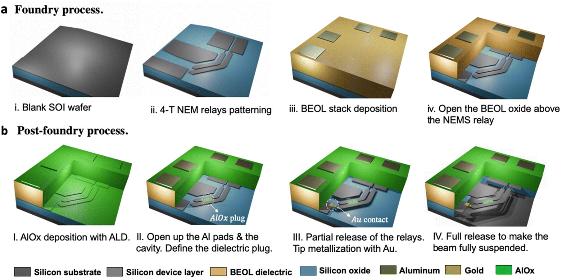 | ||
| Fig. 2 (a) 3D schematic of the manufacturing process flow for the integrated 4-T NEM relays. (a) Foundry process performed in the IMEC iSiPP50G platform. (i) Blank SOI wafer; (ii) patterning of 4-T NEM relay; (iii) BEOL stack deposition; (iv) opening the BEOL oxide above the relays to define the NEM cavities. (b) Post-foundry process. (I) AlOx passivation. (II) Opening up the Al pads and the NEM cavities, and definition of the dielectric (AlOx) plugs; (III) partial release etch of the NEM relay structures and subsequent relay contact tip metallization with Au; (IV) release etch to fully suspend the source and body terminals of the relays. | ||
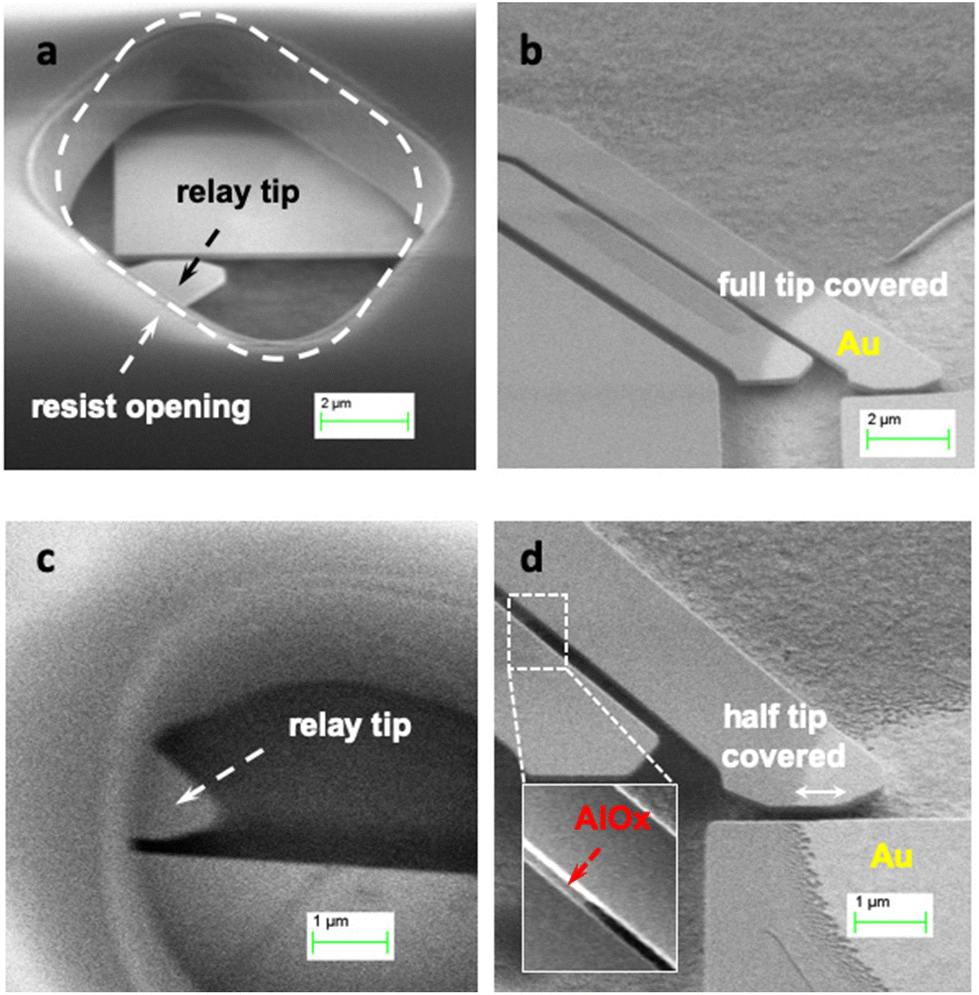 | ||
| Fig. 3 (a) SEM image of the tip window opening in a photoresist lift-off mask of a relay with full contact tip metallization, implemented using maskless laser lithography. (b) SEM image of the full contact tip Au metallization of a relay after the lift-off and before the full NEM relay release. (c) SEM image of the window opening in a photoresist lift-off mask of a relay with 50% (half) contact tip metallization, implemented using direct laser writing lithography. (d) SEM image of the 50% (half) contact tip metallization of a relay after the lift-off and before the full NEM relay release. The inset shows a close-up view of a part of the AlOx plug connecting the two beams of the relay. | ||
In designing NEM relay tip contacts, an essential parameter that affects the pull-out behaviour is the contact adhesion force (Fadh), which is proportional to the effective contact area30 (Aeff). If Fadh is larger than the spring restoring force (Fk), the contact will get stuck on the Drain after pull-in, which is a common relay failure mode. To prevent this failure, Fadh can be lowered by reducing the effective tip contact area Aeff. As a proof-of-concept for this solution, we analysed the pull-in and pull-out behaviour of one of our half-tip 4-T NEM relays, as shown in Fig. 3d. This particular half-tip relay exhibited repeatable pull-in and pull-out, at 17.5 V and 14 V, respectively, measured with a 1 nA current limit (see Fig. S1c, device sw4†). These results show that the adhesion force with half contact tip Au metallization is smaller than the restorative force of the relay hinge. To better understand the impact of the contact adhesion force on the pull-out behaviour, we developed a finite-element model (FEM) of our 4-T NEM relay in Ansys using a coupled field electrostatic simulation (see ESI, section 3† for design principles and relay design parameters). First, we confirmed that the pull-in voltage of the FEM (Vpi,sim = 17.8 V) strongly correlates with the measured actuation (Vpi = 17.5 V). Next, we simulated the contact adhesion force Fadh in the FEM model and extracted the pull-out voltage while varying Fadh from 0 to 140 nN, with which we generated a curve illustrating the relationship between Vpo and Fadh, shown in Fig. 4a. For low Fadh, the relay exhibits high Vpo and low hysteresis. However, as Fadh increases, Vpo drops rapidly which leads to high hysteresis. Once the adhesion force surpasses 96 nN, the pull-out voltage drops to zero, suggesting that the relay becomes stuck on the Drain. Thus, this curve provides design insight into how the adhesion force can be optimized to ensure reliable pull-out.
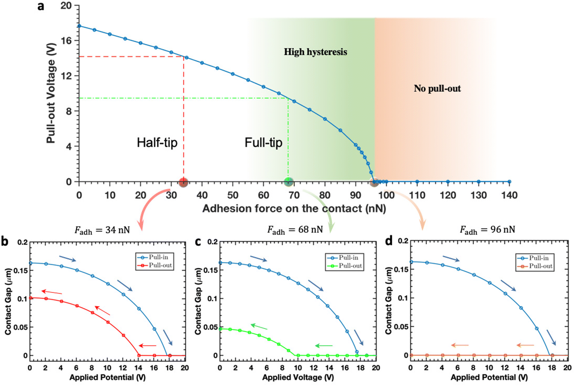 | ||
| Fig. 4 Finite-element model (FEM) simulations of 4-T NEM relay. (a) Simulation of the relationship between pull-out behaviour and adhesion force. (b) FEM actuation curve of the half-tip 4-T NEM relay, with Fadh = 34 nN. (c) FEM actuation curve of the full-tip 4-T NEM relay, with doubled Fadh = 68 nN. (d) FEM actuation curve of the 4-T NEM relays in the no pull-out regime. | ||
Given that the measured pull-out voltage of the half-tip 4-T NEM relay is 14 V, we infer from the simulated curve that the estimated Fadh of this relay is approximately 34 nN. The simulated pull-in and pull-out behaviour of the half-tip NEM relay is shown in Fig. 4b. Considering the linear relationship between Fadh and Aeff, we estimated that a full-tip 4-T NEM relay should have twice the adhesion force, resulting in 68 nN. Thus, our simulation suggests that the pull-out voltage of the full-tip relay should be around 9.1 V, as shown in Fig. 4c. Finally, this simulation also allows us to extract the point of no pull-out, which is at 96 nN. Above this point the restoring spring force of the relay hinge is insufficient to overcome Fadh and the switch gets stuck, which is confirmed in the simulated relay behaviour in Fig. 4d.
Thus, our simulations indicate that the 4-T NEM relays with half-tip Au metallization offers reliable pull-in and pull-out behaviour with low hysteresis, which is important for logic devices, as it reduces the noise margin between the discrete logic levels. These findings also suggest that decreasing the effective contact area Aeff serves as a viable strategy for reducing the hysteresis in NEM relays and enhancing their reliability. Further, the ability to carry out metallization with variable tip coverage provides an important tool to adjust the effective contact area after fabrication, based on application specific requirements. This is similar to mask-programmable circuits31 which are prefabricated in batches and customised for different specifications by a few process steps.
Conclusions
We demonstrated the first integrated Si 4-T NEM relays fabricated in a commercial SOI foundry platform, addressing the challenges of miniaturization and integration for practical 4-T NEM circuit applications. Our innovative process for creating an in-plane dielectric plug and partial contact metallization has enabled true 4-T functionality at the nanoscale. The realized 4-T NEM relays exhibited repeatable switching behaviour and functional body-biasing, which allowed for a linear reduction in pull-in voltage. Our NEM relay integration approach allows us to seamlessly incorporate the Si NEM relays into an existing SOI foundry platform, eliminating the need for the more complex wafer bonding and layer transfer processes required for existing heterogeneous 3D integration and stacking solutions. The potential also exists to integrate transistor-based functions in the same plane (i.e., in the Si device layer of the SOI substrate) as the Si NEM relays, which is not easily possible using alternative NEM relay integration approaches, and which could enable very high integration densities of transistor and NEM relay-based circuits. Although the contact reliability of the NEM relays have to be further optimized by investigating alternative contact materials, our results represent a significant milestone in the development of NEM-relay based logic circuits. By leveraging a commercial SOI foundry process and post-foundry steps compatible with wafer-level processing, we have lowered the threshold for commercialization and opened up new possibilities in the development of ultra-low power and highly integrated NEM relay-based logic circuits in the semiconductor industry.Author contributions
Y. L., S. J. B., and F. N. conceived this work. F. N. and K. B. G. supervised the project. W. B. coordinated the MORPHIC project, built the custom design environment, conceived and supervised the aggregation of the layouts. P. V. supervised and performed the device fabrication at IMEC. N.Q., F.N. and S. J. B. led, and A. Y. T., Y. L. and P. E. performed the development of the NEM post-processing, and characterization of the NEM devices. E. W. performed the theoretical modelling. S. J. B., E. W., M. K. K, Q. T., and D. P. designed and optimized the NEM structures, the contacts and the dielectric plug. All of the authors discussed and analysed the results. Y. L. and S. J. B. wrote the manuscript with input from all of the authors.Conflicts of interest
The authors declare no competing financial interest.Acknowledgements
Support from the European Union's Horizon 2020 research and innovation program under grant agreement No. 780283 (MORPHIC) and No. 871740 (ZeroAMP) is gratefully acknowledged. The authors acknowledge the support of the EPFL Center of MicroNanoTechnology (CMi) for process steps performed at EPFL.References
- M. Spencer, F. Chen, C. C. Wang, R. Nathanael and H. Fariborzi, et al., Demonstration of Integrated Micro-Electro-Mechanical Relay Circuits for VLSI Applications, IEEE J. Solid-State Circuits, 2011, 46(1), 308–320 Search PubMed.
- Y.-H. Song, D.-H. Choi, H.-H. Yang and J.-B. Yoon, An Extremely Low Contact Resistance MEMS Relay Using Meshed Drain Structure and Soft Insulating Layer, J. Microelectromech. Syst., 2011, 20(1), 204–212 Search PubMed.
- T. Qin, S. J. Bleiker, S. Rana, F. Niklaus and D. Pamunuwa, Performance Analysis of Nanoelectromechanical Relay-Based Field-Programmable Gate Arrays, IEEE Access, 2018, 6, 15997–16009 Search PubMed.
- S. Rana, J. Mouro, S. J. Bleiker, J. D. Reynolds, H. M. Chong, F. Niklaus and D. Pamunuwa, Nanoelectromechanical Relay without Pull-in Instability for High-Temperature Volatile Memory, Nat. Commun., 2020, 11, 1181 CrossRef CAS PubMed.
- T. Cao, T. Hu and Y. Zhao, Research Status and Development Trend of MEMS Switches: A Review, Micromachines, 2020, 11, 694 CrossRef PubMed.
- Y.-H. Yoon, Y. Jin, C.-K. Kim, S. Hong and J.-B. Yoon, A Low Contact Resistance 4-Terminal Mems Relay: Theoretical Analysis, Design and Demonstration, J. Microelectromech. Syst., 2018, 27, 497 CAS.
- R. Nathanael, V. Pott, H. Kam, J. Jeon and T. K. Liu, 4-Terminal Relay Technology for Complementary Logic, IEEE IEDM Tech. Dig., 2009, 223–226 Search PubMed.
- D. Lee, W. S. Lee, C. Chen, F. Fallah, J. Provine, S. Chong, J. Watkins, R. T. Howe, H.-S. P. Wong and S. Mitra, Combinational Logic Design Using Six-Terminal NEM Relays, IEEE Trans. Comput., 2013, 32, 653 Search PubMed.
- J. D. Reynolds, S. Rana, E. Worsey, Q. Tang, M. K. Kulsreshath, H. M. H. Chong and D. Pamunuwa, Single-Contact, Four-Terminal Microelectromechanical Relay for Efficient Digital Logic, Adv. Electron. Mater., 2022, 2200584 Search PubMed.
- J.-O. Lee, M.-W. Kim, S.-D. Ko, H.-O. Kang, W.-H. Bae, M.-H. Kang, K.-N. Kim, D.-E. Yoo and J.-B. Yoon, 3-Terminal Nanoelectromechanical Switching Device in Insulating Liquid Media for Low Voltage Operation and Reliability Improvement, IEDM Tech. Dig., 2009, 227–230 Search PubMed.
- R. Nathanael, V. Pott, H. Kam, J. Jeon and T.-J. K. Liu, 4-terminal Relay Technology for Complementary Logic, IEDM Tech. Dig., 2009, 204–207 Search PubMed.
- H. Kam, V. Pott, R. Nathanael, J. Jeon, E. Alon and T.-J. K. Liu, Design and Reliability of a Micro-relay Technology for Zero-standby Power Digital Logic Applications, IEDM Tech. Dig., 2009, 757–760 Search PubMed.
- R. Gaddi, R. V. Kampen, A. Unamuno, V. Joshi, D. Lacey, M. Renault, C. Smith, R. Knipe and D. Yost, MEMS Technology Integrated in The CMOS Back-end, Microelectron. Reliab., 2010, 1593–1598 CrossRef CAS.
- J. Jeon, V. Pott, H. Kam, R. Nathanael, E. Alon and T.-J. K. Liu, Perfectly Complimentary Relay Design for Digital Logic Applications, IEEE Electron Device Lett., 2010, 31(4), 371–373 CAS.
- Y. Li, S. J. Bleiker and P. Edinger, et al., Design and fabrication of a 4-terminal in-plane nanoelectromechanical relay, Transducers, 2023, Kyoto, Japan.
- P. P. Absil, P. D. Heyn, H. Chen, P. Verheyen, G. Lepage, M. Pantouvaki, J. D. Coster, A. Khanna, Y. Drissi; D. V. Thourhout and J. V. Campenhout, Imec iSiPP50G silicon photonics: a robust CMOS-based photonics technology platform, SPIE OPTO, 2015, San Francisco, California, United States.
- M. Pantovaki, S. A. Srinivasan, Y. Ban, P. D. Heyn, P. Verheyen, G. Lepage, H. Chen, J. D. Coster, N. Golshani, S. Balakrishnan, P. Absil and J. V. Campenhout, Active Components for 50 Gb/s NRZ-OOK Optical Interconnects in A Silicon Photonics Platform, J. Lightwave. Technol., 2017, 35, 631–638 Search PubMed.
- N. Quack, A. Y. Takabayashi and H. Sattari, et al., Integrated silicon photonic MEMS, Microsyst. Nanoeng., 2023, 9, 27 CrossRef CAS PubMed.
- G. Jo, P. Edinger, S. J. Bleiker, X. Wang, A. Y. Takabayashi, H. Sattari, N. Quack, M. Jezzini, J. S. Lee, P. Verheyen, I. Zand, U. Khan, W. Bogaerts, G. Stemme, K. B. Gylfason and F. Niklaus, Wafer-level Hermetically Sealed Silicon Photonic MEMS, Photonics Res., 2022, 10(2), A14–A21 CrossRef.
- S. T. Patton and J. S. Zabinski, Fundamental studies of Au contacts in MEMS RF switches, Tribol. Lett., 2005, 18(2), 215–230 CrossRef CAS.
- A. Peschot, C. Qian and T. J. K. Liu, Nanoelectromechanical Switches for Low-Power Digital Computing, Micromachines, 2015, 6, 1046–1065 CrossRef.
- D. Grogg, C. Ayala, U. Drechsler, A. Sebastian, W. Koelmans, S. J. Bleiker, et al., Amorphous carbon active contact layer for reliable nanoelectromechanical switches, IEEE MEMS, 2014, San Francisco, CA, USA, pp. 143–146.
- S. Rana, J. D. Reynolds, T. Y. Ling, M. S. Shamsudin, S. H. Pu, H. M. Chong and D. Pamunuwa, Nano-crystalline graphite for reliability improvement in MEM relay contacts, Carbon, 2018, 133, 193–199 CrossRef CAS.
- C. Oh and M. P. De Boer, Optimization and contact reliability of TiN-coated microswitches in various gas environments, J. Microelectromech. Syst., 2019, 28(1), 95–106 CAS.
- E. Falicov, Breakdown and healing if Tungsten-Oxide films on microelectromechanical relay contacts, J. Microelectromech. Syst., 2022, 31(2), 265–274 Search PubMed.
- L. Chen, H. Lee, Z. J. Guo, N. E. McGruer, K. W. Gilbert, S. Mall, K. D. Leedy and G. G. Adams, Contact resistance study of noble metals and alloy films using a scanning probe microscopy test station, J. Appl. Phys., 2007, 102, 074910 CrossRef.
- M. Walker, C. Nordquist, D. Czaplewski, G. Patrizi, N. McGruer and J. Krim, Impact of in situ oxygen plasma cleaning on the resistance of Ru and Au–Ru based RF microelectromechanical system contacts in vacuum, J. Appl. Phys., 2010, 107, 084509 CrossRef.
- S. M. Karabanov, D. V. Suvorov, G. P. Gololobov, V. S. Gurov, D. Y. Tarabrin and E. V. Slivkin, Long-time stability of electrical contact base on ruthenium nanoscale films at various coating roughness, IEEE RTSI, 2015, pp. 39–43.
- T. Laurvick, C. Stilson and R. Coutu, Experimental investigation of thin film spreading resistance in microcontacts, IEEE Holm., 2014, New Orleans, LA, 1–6.
- J. N. Israelachvili, Intermolecular and Surface Forces, Academic, San Francisco, CA, USA, 3rd edn, 2011 Search PubMed.
- J. M. Rabaey, A. P. Chandrakasan and B. Nikolic, Digital integrated circuits, Englewood Cliffs, Prentice hall, 2002, vol. 2 Search PubMed.
Footnotes |
| † Electronic supplementary information (ESI) available. See DOI: https://doi.org/10.1039/d3nr03429a |
| ‡ Present address: University of Sydney, 2006, NSW, Australia. |
| This journal is © The Royal Society of Chemistry 2023 |