
Unravelling the room temperature growth of two-dimensional h-BN nanosheets for multifunctional applications†
Abhijit
Biswas‡
 *a,
Rishi
Maiti‡
b,
Frank
Lee‡
c,
Cecilia Y.
Chen
d,
Tao
Li
e,
Anand B.
Puthirath
a,
Sathvik Ajay
Iyengar
a,
Chenxi
Li
a,
Xiang
Zhang
a,
Harikishan
Kannan
a,
Tia
Gray
a,
Md Abid Shahriar Rahman
Saadi
a,
Jacob
Elkins
a,
A. Glen
Birdwell
f,
Mahesh R.
Neupane
f,
Pankaj B.
Shah
f,
Dmitry A.
Ruzmetov
f,
Tony G.
Ivanov
f,
Robert
Vajtai
a,
Yuji
Zhao
e,
Alexander L.
Gaeta
*bd,
Manoj
Tripathi
*c,
Alan
Dalton
c and
Pulickel M.
Ajayan
*a
*a,
Rishi
Maiti‡
b,
Frank
Lee‡
c,
Cecilia Y.
Chen
d,
Tao
Li
e,
Anand B.
Puthirath
a,
Sathvik Ajay
Iyengar
a,
Chenxi
Li
a,
Xiang
Zhang
a,
Harikishan
Kannan
a,
Tia
Gray
a,
Md Abid Shahriar Rahman
Saadi
a,
Jacob
Elkins
a,
A. Glen
Birdwell
f,
Mahesh R.
Neupane
f,
Pankaj B.
Shah
f,
Dmitry A.
Ruzmetov
f,
Tony G.
Ivanov
f,
Robert
Vajtai
a,
Yuji
Zhao
e,
Alexander L.
Gaeta
*bd,
Manoj
Tripathi
*c,
Alan
Dalton
c and
Pulickel M.
Ajayan
*a
aDepartment of Materials Science and Nanoengineering, Rice University, Houston, Texas 77005, USA. E-mail: abhijit.biswas@rice.edu; ajayan@rice.edu
bDepartment of Applied Physics and Applied Mathematics, Columbia University, New York, 10027, USA. E-mail: a.gaeta@columbia.edu
cDepartment of Physics and Astronomy, University of Sussex, Brighton BN1 9RH, UK. E-mail: m.tripathi@sussex.ac.uk
dDepartment of Electrical Engineering, Columbia University, New York, 10027, USA
eDepartment of Electrical and Computer Engineering, Rice University, Houston, TX 77005, USA
fDEVCOM Army Research Laboratory, RF Devices and Circuits, Adelphi, Maryland 20783, USA
First published on 21st February 2023
Abstract
The room temperature growth of two-dimensional van der Waals (2D-vdW) materials is indispensable for state-of-the-art nanotechnology. Low temperature growth supersedes the requirement of elevated growth temperatures accompanied with high thermal budgets. Moreover, for electronic applications, low or room temperature growth reduces the possibility of intrinsic film-substrate interfacial thermal diffusion related deterioration of the functional properties and the consequent deterioration of the device performance. Here, we demonstrated the growth of ultrawide-bandgap boron nitride (BN) at room temperature by using the pulsed laser deposition (PLD) process, which exhibited various functional properties for potential applications. Comprehensive chemical, spectroscopic and microscopic characterizations confirmed the growth of ordered nanosheet-like hexagonal BN (h-BN). Functionally, the nanosheets show hydrophobicity, high lubricity (low coefficient of friction), and a low refractive index within the visible to near-infrared wavelength range, and room temperature single-photon quantum emission. Our work unveils an important step that brings a plethora of potential applications for these room temperature grown h-BN nanosheets as the synthesis can be feasible on any given substrate, thus creating a scenario for “h-BN on demand” under a frugal thermal budget.
New conceptsThe growth of two-dimensional van der Waals materials at low/room temperature is indispensable for state-of-the-art nanotechnology as it supersedes the requirement of an elevated growth temperature that comes with additional high thermal budgets (and with the possibility of an increase of interfacial thermal diffusion). Here, two-dimensional hexagonal boron nitride (h-BN) nanosheets are grown at room temperature by a highly energetic pulsed laser deposition (PLD) growth technique, exhibiting remarkable functional properties and suitability for a number of applications (e.g. hydrophobicity, a low refractive index in the visible wavelength range, low frictional force, and remarkable room temperature single-photon emission), thus creating a potential scenario for “h-BN on demand” under a frugal thermal budget, which is indispensable for nanotechnology. |
Introduction
Two-dimensional van der Waals (2D-vdW) materials are astonishing in the nano-era, showing tremendous potential and technological relevance due to their unique atomic-scale growth, emergent functional properties, and application potential.1–4 In general, several top-down (chemical, and mechanical exfoliations) and bottom-up approaches (thin films growth by various physical/chemical vapor phase deposition techniques) have been employed to synthesize these 2D-vdW materials with atomic layer control.5–7 Among these, the liquid exfoliation methods produce large-area 2D-vdW materials; however, the film quality is found to be very low (due to the presence of adsorbates and surfactants on the surface). Whereas vapor-phase thin film growth processes lead to smaller sized crystals, but with high crystalline quality.8 Due to this process-dependent variable quality, the growth of 2D-vdW materials thus remains an exceedingly intriguing research topic among the materials growth community. The formation, crystallinity, morphology, and consequent functional properties of 2D-vdW materials are highly sensitive to the thermodynamic and/or growth kinetics, the adsorption of the reactive species on the substrate surface, nucleation, and thus the resultant film growth and its consequent properties.9,10Among various procedures, for large-scale growth, intrinsic property evaluation, and nano-device fabrication, chemical vapor deposition (CVD) has widely been adopted to grow 2D-vdW materials.5,6 However, synthesizing 2D-vdW materials by CVD requires a very high-temperature of ∼1000–1500 °C (for a sufficient supply of activation energy to the adatoms so that they can migrate to the energetically preferred locations on the substrates during growth); a rigorous synthesizing condition that limits device capabilities as elevated temperatures result in possible defect segregation and annihilation at the interfaces.11–14 Therefore, researchers are trying to synthesize 2D-vdW materials at relatively low-temperatures, with a trade-off between crystalline domain size/quality and generating novel application possibilities.15–18 Theoretically, 2D materials show anisotropy in growth and kinetics that can be controlled by adjusting the balance between elements.19 However, fundamentally, both thermodynamics (temperature) and kinetics play important roles, therefore the temperature during the vapor-phase deposition has always been critical, which also affects the nucleation density and grain size.10,15 Therefore, the growth of 2D-vdW materials at lower temperatures or even at room temperature with a high-enough supply of kinetic energy directed towards the reaction species might be sufficient to overcome the nucleation barrier, and if successful, it would be very useful for several room-temperature applications. This would significantly enable the growth of 2D-vdW materials on any given substrate (with varying degrees of crystallinity, thickness, and uniformity and their consequent emergent phenomena), creating a scenario for “thin films growth of 2D-vdW materials on demand”, thereby leading to ample investigations of their properties and their consequent applications.
To investigate this possibility of thin film room-temperature growth, we use hexagonal boron nitride (h-BN) as our model material. Among numerous 2D-vdW materials, ultra-wide bandgap h-BN (with a bandgap of ∼5.9 eV) gets special attention for its excellent chemical inertness, high-thermal stability, and electronic, optical, and mechanical properties.20,21 Electronically, h-BN is suitable as a gate-dielectric layer for 2D-based field effect transistor (FET) devices.22 The high bandgap of h-BN makes it suitable for the fabrication of high-performance deep-ultraviolet photodetectors.23 Moreover, the weak inter-layer bonding in h-BN makes it a soft lubricant material and thus useful as high-temperature corrosion resistant and antioxidation protective coatings for various industrial applications.21 Given these advantages, we attempt to grow h-BN thin films at room temperature by using a highly energetic and thermally non-equilibrium thin film growth process, pulsed laser deposition (PLD). PLD possesses several advantages over other growth methods as it is not in thermal equilibrium, directed onto the substrate, and the stoichiometry is preserved throughout the thin film deposition process, starting from a dense crystalline target of the desired material.24 Several attempts have been implemented to grow h-BN films by PLD; however, at elevated temperatures, they show mostly island-like growth.25–30 The plasma formation during the ablation process of the target by pulsed UV-laser (photon energy of ∼5 eV) contains radicals and ions (e.g. B+, N+, N*, N2, N2+, N2* and B*N+) of the ablated species with kinetic energy ∼10–100 eV (Fig. 1a and b).31
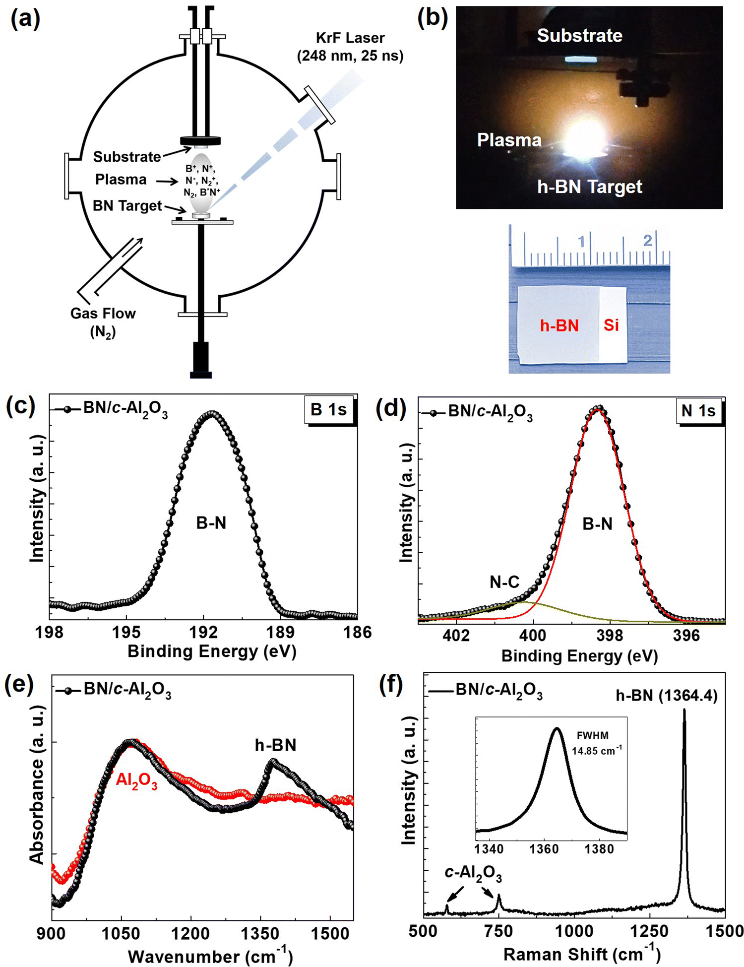 | ||
| Fig. 1 Pulsed laser deposition of h-BN and its spectroscopic characterizations. (a) Schematic showing the thin film growth process by pulsed laser deposition. (b) Real-time plume generation (highly energetic) during the ablation of h-BN with ablated species deposited on a substrate kept at room temperature. An optical image of a uniform (∼1 × 1 cm2) thick h-BN film (bottom). (c) and (d) XPS elemental B 1s and N 1s core scans on c-Al2O3 confirm the presence of characteristics B–N bonds. (e), (f) FTIR and Raman spectra shows the peak at ∼1364 cm−1, further confirming the growth of h-BN at room temperature. | ||
We have grown h-BN at room temperature on various substrates: c-Al2O3 (0001), a holey Cu-grid, and Si (100), and investigated their growth characteristics and several functional properties. Chemical, morphological, spectroscopic, and electron microscopy characterizations confirm the growth of ordered h-BN nano-sheets. We observed that the films are hydrophobic, and exhibit a low-refractive index, and room temperature single-photon quantum emission. Moreover, the frictional characteristics reveal excellent lubrication properties with a low coefficient of friction. Thus, successful growth of ordered h-BN nano-sheets by PLD at room temperature might lead to the growth of h-BN on a variety of substrates, generating ample potential applications under reduced thermal budgets, e.g. for flexible 2D-electronics,32 coating layers for highly-corrosive materials, protecting layers for open-air degradable materials, precise photonic devices and for quantum information technology.
Results and discussion
Structurally, to characterize the grown h-BN films we first performed conventional B 1s and N 1s core-level X-ray photoelectron spectroscopy (XPS) elemental scans. Characteristically, we observed the B–N bonding-related peaks in both the elemental B 1s (at ∼190.6 eV) and N 1s (at ∼398.5 eV) core level scans with π-plasmon peaks (∼9 eV apart from the main B–N peak), which are characteristic of h-BN (Fig. 1c, d and Fig. S1a, S1b, ESI†).33 In the N 1s scans, in addition to the B–N bonding peak, we observed a small shoulder of the N–C peak at ∼400.5 eV (Fig. 1d), due to the ambient air exposure effect, related to adventitious carbon.34 Through the valence band spectra (VBS), we observed the characteristic band structure of the h-BN film (two distinct features with maxima at ∼12 and ∼20 eV, corresponding to the overlapping of the σ and π-bands as well as the s-band, respectively) with a valence band maxima (VBM) position at ∼1.7 eV (Fig. S1c, ESI†).35,36 In order to confirm the phase, we then performed Fourier transform infrared (FTIR) spectroscopy and Raman spectroscopy. FTIR shows a peak within the range 1350–1500 cm−1, attributed to the in-plane B–N stretching vibrations (transverse optical mode) of the sp2-bonded h-BN (Fig. 1e).37 Moreover, in the Raman spectra we observed a Raman-active in-plane E2g phonon mode at ∼1364 cm−1 (Fig. 1f),33 with a narrow full-width at half maximum (FWHM) of ∼14.85 cm−1, along with peaks at ∼577.4 and ∼749.2 cm−1, originating from the sapphire substrate. The Raman peak is slightly red shifted (∼2 eV) to lower phonon frequencies compared to the bulk h-BN (∼1366 eV), suggesting that the nanosheets are showing slight tensile strain.33 All these spectroscopic characterizations indicate the room-temperature growth of h-BN films.Hereafter, we investigated the surface morphology of the films by using atomic force microscopy (AFM). Interestingly, they show 2D nanosheet-like morphology (on c-Al2O3) (Fig. 2a). The lateral sizes of these h-BN sheets are ∼200–300 nm and the area coverage per 3 × 3 μm2 is nearly ∼70![[thin space (1/6-em)]](https://www.rsc.org/images/entities/char_2009.gif) 441.75 nm2 (Fig. S2, ESI†). Furthermore, to confirm the crystalline nature, we performed top-view high-resolution transmission electron microscopy (HRTEM) by growing h-BN films directly on a holey Cu grid. For HRTEM, we have grown ultra-thin h-BN by providing only a small number of laser shots (100 laser shots to be precise). As seen from the HRTEM images (Fig. 2b), we also observed nano-crystal-like features. We captured several images at different magnification levels and obtained the diffraction patterns and d spacing. Remarkably, a closer inspection shows the appearance of clear ordered lattice fringes (Fig. 2c). We obtained the d spacing which corresponds to the vdW gap between individual h-BN sheets (d0002 = 0.33 nm) with a hexagonal diffraction pattern, although the signals are very weak in intensity (Fig. 2d and Fig. S3, ESI†).20,21 The TEM images, corresponding diffraction patterns and d-spacing also show that along with the ordered hexagonal structure, a degree of amorphization (evident from the amorphous disk in the diffraction pattern) also exists in the nanosheets, at least for the ultrathin h-BN grown on the holey Cu-grid at room temperature.
441.75 nm2 (Fig. S2, ESI†). Furthermore, to confirm the crystalline nature, we performed top-view high-resolution transmission electron microscopy (HRTEM) by growing h-BN films directly on a holey Cu grid. For HRTEM, we have grown ultra-thin h-BN by providing only a small number of laser shots (100 laser shots to be precise). As seen from the HRTEM images (Fig. 2b), we also observed nano-crystal-like features. We captured several images at different magnification levels and obtained the diffraction patterns and d spacing. Remarkably, a closer inspection shows the appearance of clear ordered lattice fringes (Fig. 2c). We obtained the d spacing which corresponds to the vdW gap between individual h-BN sheets (d0002 = 0.33 nm) with a hexagonal diffraction pattern, although the signals are very weak in intensity (Fig. 2d and Fig. S3, ESI†).20,21 The TEM images, corresponding diffraction patterns and d-spacing also show that along with the ordered hexagonal structure, a degree of amorphization (evident from the amorphous disk in the diffraction pattern) also exists in the nanosheets, at least for the ultrathin h-BN grown on the holey Cu-grid at room temperature.
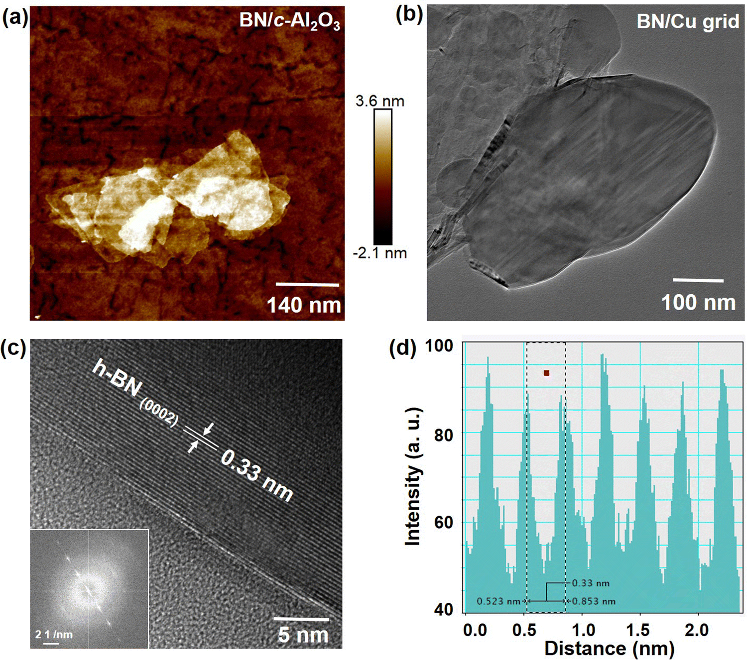 | ||
| Fig. 2 Microscopic characterizations of h-BN. (a) AFM topography shows the nanosheet-like growth. (b) and (c) High-resolution transmission electron microscopy (HRTEM) also shows the sheet-like structure with the corresponding diffraction pattern (inset). (d) Inter-planar d spacing of ∼0.33 nm, corresponding to the (0002) lattice plane of h-BN. For HRTEM, a few shots of BN were supplied directly on the holey Cu grid. | ||
As mentioned earlier, the room temperature growth of highly ordered nanosheets is extremely interesting and cost-effective for scale-up, as they can be grown on potentially any given substrate (e.g. foils, flexible polymer surfaces), widening the horizon of h-BN growth for applications.20 There have been attempts to grow h-BN at room temperature by RF sputtering and atomic layer deposition (ALD), but these attempts have formed an amorphous/turbostratic phase.38,39 In the case of PLD, which is most often used for metal-oxide thin film depositions, it is well known that a high-temperature (≥700 °C) is needed for epitaxial growth (depending on the thermodynamics).24 However, as reported by Elhamid et al., well-defined graphene can be grown at room temperature by PLD on a bi-metallic Ni–Cu substrate, where the laser power played a crucial role, favoring a nucleation activation energy which promotes graphene formation.40 Rasic et al. grew metallic TiN thin films on sapphire at room-temperature.41 Kakehi et al. reported the epitaxial growth of NiO (111) thin films by PLD at room-temperature.42 Ma et al. grew ZnO films on glass at room temperature by PLD.43 Fundamentally, the adsorption energy is one order higher than the diffusion energy barrier and at lower temperature, the adsorption rate exceeds the desorption rate.15 Therefore, small-fractal shaped domain growth has been observed for the vapor-phase synthesis of 2D materials at high flux and reduced temperature.15 Very recently, people have also started putting in effort to grow h-BN at various temperatures by PLD.44 Hence, from a growth perspective, an energetic bombardment of particles during the growth process is necessary to synthesize h-BN films at lower/room temperature, with the ability for the adatoms to overcome the substrate diffusion energy barrier. Ideally, the thin film synthesis process involves: (1) evaporation and transport of the ablated species to the substrate, (2) migration of the ablated species onto the substrate, and (3) nucleation and crystal growth.24 For h-BN growth, the laser ablated species are atomic neutral and ionized species including B+, B*, N+, and N*, and molecular species including N2*, N2+, and B*N+.31 These species arrive concurrently on the substrate with a high kinetic energy of ∼10–100 eV, and thereby form h-BN layers (nanosheets in our case) within microseconds (∼2 μS) onto the substrate, even at room temperature. The importance of the substrate temperature is to supply additional energy for these species to mobilize onto the surface, coalesce, form bonds with the substrates, thus promoting better nucleation, and consequent crystallinity. We have also performed FESEM and grazing incident angle X-ray diffraction (GIXRD) of the h-BN target, before and after the laser ablation (Fig. S4, ESI†). In both cases, the FESEM images show similar morphology with a typical sheet size of several μm, which is much larger than the lateral sizes for the room temperature grown h-BN nanosheets, as shown in the AFM images (Fig. 3b). The GIXRD results show only the reduction in the (0002) h-BN peak intensity after laser ablation, which is apparent as the target surface becomes rougher after the ablation. Considering PLD is a highly energetic deposition process and in addition BN contains light elements, thus synergistically, created vapor pressure and kinetic energy of the laser-ablated species in the plasma form possibly sufficient to migrate to the substrate and nucleate onto it (within a few μS) and forms the films even at room temperature, affecting the nucleation density and grain size.15,24 All these observations reduce the possibility that growth happens due to the sputtering of nano-BN particles from the target, but rather it follows the typical thin film growth process, at least for the present employed growth protocols.
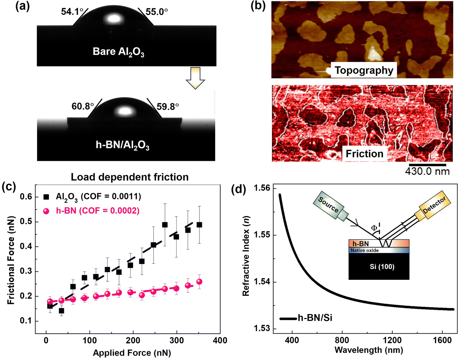 | ||
| Fig. 3 Functional properties of h-BN. (a) Contact angle measurements on the h-BN surface, showing the water repelling nature. (b) Topography (upper panel) and the corresponding frictional force (lower panel) map of h-BN/c-Al2O3. The darker colors in the frictional force map of the h-BN suggest lower friction. (c) The measured frictional force with different loading. The slope of the fitted line represents the coefficient of friction (COF) of the material. (d) The refractive index (n) of the h-BN film (grown on Si substrate). The inset shows the schematic of the measurement. | ||
To realize the intrinsic functional properties of the h-BN nanosheets, first, we investigate the wetting characteristics by contact angle (CA) measurements, as hydrophobic surfaces are known as effective protective layers in harsh environments with extreme temperatures, and h-BN provides strong resistance to chemical attack and high-temperature stability.20 As observed, h-BN tends toward minimizing the contact surface with water. The nanosheets exhibit hydrophobic behavior which is fairly increased by ∼5%, (CA: 55° ± 1 to 60° ± 1) (Fig. 3a), consistent with the polar character of the boron-nitrogen bond (–N−B+–), as the wettability is strongly influenced by the vdW interactions.45 The measured CA is also in agreement with the reported values ranging between ∼50–67°.45 Fundamentally, the wetting characteristics of a particular material also depend on the surface roughness and are inherent to the wetting phenomena.46,47 However, considering that the surface roughness of the grown h-BN nanosheets is of a few nm (∼2–3 nm), the effect of roughness on the CA may be insignificant here.
The effects of the hydrophobicity and inertness of the h-BN nanosheets are further investigated through force-distance (F-D) spectroscopy measurements and the associated line profile using an AFM probe covered with diamond-like carbon (DLC) (Fig. S5 and S6, ESI†). In the F-D measurements, the AFM probe temporarily brings a closer “repulsive regime” to the h-BN nanosheets for short durations (sub-seconds) and then moves away vertically from the surface. It requires work against the adhesion force that brings the cantilever away from the surface (i.e. h-BN nanosheet and c-Al2O3), referred to as a “pull-out” force. A higher value of the pull-out force indicates a vital interaction with the substrate towards the tip apex and vice versa. The h-BN nanosheets show smaller pull-out force values towards the DLC tip as compared to the host substrate corroborating the CA measurements.
At the submicron scale, the intrinsic roughness and moderately hydrophobic surface influence the tribological response. Thus, the frictional characteristics of h-BN (on c-Al2O3) are examined by lateral force microscopy where the topography and the corresponding frictional force map are measured at the same acquisition (Fig. 3b). The presence of h-BN layers may lead to the prediction of lower friction force values than the surrounded c-Al2O3 substrate. However, the edges and step-edges lead to the highest friction values due to the higher susceptibility of edge atoms towards the slider (tip apex) which is peculiar to the family of 2D-vdW materials.48,49 The tendency of the lubrication is further monitored where the probe sweeps the same region of h-BN and c-Al2O3 with an increasing applied normal force ranging from 10 nN to 350 nN (Fig. 3c). We observed a linear response of the increase in the friction force as a function of the normal forces, where the trend of load-dependent friction is higher for the alumina substrate as compared to h-BN, which is quantified through a linear fit resulting in the coefficient of friction (COF). The COF values of h-BN and c-Al2O3 are obtained as ∼0.0002 and ∼0.0011, respectively. The COF value depends on the nature of the material used and the local contact area between the tip apex and the substrate. Considering that the local contact area of the tip apex is similar while rubbing between h-BN and alumina surface in a single scan at fixed load conditions, it is the nature of the material dominating the higher COF values for alumina. The additional factor influencing the frictional behavior in 2D materials is the interfacial interaction with the host surface. It is observed that the c-Al2O3 plane is relatively reactive w.r.t. the other planes (e.g. a-Al2O3), to establish a stronger interfacial bond with h-BN.50 Weak vdW interactions (e.g. h-BN-silica, graphene-silica) lead to higher friction forces of the atomically thin sheets owing to the puckering effect “i.e. out-off plane deformation that resists sliding” compared to the thick layers.49 Whereas, a stronger interfacial interaction (i.e. graphene-mica, and graphene-Ni(111)) does not show the puckering effect, revealing that the frictional force response is independent of the thickness.51,52 We did not observe a thickness dependent frictional contrast in our friction map, indicating a stronger interaction between h-BN and c-Al2O3 (Fig. S2, ESI†). These results are in good agreement with conventionally fabricated h-BN nanosheets and other 2D materials.52–54 Overall, the observed hydrophobic nature and lubricity of the h-BN nanosheets would be useful for the coating industry.
Furthermore, we measured the refractive index (n) of a h-BN nanosheets grown on a Si substrate (see ESI† Fig. S7 for the detailed characterizations of the film), which was found to be ∼1.53–1.55 (Fig. 3d) within the visible and near-infrared spectral range. We used variable angle spectroscopic ellipsometry (VASE) to measure the refractive index (n). The schematic of the measurement is depicted in the inset of Fig. 3d. Considering the nanosheet-like morphology of h-BN, we fitted the ellipsometry data by applying the Bruggeman effective-media approximation (EMA) method that considers the film to be h-BN with defects (see the methods section and Fig. S8, ESI†). Interestingly, the h-BN with added voids into the fitting model provides a lower n than the perfect single crystalline layer h-BN fitting (n ∼ 1.8). The lower n is adequate as stoichiometry, porosity, and roughness affect the value of n.55,56 Interestingly, the lower n is helpful for the precise designing of photonic devices operating in the visible and near-infra-red wavelength range.55
Since h-BN nanosheets can host defects such as point defects (including boron-vacancies (VB) and/or nitrogen-vacancies (VN)), nitrogen-vacancies and boron replacing nitrogen (VNNB), and also carbon impurities, they may show single photon emission (SPE) at room temperature, attributed to these localized defect states inside the bandgap.57–61 SPE in h-BN is extremely important for next-generation quantum computing and information-processing technologies, considering its excellent chemical and thermal robustness.62,63Fig. 4a shows a confocal photoluminescence (PL) map (∼50 × 50 μm2) of h-BN nanosheets showing much brighter emission spots (yellow) above the background.
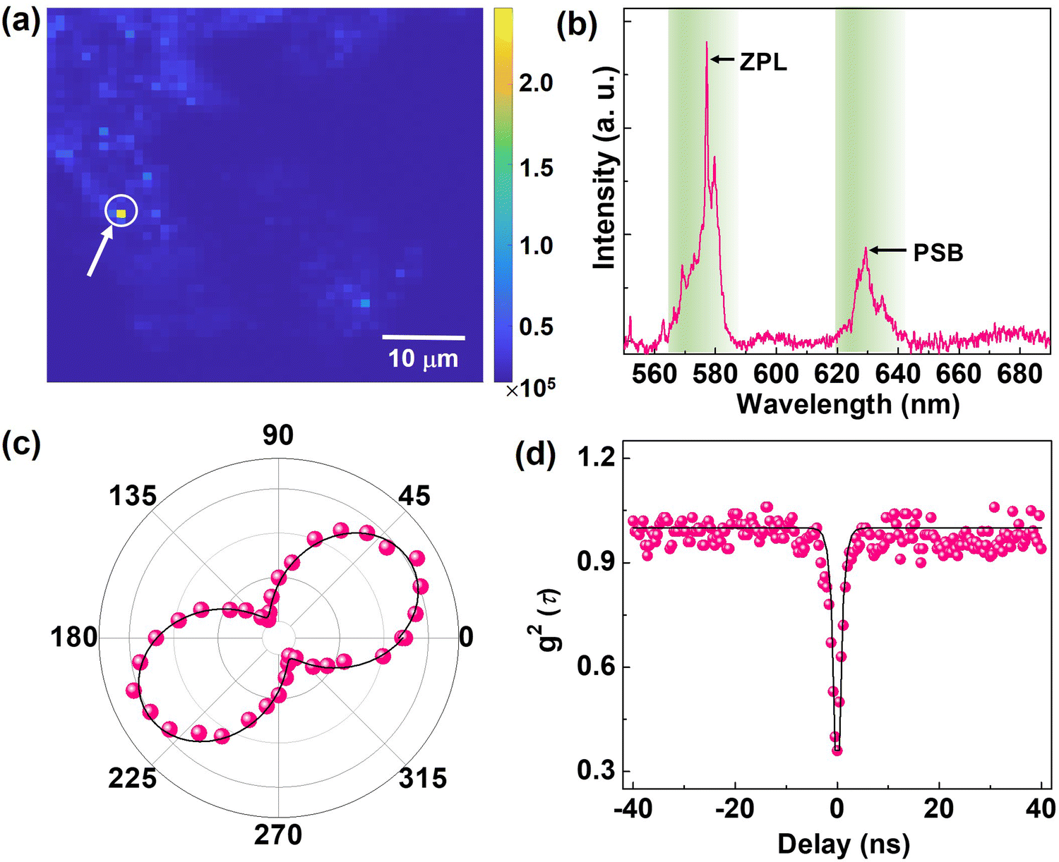 | ||
| Fig. 4 Room-temperature photo-physical properties of h-BN nanosheets. (a) Confocal photoluminescence map (∼50 × 50 μm2) corresponds to the ultra-bright (yellow spots) defect-assisted emission from the h-BN nano-sheets grown on sapphire. (b) Photoluminescence spectrum under 532 nm laser excitation and a 550 nm long-pass filter at room temperature. (c) The emission (red spheres) polarization curve. The red curve is fitted using a cos2θ function indicating an atomic defect with the in-plane dipole moment. (d) Second-order autocorrelation measurement g(2)(τ) of the defect with a dip at g(2)(0) ≈ 0.36, suggesting the antibunching nature of light. | ||
Fig. 4b shows the corresponding PL emission spectrum under continuous wave non-resonant excitation (λ = 532 nm). The emitter has a sharp zero-phonon line (ZPL) at ∼577 nm with an asymmetric shape (FWHM ∼2 nm), extracted from a single Lorentzian fit. A weak optical phonon replica is visible around ∼630 nm, and is red-shifted by ≥165 nm from the ZPL peak, which is related to the phonon sidebands (PSB).64 It should be noted that the small peak at ∼580 nm is most likely a ZPL of another weak emitter within the excitation spot. In order to understand the extent of the electron–phonon coupling we calculate the Debye–Waller factor (the ratio between ZPL intensity to the total emission) which is found to be ∼0.70.
In order to understand the polarization behavior of the localized emission, we performed emission polarization measurements. Fig. 4c corresponds to the angular diagram of emission, which reflects a well-defined dipole-like character for the single isolated defect. The corresponding fits are obtained using a cos2(θ) fitting function, which yields an emission polarization visibility of ∼75%, suggesting a single dipole transition linearly oriented along the basal plane of the h-BN nanocrystals. Fig. 4d displays the second-order correlation function g2(τ) using two Si APDs, mounted in a Hanbury–Brown and Twiss (HBT) configuration to establish the quantum nature of the emitted light from the defects of the h-BN nanocrystals. The g2(0) is found to be ∼0.36, well below 0.5 (without background correction) at zero delay time (Fig. 4d), which clearly indicates the anti-bunching of the emission.62 The experimental g2(τ) data can be fitted well with the three-level model: g2(τ) = 1 − (1 + a)e−|τ|/τ1 + ae−|τ|/τ2, where a is a fitting parameter, and τ1 and τ2 are the life-times of the excited and metastable states, respectively. Moreover, the radiative lifetime τ1 ∼3 ns is consistent with that of the previous report,64 however the non-radiative lifetime τ2 is much longer. These observations clearly show the room temperature stable SPE in h-BN. Our results indicate that this stable and bright SPE observed in the visible range at room temperature could potentially solve the long-term issues of the on-chip integration of deterministic SPEs over large scales. Our approach of growing h-BN nanosheets even at room temperature depicts the ability to directly grow 2D layers onto designed electronic/photonic structures, which can be very useful for integrated circuit applications since it avoids any chemical contaminants or material deformation that often occur with wet or dry transfer.
In view of device applications, h-BN nanosheets show excellent promise. 2D h-BN has emerged as a suitable material for the fabrication of cost-effective deep-ultraviolet (UV) photodetectors.65 Recently, it was shown that h-BN nanosheets could be useful as a saturable absorber for mode-locked lasers.66 h-BN can act as a surface passivation layer for reducing the electrical loss of 2D-vdW based solar cells.67 h-BN could also be useful as a tunnel barrier in 2D-vdW heterostructures and devices for information science and nanotechnology.68 Considering the fact that h-BN could be grown on Si at room temperature, this would solve the thermal stability related issues of Si substrates, and the high-temperature growth of h-BN on Si would be advantageous for the design of Si-based integrated photonics.69 For energy harvesting, h-BN nanosheet based devices are also useful to develop a high-performance hybrid piezo/triboelectric nanogenerator (PTEG) by incorporating it into polydimethylsiloxane (PDMS).70 Therefore, room temperature in situ grown chemical contaminant free h-BN nanosheets would be extremely beneficial for next-generation cost-effective clean optoelectronic and energy harvesting applications.
Conclusion
In summary, we have shown that by using a highly energetic pulsed laser deposition (PLD) vapor phase thin film growth process, ordered nanosheets of 2D-vdW h-BN could be grown on desirable substrates, and remarkably, even at room temperature. This is attributed to the ability of the adatoms to overcome the substrate diffusion energy barrier, because of the interplay between the thermodynamics and the high kinetics of the PLD process. We used extensive characterizations including chemical, spectroscopic, microscopic, tribological and optical tools to confirm the growth of the ordered 2D-vdW h-BN nanosheets with the exhibition of various properties. Functionally, the h-BN nanosheets show improved-hydrophobicity and a low refractive index in the visible wavelength range. Furthermore, they show excellent lubricity with a reduction in the friction force coefficient compared to that of the subsurface. Astonishingly, the films also exhibit room temperature single-photon emission, an important building block of optical quantum nanotechnologies. Therefore, considering their suitability for a number of applications, our observation of the successful growth of 2D-vdW h-BN nanosheets at room temperature, might lead to their growth on any substrate (and might also lead the way to the growth of other 2D-vdW materials at room temperature), generating ample potential applications under reduced thermal budgets, e.g. flexible 2D-electronics, coating layers for highly corrosive and degradable materials, precise photonic devices and for quantum information technology, thus potentially creating a scenario of “h-BN on demand” under a frugal thermal budget, which is indispensable for nanotechnology applications.Methods
Thin film growth (pulsed laser deposition)
The h-BN nanosheets were grown by PLD (KrF excimer laser with an operating wavelength of 248 nm, and a pulse width of 25 ns). The films were grown at room-temperature by using the following deposition conditions: laser fluency ∼2.2 J cm−2 (laser energy ∼230 mJ, spot size ∼ 7 mm × 1.5 mm), repetition rate of 5 Hz, high-purity (5N) nitrogen gas with a partial pressure (PN2) ∼ 100 mTorr (flow rate ∼73 sccm), and a target to substrate distance ∼50 mm. We used a commercially available one-inch dense high-purity (99.9% metal basis) polycrystalline h-BN target for the ablation (American Element). The chamber base pressure was 5 × 10⁻⁹ Torr. For the substrates, we used hexagonal c-Al2O3 (0001), Si (100), and a holey Cu grid, and 2000 laser pulses (on Al2O3), 5000 laser pulses (on Si) and 100 laser pulses (on the holey Cu grid) were given to the target, respectively. The substrates were purchased from MSE suppliers, USA.Chemical and microscopic characterizations (XPS, VBS, FTIR, AFM, Raman, GIXRD, FESEM, and HRTEM)
X-ray photoelectron spectroscopy was performed using a PHI Quantera SXM scanning X-ray microprobe with a 1486.6 eV monochromatic Al Kα X-ray source. High-resolution scans were recorded at 26 eV pass energy. The valence band spectra were recorded at 69 eV pass energy. XPS curve fitting was also performed using a Shirley baseline with the Multipak XPS software. FTIR was obtained by using a Nicolet 380 FTIR spectrometer (4000–400 cm−1 region), equipped with a single-crystal diamond window (resolution 8 cm−1). A Park NX20 AFM was used to obtain the surface topography, operating in tapping mode using Al-coated Multi75Al cantilevers. Raman spectroscopy was performed using a Renishaw inVia confocal microscope, with a 532 nm (50× resolution, 10% power) laser as the excitation source. The grazing incident angle X-ray diffraction (GIXRD) (with incident angle of 0.1°) was obtained using a Rigaku SmartLab X-ray diffractometer, with a monochromatic Cu Kα radiation source (λ = 1.5406 Å). The h-BN target surface topography was performed by field emission scanning electron microscopy (FESEM) (FEI Quanta 400 ESEM FEG). We sputtered ∼10 nm gold on h-BN for the FESEM measurements. For the HRTEM measurements, the ultra-thin film was directly grown on a holey Cu-grid and the images were recorded using a Titan Themis instrument operating at 300 kV and the images were obtained at different magnification levels.Adhesion and friction force characterizations
Atomic force microscopy (from Bruker Ltd) was conducted using a Bruker ScanAsyst instrument using the peak force tapping mode (Bruker's proprietary) with an applied normal force of 1 nN. All the AFM operations were carried out at room temperature under ∼35–40% of the relative humidity. Several AFM tip materials (i.e. cantilever) were used in the measurements to investigate the surface chemistry (adhesion force) between the h-BN, substrate and tip apex. A silicon nitride cantilever (model: Scanasyst-air (Bruker), stiffness ∼0.5 ± 0.15 N m−1) was used for the topography measurements. A diamond-like carbon coated tip (model: DT-CONTR (Nanosensors), stiffness ∼40 ± 2 N m−1) was used for the force-distance spectroscopy and mechanical mapping. The friction force (nN) was measured in the mode of “lateral force microscopy”, and a silicon cantilever (model: CSC38 (Micromash) of stiffness (0.14 ± 0.05) N m−1 by Sader's method) was used for the investigations.71 The average values of the lateral forces in the trace and retrace directions are measured as half of the trace minus retrace (TMR) values. This procedure is useful to mitigate the topographical effects in the friction measurements. The tip radii are evaluated through the blind tip reconstruction technique using a grating sample as described in previous studies.72Optical characterizations (refractive index and single-photon emission)
Variable angle spectroscopic ellipsometry (VASE) (M-2000 Ellipsometer by J. A. Woollam Company) was applied to measure the refractive index (RI). The RI of a bare silicon substrate with a thin native oxide layer on the top is measured first as a reference, followed by the RI of the film. Two sequential measurements followed a similar process. The incidents of four different angles equally spaced from Φ = 55° to 70° were sequentially shed on the surface of the samples that were placed on a horizontal stage and the corresponding reflected light was collected by a detector. The original spectroscopic data were then fitted using two types of three-layer models (see the Fig. S8 for their detailed comparison, ESI†).In both models, a two-layer reference model that consists of a pure silicon substrate beneath a 1.72 nm native oxide layer was applied to represent the silicon substrate. Then a third layer was added on top of the reference model to represent the grown h-BN film. We used a Bruggeman effective-media approximation (EMA) layer that mixes the pure h-BN with voids (n = 1). The light spot generated by the ellipsometer has a diameter of a scale of hundreds of microns, which is large enough to bring an average effect for the h-BN film. We also used the pure h-BN part as the third layer. The fitting result of this model gave an unacceptable MSE greater than 600, which was not a suitable fitting parameter.
We performed single photon emission at room temperature by using a conventional confocal, optical microscope and a Hanbury-Brown and Twiss (HBT) interferometer. The emitted light is collected by an air objective (100×, NA 0.95) and detected by using avalanche photodiodes or a spectrometer. A 532 nm CW laser diode was used to excite the SPEs. A dichroic mirror (cutoff wavelength 532 nm) and a long pass filter (cutoff wavelength 550 nm) allowed the suppression of the back-reflected pump beam. The signal was fiber-coupled to either a grating spectrometer (Ocean optics, QE65pro) or avalanche photodiodes (Excelitas) with 30% collection efficiency in the relevant wavelength range, and the detection event was recorded using a time-tagged single photon-counting module (TTM8000).
Data availability statement
The data that support the findings of this study are available from the corresponding authors upon reasonable request.Author contributions
A. B., R. V. & P. M. A. conceptualized the study. A.B., A. B. P., S. A. I., C. L., H. K., X. Z., T. G., M. S. R. S. & J. L. grew and characterized the films. F. L., M. T. & A. D. did the adhesion and friction force characterizations. T. L. & Y. Z. carried out the refractive index measurement. R. M., C. Y. C. & A. L. G. conducted the single photon emission experiment. A. G. B., M. R. N., D. A. R., P. B. S. & T. I. commented on the manuscript. All the authors discussed the results and contributed to the manuscript preparation.Conflicts of interest
The authors declare no conflict of interest.Acknowledgements
This work was sponsored by the Army Research Office and was accomplished under Cooperative Agreement Number W911NF-19-2-0269. The views and conclusions contained in this document are those of the authors and should not be interpreted as representing the official policies, either expressed or implied, of the Army Research Office or the U.S. Government. The U.S. Government is authorized to reproduce and distribute reprints for Government purposes notwithstanding any copyright notation herein. T. Li and Y. Zhao are supported as part of ULTRA, an Energy Frontier Research Center funded by the US Department of Energy (DOE), Office of Science, Basic Energy Sciences (BES), under Award No. DE-SC0021230. Manoj Tripathi and Alan Dalton would like to thank strategic development funding from the University of Sussex.References
- S. Das, J. A. Robinson, M. Dubey, H. Terrones and M. Terrones, Beyond Graphene: Progress in Novel Two-Dimensional Materials and van der Waals Solids, Annu. Rev. Mater. Res., 2015, 45, 1–27 CrossRef CAS.
- X. Xu, T. Guo, H. Kim, M. K. Hota, R. S. Alsaadi, M. Lanza, X. Zhang and H. N. Alshareef, Growth of 2D Materials at the Wafer Scale, Adv. Mater., 2021, 34, 2108258 CrossRef PubMed.
- J. Lu, K. Zhang, X. F. Liu, H. Zhang, T. C. Sum, A. H. Catro Neto and K. P. Loh, Order–disorder transition in a two-dimensional boron–carbon–nitride alloy, Nat. Commun., 2013, 4, 2681 CrossRef PubMed.
- Z. Guo, R. Cao, H. Wang, X. Zhang, F. Meng, X. Chen, S. Gao, D. K. Sang, T. H. Nguyen, A. T. Duong, J. Zhao, Y. Zeng, S. Cho, B. Zhao, P. Tan, H. Zhang and D. Fan, High-performance polarization-sensitive photodetectors on two-dimensional β-InSe, Nat. Sci. Rev., 2022, 9, nwab098 CrossRef CAS PubMed.
- Y. Zhang, Y. Yao, M. G. Sendeku, L. Yin, X. Zhan, F. Wang, Z. Wang and J. He, Recent Progress in CVD Growth of 2D Transition Metal Dichalcogenides and Related Heterostructures, Adv. Mater., 2019, 31, 1901694 CrossRef CAS PubMed.
- Z. Cai, B. Liu, H. M. Cheng and M. Naguib, Chemical Vapor Deposition Growth and Applications of Two-Dimensional Materials and Their Heterostructures, Chem. Rev., 2018, 118, 6091–6133 CrossRef CAS PubMed.
- C. Huo, Z. Yan, X. Song and H. Zeng, 2D materials via liquid exfoliation: a review on fabrication and applications, Sci. Bull., 2015, 60, 1994 CrossRef CAS.
- X. Tong, K. Liu, M. Zeng and L. Fu, Vapor-phase growth of high-quality wafer-scale two-dimensional materials, InfoMat, 2019, 1, 460–478 CrossRef CAS.
- J. Dong, L. Zhang, X. Dai and F. Ding, The epitaxy of 2D materials growth, Nat. Commun., 2020, 11, 5862 CrossRef CAS PubMed.
- J. Dong, L. Zhang and F. Ding, F. Kinetics of Graphene and 2D Materials Growth, Adv. Mater., 2018, 31, 1801583 CrossRef PubMed.
- Z. Zhu, S. Zhan, J. Zhang, G. Jiang, M. Yi and J. Wen, Influence of growth temperature on MoS2 synthesis by chemical vapor deposition, Mater. Res. Express, 2019, 6, 095011 CrossRef CAS.
- H. Yamada, S. Inotsume, N. Kumagai, T. Yamada and M. Shimizu, Growth Temperature Effects of Chemical Vapor Deposition-Grown Boron Nitride Layer Using B2H6 and NH3, Phys. Status Solidi B, 2019, 257, 1900521 CrossRef.
- Y. Chen, H. Liang, X. Xia, H. Zhang, J. Shi, Q. Abbas and G. Du, Growth temperature impact on film quality of hBN grown on Al2O3 using non-catalyzed borazane CVD, J. Mater. Sci.: Mater. Electron., 2017, 28, 14341 CrossRef CAS.
- S. H. Lee, H. Jeong, O. F. N. Okello, S. Xiao, S. Moon, D. Y. Kim, G.-Y. Kim, J.-I. Lo, Y.-C. Peng, B.-M. Cheng, H. Miyake, S.-Y. Choi and J. K. Kim, Improvements in structural and optical properties of wafer-scale hexagonal boron nitride film by post-growth annealing, Sci. Rep., 2019, 9, 10590 CrossRef PubMed.
- A. Kozhakhmetov, R. Torsi, C. Y. Chen and J. A. Robinson, Scalable low-temperature synthesis of two-dimensional materials beyond graphene, JPhys Mater., 2020, 4, 012001 CrossRef.
- J. Mun, Y. Kim, I.-S. Kang, S. K. Lim, S. J. Lee, J. W. Kim, H. M. Park, T. Kim and S.-W. Kang, Low-temperature growth of layered molybdenum disulphide with controlled clusters, Sci. Rep., 2016, 6, 21854 CrossRef CAS PubMed.
- C. Ahn, J. Lee, H. Kim, H. Bark, M. Jeon, G. H. Ryu, Z. Lee, G. Y. Yeom, K. Kim, J. Jung, Y. Kim, C. Lee and T. Kim, Low-Temperature Synthesis of Large-Scale Molybdenum Disulfide Thin Films Directly on a Plastic Substrate Using Plasma-Enhanced Chemical Vapor Deposition, Adv. Mater., 2015, 27, 5223 CrossRef CAS PubMed.
- Y. Zhao, J.-G. Song, G. H. Ryu, K. Y. Ko, W. J. Woo, Y. Kim, D. Kim, J. H. Hyung Lim, S. Lee, Z. Lee, J. Park and H. Kim, Low-temperature synthesis of 2D MoS2 on a plastic substrate for a flexible gas sensor, Nanoscale, 2018, 10, 9338 RSC.
- Z. Zhang, Y. Liu, Y. Yang and B. I. Yakobson, Growth Mechanism and Morphology of Hexagonal Boron Nitride, Nano Lett., 2016, 16, 1398 CrossRef CAS PubMed.
- K. Zhang, Y. Feng, F. Wang, Z. Yang and J. Wang, Two dimensional hexagonal boron nitride (2D-hBN): synthesis, properties and applications, J. Mater. Chem. C, 2017, 5, 11992 RSC.
- S. Roy, X. Zhang, A. B. Puthirath, A. Meiyazhagan, S. Bhattacharyya, M. M. Rahman, G. Babu, S. Susarla, S. K. Saju, M. K. Tran, L. M. Sassi, M. Saadi, J. Lai, O. Sahin, S. M. Sajadi, B. Dharmarajan, D. Salpekar, N. Chakingal, A. Baburaj, X. Shuai, A. Adumbumkulath, K. A. Miller, J. M. Gayle, A. Ajnsztajn, T. Prasankumar, V. Vedhan, J. Harikrishnan, V. Ojha, H. Kannan, A. Z. Khater, Z. Zhu, S. A. Iyengar, P. A. da Silva Autreto, E. F. Oliveira, G. Gao, A. G. Birdwell, M. R. Neupane, T. G. Ivanov, J. Taha–Tijerina, R. M. Yadav, S. Arepalli, R. Vajtai and P. M. Ajayan, Structure, Properties and Applications of Two-Dimensional Hexagonal Boron Nitride, Adv. Mater., 2021, 33, 2101589 CrossRef CAS PubMed.
- C. R. Dean, A. F. Young, I. Meric, C. Lee, L. Wang, S. Sorgenfrei, K. Watanabe, T. Taniguchi, P. Kim, K. L. Shepard and J. Hone, Boron nitride substrates for high-quality graphene electronics, Nat. Nano., 2010, 5, 722 CrossRef CAS PubMed.
- W. Zheng, R. Lin, Z. Zhang and F. Huang, Vacuum-Ultraviolet Photodetection in Few-Layered h-BN, ACS Appl. Mater. Interfaces, 2018, 10(32), 27116–27123 CrossRef CAS PubMed.
- M. J. Aziz, Film growth mechanisms in pulsed laser deposition, Appl. Phys. A: Mater. Sci. Process., 2008, 93, 579–587 CrossRef CAS.
- N. R. Glavin, M. L. Jespersen, M. H. Check, J. Hu, A. M. Hilton, T. S. Fisher and A. A. Voevodin, Synthesis of few-layer, large area hexagonal-boron nitride by pulsed laser deposition, Thin Solid Films, 2014, 572, 245 CrossRef CAS.
- Z. Yang and J. Hao, Progress in pulsed laser deposited two dimensional layered materials for device applications, J. Mater. Chem. C, 2016, 4, 8859 RSC.
- D. Velazquez, R. Seibert, H. Man, L. Spentzouris and J. Terry, Pulsed laser deposition of single layer, hexagonal boron nitride (white graphene, h-BN) on fiber-oriented Ag(111)/SrTiO3(001), J. Appl. Phys., 2016, 119, 095306 CrossRef.
- J. Narayan, A. Bhaumik and W. Xu, Direct conversion of h-BN into c-BN and formation of epitaxial c-BN/diamond heterostructures, J. Appl. Phys., 2016, 119, 185302 CrossRef.
- G. Wang, J. Chen, J. Meng, Z. Yin, J. Jiang, Y. Tian, J. Li, J. Wu, P. Jin and X. Zhang, Direct growth of hexagonal boron nitride films on dielectric sapphire substrates by pulsed laser deposition for optoelectronic applications, Fundam. Res., 2021, 1, 677 CrossRef CAS.
- N. Acacia, E. Fazio, F. Neri, P. M. Ossi, S. Trusso and N. Santo, Pulsed laser deposition of boron nitride thin films, Radiat. Eff. Defects Solids, 2008, 163, 293 CrossRef CAS.
- N. R. Glavin, C. Muratore, M. L. Jespersen, J. Hu, T. S. Fisher and A. A. Voevodin, Temporally and spatially resolved plasma spectroscopy in pulsed laser deposition of ultra-thin boron nitride films, J. Appl. Phys., 2015, 117, 165305 CrossRef.
- D. Akinwande, N. Petrone and J. Hone, Two-dimensional flexible nanoelectronics, Nat. Commun., 2014, 5, 5678 CrossRef CAS PubMed.
- S. Saha, A. Rice, A. Ghosh, S. M. N. Hasan, W. You, T. Ma, A. Hunter, L. J. Bissell, R. Bedford, M. Crawford and S. Arafin, Comprehensive characterization and analysis of hexagonal boron nitride on sapphire, AIP Adv., 2021, 11, 055008 CrossRef CAS.
- T. Shen, S. Liu, W. Yan and J. Wang, Highly efficient preparation of hexagonal boron nitride by direct microwave heating for dye removal, J. Mater. Sci., 2019, 54, 8852 CrossRef CAS.
- P. Widmayer, H.-G. Boyen, P. Ziemann, P. Reinke and P. Oelhafen, Electron spectroscopy on boron nitride thin films: Comparison of near-surface to bulk electronic properties, Phys. Rev. B: Condens. Matter Mater. Phys., 1999, 59, 5233 CrossRef CAS.
- C. Zhi, S. Ueda, H. Zeng, X. Wang, W. Tian, X. Wang, Y. Bando and D. Golberg, Weak morphology dependent valence band structure of boron nitride, J. Appl. Phys., 2013, 114, 054306 CrossRef.
- R. Singh, G. Kalita, R. D. Mahyavanshi, S. Adhikari, H. Uchida, M. Tanemura, M. Umeno and T. Kawahara, Low temperature wafer-scale synthesis of hexagonal boron nitride by microwave assisted surface wave plasma chemical vapour deposition, AIP Adv., 2019, 9, 035043 CrossRef.
- Q. Abbas, H. Liang, J. Shi, Y. Chen, X. Xia, A. Ahmad, J. Liu and G. Du, Growth and characterization of amorphous boron nitride dielectric films on Si via RF sputtering at room temperature, Mater. Lett., 2018, 227, 284 CrossRef CAS.
- J. K. Sprenger, H. Sun, A. S. Cavanagh, A. Roshko, P. T. Blanchard and S. M. George, Electron-Enhanced Atomic Layer Deposition of Boron Nitride Thin Films at Room Temperature and 100 °C, J. Phys. Chem. C, 2018, 122(17), 9455 CrossRef CAS.
- A. M. Abd Elhamid, A. M. Aboulfotouh, M. A. Hafez and I. M. Azzouza, Room temperature graphene growth on complex metal matrix by PLD, Diamond Relat. Mater., 2017, 80, 162 CrossRef CAS.
- D. Rasic, R. Sachan, M. F. Chisholm, J. Prater and J. Narayan, Room Temperature Growth of Epitaxial Titanium Nitride Films by Pulsed Laser Deposition, Cryst. Growth Des., 2017, 17, 6634 CrossRef CAS.
- Y. Kakehi, S. Nakao, K. Satoh and T. Kusaka, Room-temperature epitaxial growth of NiO(1 1 1) thin films by pulsed laser deposition, J. Cryst. Growth, 2002, 237, 591 CrossRef.
- X. Ma, J. Zhang, J. Lu and Z. Ye, Room temperature growth and properties of ZnO films by pulsed laser deposition, Appl. Surf. Sci., 2010, 257, 1310 CrossRef CAS.
- V. A. S. Kandadaiac, V. Gadhamshetty and B. K. Jasthi, Effect of buffer layer and substrate growth temperature on the microstructural evolution of hexagonal boron nitride thin films, Surf. Coat. Technol., 2022, 447, 128805 CrossRef.
- L. B. Boinovich, A. M. Emelyanenko, A. S. Pashinin, C. H. Lee, J. Drelich and Y. K. Yap, Origins of Thermodynamically Stable Superhydrophobicity of Boron Nitride Nanotubes Coatings, Langmuir, 2012, 28, 1206 CrossRef CAS PubMed.
- M. Annamalaia, K. Gopinadhan, S. A. Han, S. Saha, H. J. Park, E. B. Cho, B. Kumar, S.-W. Kim and T. Venkatesan, On the nature of wettability of van der Waals heterostructures, Nanoscale, 2016, 8, 5764 RSC.
- P. Snapp, J. M. Kim, C. Cho, J. Leem, Md. F. Haque and S. W. Nam, Interaction of 2D materials with liquids: wettability, electrochemical properties, friction, and emerging directions, NPG Asia Mater., 2020, 12, 22 CrossRef.
- M. Tripathi, H. Mahmood, D. Novel, E. Iacob, L. Vanzetti, R. Bartali, G. Speranza, A. Pegoretti and N. Pugno, N. Nanoscale friction of graphene oxide over glass-fibre and polystyrene, Composites, Part B, 2018, 148, 272–280 CrossRef CAS.
- M. Tripathi, F. Awaja, R. A. Bizao, S. Signetti, E. Iacob, G. Paolicelli, S. Valeri, A. Dalton and N. M. Pugno, Friction and Adhesion of Different Structural Defects of Graphene, ACS Appl. Mater. Interfaces, 2018, 10, 44614 CrossRef CAS PubMed.
- A. Bansal, M. Hilse, B. Huet, K. Wang, A. Kozhakhmetov, J. H. Kim, S. Bachu, N. Alem, R. Collazo, J. S. Robinson, R. Engel-Herbert and J. M. Redwing, Substrate Modification during Chemical Vapor Deposition of hBN on Sapphire, ACS Appl. Mater. Interfaces, 2021, 13(45), 54516–54526 CrossRef CAS PubMed.
- C. Lee, Q. Li, W. Kalb, X. Liu, H. Berger, R. W. Carpick and J. Hone, Frictional Characteristics of Atomically Thin Sheets, Science, 2010, 328, 76–80 CrossRef CAS PubMed.
- G. Paolicelli, M. Tripathi, V. Corradini, A. Candini and S. Valeri, Nanoscale frictional behavior of graphene on SiO2 and Ni(111) substrates, Nanotechnology, 2015, 26, 055703 CrossRef CAS PubMed.
- J. S. Mathew, L. Marcinauskas, M. Kalin, R. Kėželis, Ž. Kavaliauskas, G. Gecevičius and V. Čapas, V. Improvement of the Tribological Properties of Alumina Coatings by Zirconia Addition, Coatings, 2021, 11, 991 CrossRef CAS.
- J. O. Koskilinna, M. Linnolahti and T. A. Pakkanen, Friction coefficient for hexagonal boron nitride surfaces from ab initio calculations, Tribol. Lett., 2006, 24, 37 CrossRef CAS.
- Y. Rah, Y. Jin, S. Kim and K. Yu, Optical analysis of the refractive index and birefringence of hexagonal boron nitride from the visible to near-infrared, Opt. Lett., 2019, 44, 3797 CrossRef CAS PubMed.
- E. Franke, M. Schubert, H. Neumann, T. E. Tiwald, D. W. Thompson, J. A. Woollam, J. Hahn and F. Richter, F. Phase and microstructure investigations of boron nitride thin films by spectroscopic ellipsometry in the visible and infrared spectral range, J. Appl. Phys., 1997, 82, 2906 CrossRef CAS.
- J. Zhang, R. Sun, D. Ruan, M. Zhang, Y. Li, K. Zhang, F. Cheng, Z. Wang and Z.-M. Wang, Point defects in two-dimensional hexagonal boron nitride: A perspective, J. Appl. Phys., 2020, 128, 100902 CrossRef CAS.
- A. Gottscholl, M. Diez, V. Soltamov, C. Kasper, D. Krauße, A. Sperlich, M. Kianinia, C. Bradac, I. Aharonovich and V. Dyakonov, Spin defects in hBN as promising temperature, pressure and magnetic field quantum sensors, Nat. Commun., 2021, 12, 4480 CrossRef CAS PubMed.
- L. Weston, D. Wickramaratne, M. Mackoit, A. Alkauskas and C. G. Van de Walle, Native point defects and impurities in hexagonal boron nitride, Phys. Rev. B, 2018, 97, 214104 CrossRef CAS.
- A. Sajid, J. R. Reimers and M. J. Ford, Defect states in hexagonal boron nitride: Assignments of observed properties and prediction of properties relevant to quantum computation, Phys. Rev. B, 2018, 97, 064101 CrossRef CAS.
- N. Mendelson, D. Chugh, J. R. Reimers, T. S. Cheng, A. Gottscholl, H. Long, C. J. Mellor, A. Zettl, V. Dyakonov, P. H. Beton, S. V. Novikov, C. Jagadish, H. H. Tan, M. J. Ford, M. Toth, C. Bradac and I. Aharonovich, Identifying carbon as the source of visible single-photon emission from hexagonal boron nitride, Nat. Mater., 2021, 20, 321 CrossRef CAS PubMed.
- A. Sajid, M. J. Ford and J. R. Reimers, Single-photon emitters in hexagonal boron nitride: a review of progress, Rep. Prog. Phys., 2020, 83, 044501 CrossRef CAS PubMed.
- J. D. Caldwell, I. Aharonovich, G. Cassabois, J. H. Edgar, B. Gil and D. N. Basov, Photonics with hexagonal boron nitride, Nat. Rev. Mater., 2019, 4, 552–567 CrossRef CAS.
- G. Grosso, H. Moon, B. Lienhard, S. Ali, D. K. Efetov, M. M. Furchi, P. Jarillo-Herrero, M. J. Ford, I. Aharonovich and D. Englund, Tunable and high-purity room temperature single-photon emission from atomic defects in hexagonal boron nitride, Nat. Commun., 2017, 8, 705 CrossRef PubMed.
- M. Sajjad, W. M. Jadwisienczak and P. Feng, Nanoscale structure study of boron nitride nanosheets and development of a deep-UV photo-detector, Nanoscale, 2014, 6, 4577–4582 RSC.
- L. Li, X. Yang, L. Zhou, W. Xie, Y. Bai, G. Ye, Y. Shen, Z. Lv, H. Zhang, M. Chen, Y. Yang, W. Yang and X. Duan, BN as a Saturable Absorber for a Passively Mode-Locked 2 μm Solid-State Laser, Phys. Status Solidi RRL, 2019, 13, 1800482 CrossRef.
- A. Cho and J. Kwon, Hexagonal Boron Nitride for Surface Passivation of Two-Dimensional van der Waals Heterojunction Solar Cells, ACS Appl. Mater. Interfaces, 2019, 11(43), 39765–39771 CrossRef CAS PubMed.
- T. Tan, X. Jiang, C. Wang, B. Yao and H. Zhang, 2D Material Optoelectronics for Information Functional Device Applications: Status and Challenges, Adv. Sci., 2020, 7, 2000058 CrossRef CAS PubMed.
- C. Lan, Z. Shi, R. Cao, C. Li and H. Zhang, 2D materials beyond graphene toward Si integrated infrared optoelectronic devices, Nanoscale, 2020, 12, 11784–11807 RSC.
- H. Kuang, Y. Li, S. Huang, L. Shi, Z. Zhou, C. Gao, X. Zeng, R. Pandey, X. Wang, S. Dong, X. Chen, J. Yang, H. Yang and J. Luo, Piezoelectric boron nitride nanosheets for high performance energy harvesting devices, Nano Energy, 2021, 80, 105561 CrossRef CAS.
- J. E. Sader, R. Borgani, C. T. Gibson, D. B. Haviland, M. J. Higgins, J. I. Kilpatrick, J. Lu, P. Mulvaney, C. J. Shearer, A. D. Slattery, P. Thorén, J. Tran, H. Zhang, H. Zhang and T. Zheng, A virtual instrument to standardise the calibration of atomic force microscope cantilevers, Rev. Sci. Instrum., 2016, 87, 093711 CrossRef PubMed.
- A. Mescola, G. Paolicelli, S. P. Ogilvie, R. Guarino, J. G. McHugh, A. Rota, E. Iacob, E. Gnecco, S. Valeri, N. M. Pugno, V. Gadhamshetty, M. M. Rahman, P. Ajayan, A. B. Dalton and M. Tripathi, M. Graphene Confers Ultralow Friction on Nanogear Cogs, Small, 2021, 17, 2104487 CrossRef CAS PubMed.
Footnotes |
| † Electronic supplementary information (ESI) available: Supporting information contains further structural, optical and tribological analysis. See DOI: https://doi.org/10.1039/d2nh00557c |
| ‡ Abhijit Biswas, Rishi Maiti and Frank Lee equally contributed to this work. |
| This journal is © The Royal Society of Chemistry 2023 |