
Molecular template growth of organic heterojunctions to tailor visual neuroplasticity for high performance phototransistors with ultralow energy consumption†
Ender
Ercan
 *ab,
Chih-Chien
Hung
b,
Guan-Syuan
Li
a,
Yun-Fang
Yang
a,
Yan-Cheng
Lin
c and
Wen-Chang
Chen
*ab
*ab,
Chih-Chien
Hung
b,
Guan-Syuan
Li
a,
Yun-Fang
Yang
a,
Yan-Cheng
Lin
c and
Wen-Chang
Chen
*ab
aDepartment of Chemical Engineering, National Taiwan University, Taipei, 10617, Taiwan. E-mail: endererc@ntu.edu.tw; chenwc@ntu.edu.tw
bAdvanced Research Center of Green Materials Science and Technology, National Taiwan University, Taipei, 10617, Taiwan
cDepartment of Chemical Engineering, National Cheng Kung University, Tainan, 70101, Taiwan
First published on 3rd March 2023
Abstract
The optical and charge transport properties of organic semiconductors are strongly influenced by their morphology and molecular structures. Here we report the influence of a molecular template strategy on anisotropic control via weak epitaxial growth of a semiconducting channel for a dinaphtho[2,3-b:2′,3′-f]thieno[3,2-b]thiophene (DNTT)/para-sexiphenyl (p-6P) heterojunction. The aim is to improve charge transport and trapping, to enable tailoring of visual neuroplasticity. The proposed phototransistor devices, comprising a molecular heterojunction with optimized molecular template thickness, exhibited an excellent memory ratio (ION/IOFF) and retention characteristics in response to light stimulation, owing to the enhanced orientation/packing of DNTT molecules and a favorable match between the LUMO/HOMO levels of p-6P and DNTT. The best performing heterojunction exhibits visual synaptic functionalities, including an extremely high pair-pulse facilitation index of ∼206%, ultralow energy consumption of 0.54 fJ, and zero-gate operation, under ultrashort pulse light stimulation to mimic human-like sensing, computing, and memory functions. An array of heterojunction photosynapses possess a high degree of visual pattern recognition and learning, to mimic the neuroplasticity of human brain activities through a rehearsal learning process. This study provides a guide to the design of molecular heterojunctions for tailoring high-performance photonic memory and synapses for neuromorphic computing and artificial intelligence systems.
New conceptsIt is of great importance to develop high-performance phototransistors with various functionalities, such as ultrafast photoresponse, photosynaptic response, and memory behavior for next-generation neuromorphic computing and artificial intelligence applications. Various types of materials have been employed for photosynaptic devices, including inorganic metal oxides, perovskites, and organic polymeric materials; however, molecular heterojunctions have not been explored to tailor neuroplasticity in accordance with the investigation of morphological evolution and optical properties to date. In this article, we investigated the origin of photosynaptic performance attributed to two major factors: (i) the effect of a molecular template on the epitaxial growth of the heterojunction and (ii) the influence of semiconducting molecules on the charge transport/trapping behavior in the heterojunction, in terms of its orientation and packing, favorable energy band, and optical properties. Therefore, we studied the influence of optimized molecular template thickness and corresponding optoelectronic properties on the photosynapse for human-like sensing, computing, and memory functions. In addition, visual pattern recognition and learning performance of neural networks was investigated by using input letter digits by light illumination. We aim to explore the optimization of molecular template thickness in heterojunctions to tailor neuroplasticity for high performance photonic memory and synapses in neuromorphic computing and artificial intelligence systems. |
Introduction
Phototransistors, with an additional terminal for optically controlling the operation on the conventional two-/three-terminal architecture, have been developed extensively owing to their intrinsic capabilities of current amplification, applications such as light-assisted encryption, and compatibility with integrated circuits of complementary metal-oxide semiconductors (CMOSs). Phototransistors are used in nonvolatile memory,1–3 artificial synapses,4–6 and photodetectors,7–9 depending on their device volatility and hysteresis. Phototransistors with strong hysteresis/low volatility can function as memory devices; conversely, phototransistors with negligible hysteresis/high volatility are regarded as good detectors. An artificial synapse comes in between them, with a medium level of volatility and hysteresis to external stimuli, depending on the operation history. Among them, artificial synapses, also known as photosynaptic transistors, have attracted significant research interest owing to their plasticity modulation capability to emulate long-term and short-term memory simultaneously.Numerous device engineering approaches to photosynaptic transistors have been developed including (i) a semiconducting channel with embedded photogates;10–14 (ii) a semiconducting channel on a photoactive electret;15–18 and (iii) a semiconducting channel on an insulating electret.19–21 With regard to the first type of photosynaptic transistor, semiconducting polymers are blended with photoactive materials including perovskite quantum dots (QDs),10–12 conjugated molecules,13 or insulating polymers.14 For example, Hao et al. developed a photosynaptic transistor comprising a diketopyrrolopyrrole (DPP)-based conjugated polymer and a perovskite QD (CsPbBr3). The device produced a good paired-pulse facilitation (PPF) ratio of 170% at a drain voltage (VDS) of −0.2 V with a response time interval of 300 ms to the incident light and the corresponding characteristic relaxation time was 164 ms.10 Our group developed a photosynaptic transistor comprising poly(3-hexylthiophene) (P3HT) block copolymers. The device produced a PPF ratio of 138% at VDS = −5 V with a time interval of 100 ms to the incident light and the corresponding characteristic relaxation time was 593 ms.14 The lone/stable decay time and relatively low PPF ratio of this device were attributed to the insulating polymers inside the channel, which reduced the intrinsic conductivity of the channel and eventually compromised the PPF capability and decay stability. In the second type of photosynaptic transistor, with a photoactive electret, the charge traps are generally inside the electret and thereby retard charge transfer between the channel and electret. For example, Wang et al. proposed a photosynaptic transistor comprising a dinaphtho[2,3-b:2′,3′-f]thieno[3,2-b]thiophene (DNTT) channel on a porphyrin electret. The device produced a low PPF ratio of 126% with a response time interval of 100 ms to the incident light and a fast characteristic decay time of 151 ms. In the third type of photosynaptic transistor, with an insulating electret, Dai et al. reported a photosynaptic transistor comprising a 2,7-dioctyl[1]benzothieno[3,2-b][1]benzothiophene (C8-BTBT) channel on a polyacrylonitrile electret. The device produced a high PPF ratio of 176% at VDS = −1 V with a response time of 0.2 s to the incident light and a very fast characteristic decay time of 99 ms.19 Collectively, an electret with deep traps will prolong the decay time and cause the PPF capability to deteriorate; in contrast, an electret with shallow traps will speed up the current decay and produce a good PPF functionality. To strike a balance between them, it is important to develop a functional electret with available traps, while maintaining the integrity of the semiconducting channel.
In this work, we developed a phototransistor comprising an electret of the conjugated molecule para-sexiphenyl (p-6P) and a semiconducting channel of DNTT. p-6P is an effective molecular template with anisotropic control via weak epitaxial growth22,23 and it also performs as a good heterojunction electret to the semiconducting channel with the wide LUMO/HOMO levels of −1.8/−5.6 eV and an optical band gap of 3.8 eV.24,25 The physical characteristics of the devices were determined, with their morphology and stacking explored using atomic force microscopy (AFM) and grazing incidence X-ray diffraction (GIXD) characterizations. Next the optical absorption and charge transfer were characterized. Visual memory was tested by measuring the duration of enhanced photocurrent after illumination of 1 to 30 s. In addition, neuroplasticity was tested using ultranarrow light pulses by manipulating the stimulation parameters, including the light pulse width, intensity, and wavelength. Finally, the visual pattern recognition and memory training/learning ability of the devices were explored using rehearsal learning under consecutive light pulse stimulations. This work provides a guide to design molecular heterojunctions to tailor high-performance visual memory/synapse functionalities.
Results and discussion
The surface morphology was first investigated using AFM. Fig. 1a displays the AFM topographies of the p-6P and DNTT films. The AFM topographies of the pristine DNTT film are presented in the ESI,† Fig. S1a. The p-6P layer was grown in the form of discrete islands and the DNTT film on top was grown according to the Stranski–Krastanov growth mechanism (known as weak epitaxial growth, WEG). As the thickness increased from 2 nm to 10 nm and then 20 nm, the surface coverage of p-6P was enhanced. The average grain sizes in the DNTT films were 91 nm, 136 nm, 227 nm, and 159 nm for the films deposited on a bare substrate (0 nm), on a 2 nm, 10 nm, and 20 nm thick p-6P template, respectively. As can be seen, the DNTT grains enlarged significantly with the assistance of a p-6P template and the grain size reached a maximum on a 10 nm-thick p-6P template. Note that the p-6P templates exhibit smooth morphology with surface roughness of 1.5, 1.9 and 4.5 nm for p-6P (2 nm), p-6P (10 nm), and p-6P (20 nm), while the roughness values of the heterojunctions were estimated as 5.7, 7.1 and 7.6 nm for DNTT/p-6P (2 nm), DNTT/p-6P (10 nm), and DNTT/p-6P (20 nm) films, respectively. The influence of the surface properties is dominated by the molecular–molecular interaction due to π–π orbital overlapping of DNTT and p-6P molecules. This weak coupling between the crystalline template and the adsorbate (WEG) is conducive to improving the morphology of the overlying DNTT thin film with an ordered arrangement associated with good electrical conductivity.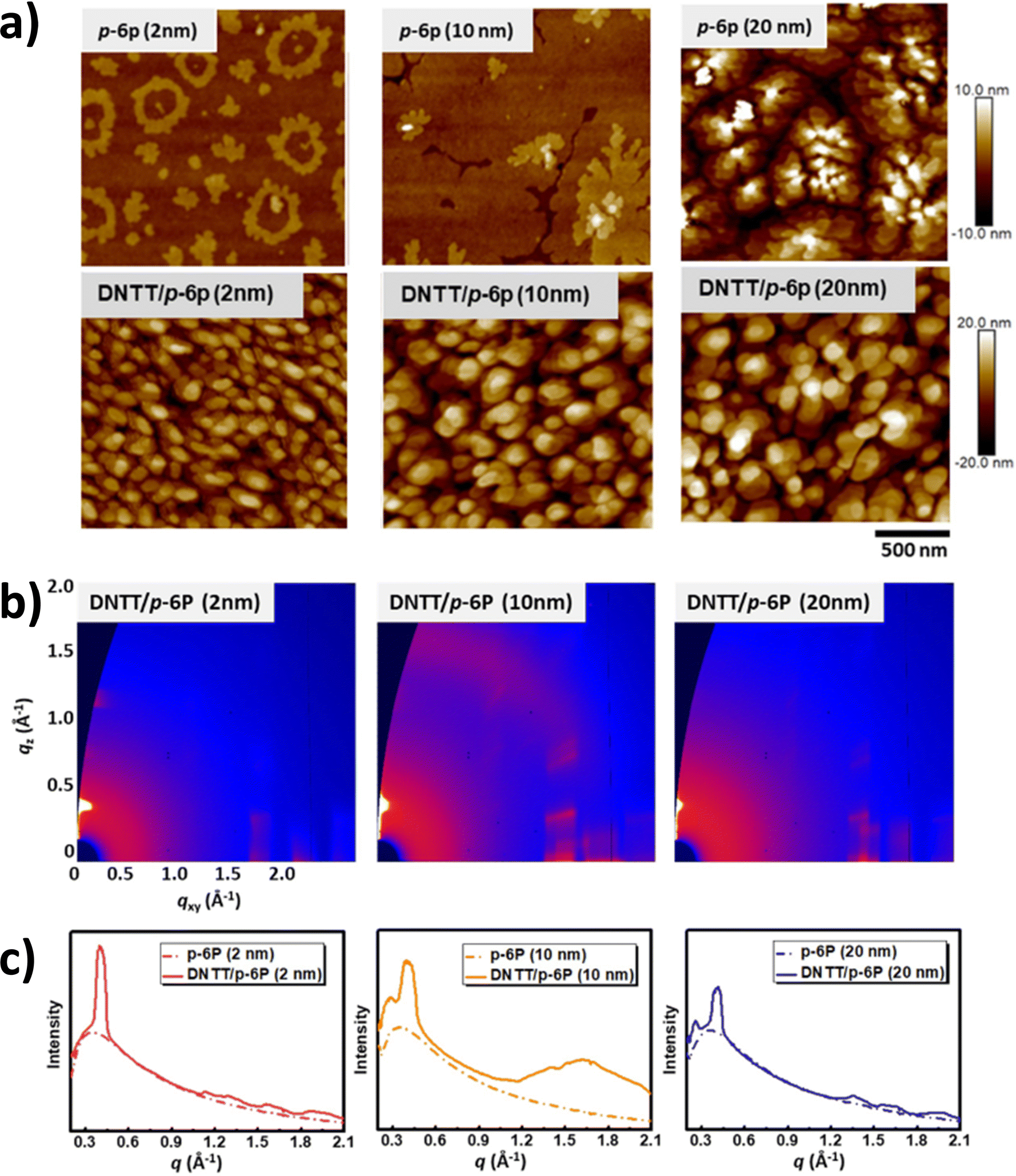 | ||
| Fig. 1 (a) The AFM topographies of the p-6P and DNTT films. (b) The 2D GIXD patterns of the DNTT films on a p-6P template. (c) The 1D GIXD profiles of the p-6P and DNTT films. | ||
The solid-state stacking of the p-6P and DNTT films was characterized using the GIXD technique. The 2D GIXD patterns of the DNTT films on a p-6P template and the p-6P films are presented in Fig. 1b and Fig. S1b–d (ESI†) and the corresponding 1D line cut profiles are displayed in Fig. 1c. As can be seen, the p-6P films presented featureless packing patterns, while the DNTT films exhibited varied structures influenced by the thickness of the p-6P template. Consequently, the d-spacing (Å) and crystallite size (nm) based on (100) diffraction of the DNTT films were (15.5, 8.0), (15.3, 5.8) and (15.2, 8.0) for those grown on a p-6P template of 2 nm, 10 nm, and 20 nm-thick p-6P templates, respectively. In particular, long-range ordering (low-q) was inhibited with a thick p-6P template, while short-range ordering (high-q) was promoted due to an enhanced WEG effect. The DNTT film grown on a 10 nm-thick p-6P template exhibited abnormally enhanced packing in the high-q range compared to those on the 2 nm and 20 nm-thick p-6P templates. This enhancement is attributed to the WEG effect to orient and pack the DNTT molecules; however, short-range ordering was not observed in the DNTT on a 20 nm-thick p-6P template owing to the rough and aggregated p-6P surface, which is unfavorable for WEG. Collectively, the results are in accordance with the variations in the DNTT grain size derived from the AFM topographies. The DNTT molecules were readily self-organized by the bottom-templating p-6P layer due to the π–π orbital overlapping and therefore, this structure is understood to be conducive to the construction of a close contact between the heterojunction for charge transfer and a highly oriented channel to perform charge-carrier transport efficiently.
Optical absorption of fabricated heterojunctions was studied by using the UV-Vis absorption spectra. Heterojunctions exhibit strong broadband optical absorption covering the blue-to-UV region with maximum absorption at ∼450 nm as shown in Fig. S2 (ESI†). To understand the influence of the molecular heterojunction in a bilayer architecture on the dynamic change of photogenerated charges, the time-resolved photoluminescence (TRPL) analysis was performed for DNTT-only and DNTT/p-6P heterojunction thin films upon photoexcitation with 372 nm radiation. The TRPL measurements of emission decays were studied at 465 nm for DNTT-only and the corresponding heterojunctions. The two-dimensional TRPL spectra [Fig. 2a–d] were transformed into 1-D TRPL decay profiles and fitted exponentially [Fig. 2e]. The exciton lifetimes of the studied samples were estimated at 0.267 ns, 0.245 ns, 0.222 ns, and 0.225 ns for DNTT-only, DNTT/p-6P (2 nm), DNTT/p-6P (10 nm), and DNTT/p-6P (20 nm) films, respectively. It is evident that the lifetime of the photogenerated charges is reduced with an increase in the thickness of the molecular template. The charge transfer rate and efficiency of DNTT/p-6P (10 nm) (0.76 ns−1, 16.85%) were estimated to be relatively higher than those of DNTT/p-6P (20 nm) (0.70 ns−1, 15.73%) and DNTT/p-6P (2 nm) (0.34 ns−1, 8.24%). This situation is a result of exciton quenching that should be attributed to rapid and efficient exciton dissociation in the heterojunction and thus would cause enhanced charge-transfer efficiency. TRPL results highlight the potential for fast charge trapping and transfer (exciton quenching) from the photoexcited molecular semiconducting channel to the molecular template electret; this would increase the photonic performance of the corresponding transistor comprising the aforementioned molecular heterojunction.
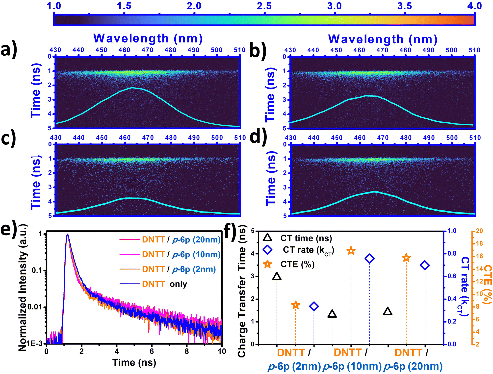 | ||
| Fig. 2 The 2-D time-resolved photoluminescence spectra (TRPL) of the (a) DNTT-only, (b) DNTT/p-6p (2 nm), (c) DNTT/p-6p (10 nm), and (d) DNTT/p-6p (20 nm) heterojunctions. (e) The 1-D TRPL decay profiles of the DNTT-only and heterojunctions. (f) The summary of charge transfer behavior in heterojunctions highlighting the charge transfer rate and efficiency. | ||
To characterize the structure-performance relationship of the heterojunctions for visual memory performance, phototransistor memories derived from heterojunctions were fabricated with the typical bottom-gate/top-contact (BG/TC) architecture. The transfer characteristics of phototransistor memories were tested by sweeping the gate voltage (VGS) between 10 and −60 V under fixed drain voltage (VDS) of −30 V as shown in Fig. S3a, c and e (ESI†). Upon light illumination (450 nm; 30 s duration), the transfer curves were positively shifted, indicating the notable electron trapping behavior of the heterojunctions. The mobility of the heterojunction phototransistors reduced drastically as the thickness of the p-6P template layer increased, as summarized in Table S1 (ESI†). In contrast, the memory window of the heterojunctions increased as the thickness of p-6P increased, highlighting their enhanced charge-trapping capability. The transfer curves returned to the position close to their initial scan under the applied gate voltage (−60 V; 2 s). All the fundamental parameters, such as mobility (μh), threshold voltage (Vth), and ION/IOFF, were estimated from the conventional characterization equation and are summarized in Table S2 (ESI†). Among the molecular heterojunctions studied, DNTT/p-6P (10 nm) delivered the optimal performance with a larger memory window of 14.5 V and ION/IOFF of ∼2 × 10⁵, in good agreement with the exciton quenching estimated by the TRPL study.
The transient photocurrent enhancement of the semiconducting channel is ensured by manipulating the pulse-width of the incident light. This provokes long-lasting visual memory altering from short-term retention for fulfilling optical programing capability. As shown in Fig. S3b, d and f (ESI†) after ≈30 s of light illumination, an initial abrupt increase in the photocurrent was observed. When the illumination was removed, there was a slight decrease. The devices maintained their enhanced photocurrent in the channel, indicating their visual memory characteristics, with a distinct (ION/IOFF) performance for each heterojunction. To manipulate the time dependency of the photocurrent change, the heterojunction memory devices were examined under light stimulation with various pulse widths (1 s, 5 s, 10 s, 20 s, and 30 s). As shown by the temporal IDS curves in Fig. S3 (ESI†), the photocurrent increased as the pulse width increased from 1 s to 30 s. The photocurrent increased sharply upon light illumination of 1 s for both the 2 nm and 10 nm DNTT/p-6P devices. The DNTT/p-6P (10 nm) device showed higher charge retention characteristics and thus a high photocurrent level was maintained for 120 s, demonstrating photoprogramming under a short illumination pulse width (1–10 s). This situation should be attributed to the enhanced charge transfer rate and efficiency of DNTT/p-6P (10 nm) compared to DNTT/p-6P (2 nm). Note that DNTT/p-6P (10 nm) possessed high charge retention stability similar to DNTT/p-6P (20 nm). For photoprogramming operations using pulse widths exceeding 10 s, all the devices studied exhibited high charge retention characteristics. The DNTT/p-6P (10 nm) device had the highest photocurrent enhancement and memory stability for all illumination pulse widths. It is worthwhile to mention that the photoprogramming operation takes place under light illumination at VGS = 0 V (zero-gate operation), which reduces the dependency on the applied voltage.
Considering the realized impact of long light stimulation on the prolonged memory effect, the light/conductivity correlation was studied, using ultranarrow light pulses to modulate the visual neuroplasticity of a perception system. Short-term plasticity and long-term potentiation (STP and LTP) are two forms of fundamental cooperative synaptic facilitation functions of biological synapses responsible for learning, information processing, and recognition capability, in the neuromorphic systems.26–30 These fundamental functions are divided into two categories, based on the change in weight of the synaptic connection between two nodes, describing the temporary enhancement in synaptic weight, which rapidly returns to its original state as STP, whereas stronger stimulus of an event causes long-lasting synaptic weight enhancement, LTP.30–33 Analogically, synaptic weight altering in biological systems corresponds to excitatory postsynaptic current (EPSC) change of the proposed semiconducting channel of the heterojunction architecture via informative light stimulation in the designed optoelectronic artificial synapse [Fig. 3a]. Similar to the memory mode investigated under ≈30 s of light illumination without a gate bias (zero-gate operation), the EPSC of DNTT/p-6P (10 nm) (Fig. S4, ESI†) exhibited the highest exponential enhancement at VDS = −1 V under multiple ultrashort consecutive light pulses compared to those of the other heterojunctions with various p-6P thicknesses. The DNTT/p-6P (10 nm) synapse was examined to mimic fundamental visual neuroplasticity to achieve STP, heralded by its most common form, namely paired-pulse facilitation (PPF), demonstrating the greater enhancement in synaptic weight in favor of the second spike than that of the first stimulation under a pair of successive light pulses. As seen in Fig. 3b, EPSC was enhanced after the second of two successive pulses (wavelength 450 nm; width 50 ms; interval 50 ms), exhibiting STP with an extremely high PPF ratio of 206%. As with its biological counterparts, the PPF ratio reduced exponentially [Fig. 3c] as Δt increased from 50 ms to 2 s, which is in good agreement with reported photosynapses. When the time interval exceeded 800 ms, the PPF ratio of the proposed bilayer device stabilized, with a high PPF ratio of over 150% for this interval, outperforming other reported systems. Such a high PPF ratio provides clear evidence originating from the photo-excitation of a well-packed DNTT molecule framework under 450 nm and favorable deep traps provided by the p-6P molecular electret template owing to the favorable HOMO/LUMO levels.
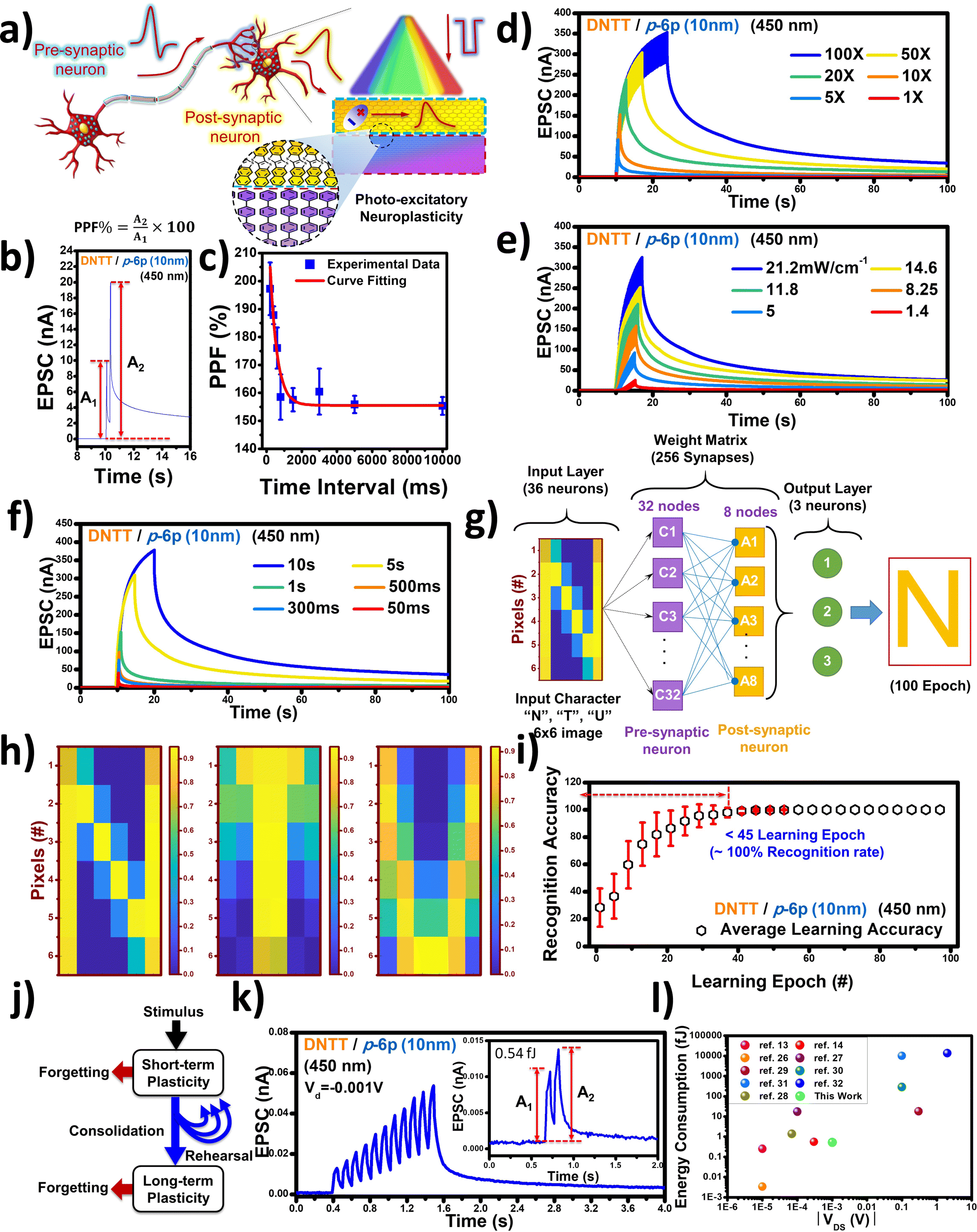 | ||
| Fig. 3 (a) Schematic illustration of the analogy between fabricated heterojunction photosynapses and the biological one. (b) The transient EPSC profile of the DNTT/p-6p (10 nm) device emulating the PPF behavior under light illumination (width: 50 ms; interval: 200 ms) at VDS = −1 V. (c) The variation of PFF ratios as a function of pulse interval spanning in the range of 50 ms to 10 s. (d) SNDP, (e) SNDP, and (f) STDP of the DNTT/p-6p (10 nm) photosynapse under 450 light illumination at VDS = −1 V. (g) Schematic illustration of the single-layer perception artificial NN consisting of 32 pre-synaptic and 8 post-synaptic neurons. (h) Artificial neural network of 6 × 6 array images for the pattern recognition process of letters “N, T, U”. (i) Pattern recognition accuracy of the proposed artificial neural network. (j) Rehearsal-learning process in the human brain. (k) The EPSC change after consecutive light pulses with an operating voltage of −0.001 V. The inset shows the EPSC excited by consecutive photonic pulses at an ultralow voltage. (l) Comparison of the energy consumption of this work and those of the previously published organic artificial photonic synapses. | ||
In the nervous system, a stronger stimulus of an event, provoking LTP, strengthens the connection between pre-synaptic and post-synaptic neurons, consolidating long-lasting permanent memory retention in the human brain.34,35 Accordingly, the transition from STP to LTP in visual neuroplasticity can be provoked by altering the light stimulation parameters such as the number of pulses, pulse intensity, and pulse width.36,37 One common form of LTP is the spike-number-dependent synaptic plasticity (SNDP), which is stimulated by applying light pulses ranging from 1 to 100 pulses (450 nm; 21.2 mW cm−2; 50 ms) to the device, consolidating the transition and prolonging the long-term memory functionality, as illustrated in Fig. 3d. The spike-intensity-dependent plasticity (SIDP) and spike-timing-dependent plasticity (STDP) are also fundamental processes of biological synapses in neural networks. The performance of the proposed heterojunction electret with a semiconducting molecular channel (DNTT/p-6P (10 nm)) was demonstrated with high reproducibility by the variations in light intensity and pulse width, exhibiting the transition from short-term plasticity to long-term potentiation as presented in Fig. 3e and f. As illustrated in Fig. 3d–f, the origin of this transition relies on the hysteresis in the EPSC preventing the device from returning to its original state during the 100 s reading period; this is due to the charge accumulation/trapping in the molecular heterojunction increasing the EPSC current in the synaptic channel. The fitted time constants of the forgetting curves as a result of SNDP, SIDP, and STDP functionalities [Fig. 3d–f] are summarized in Table S3 (ESI†), indicating prolonged hysteresis as the applied pulse number, intensity, and pulse width increased, which refers to repeated, stronger, and prolonged stimuli of an event, as happens in biological synapses. To compare the uniformity of the synaptic response, the results of 10 different cells of three different batches are summarized in Fig. S3 (ESI†). The results highlight negligible difference in the dark conductivity, which may have resulted from the fabrication condition in studied pixels of different samples. The statistical analysis of the EPSC change under a single light pulse (450 nm; width: 50 ms) exhibits a uniform enhancement (A1) for each cell from the studied heterojunction photosynapses, as summarized in Fig. S3 (ESI†). The distribution of EPSC ratio after the fiftieth pulse to the first pulse (A50/A1) was exhibited in a similar level with a narrow deviation, highlighting the uniformity of cell-to-cell synaptic performance in the heterojunction photosynapse. These interesting results indicate the emulation of visual neuroplasticity facilitating optical memory and learning functionalities in a designed device.
Neural networks (NNs) are computing systems inspired by the human brain consisting of an interconnected nervous network through synapses and neurons as building blocks in the nervous systems of living organisms responsible for transferring input information, to perform various fundamental operations including power efficient sensing, perception, processing, learning, memory, and recognition by data transmission.38 To mimic the visual pattern recognition and memory training/learning capacity of the proposed NN, a 6 × 6 array of devices was fabricated using the same molecular heterojunction architecture of DNTT/p-6P (10 nm). The scheme of synaptic connections between pre-synaptic and post-synaptic neurons is shown in Fig. 3g. For each training epoch, synaptic weight changes (that is, EPSC enhancement of each pixel) were recorded for 50 consecutive light pulse stimulations (wavelength 450 nm; intensity 21.2 mW cm−2; width 50 ms; and interval 50 ms), which demonstrates the visual memory update characteristics of the neural network. The scheme represents a single-layer perception of an NN consisting of 32 pre-synaptic and 8 post-synaptic neurons with a concomitant 256 synaptic connections in a proposed optical NN, where the synaptic connections were carried out depending on the optical-sensing process using a vector–matrix multiplication method in mathematical simulation software. A series of letters, ‘N’, ‘T’, and ‘U’, was introduced with a data set of input font images custom-defined to train and test the recognition accuracy of the output layer consisting of 3 neurons. After a training and recognition process of 100 iterative simulations, various letter patterns of input images were learned by the system without supervision, as shown in Fig. 3h. Fig. 3i summarizes the accuracy of recognition of trained letters after a training epoch of 100 iterations, depending on EPSC values of the pixels displayed by the color bar [Fig. 3h]. The output of the trained neurons demonstrates a high recognition rate, up to 100%, in a proposed two-layer NN after a learning epoch of approximately 45 iterations. The high recognition rate achieved by the 6 × 6 photosynapse array-based NN model should be attributed to the large input gaps between pixels and defined 50-different primary patterns of fonts, similar to the achieved high recognition rate in the literature.39 In conclusion, the simulated artificial NN system mimics the pattern learning and visual memory of human brain activities via repetitive visual training sessions, altered by variations in the synaptic weight change (EPSC) under ultrashort consecutive light stimulation, as shown schematically in Fig. 3i. These results highlight the feasibility of employing the heterojunction phototransistors in real-time artificial visual devices for high-speed image processing/memory systems. More importantly, the simplified architecture and compatible fabrication process with standard techniques hold great promise for applications of molecular heterojunctions in large phototransistor arrays with high-density, photogate configurability and efficient in-sensor image processing capability for future biomimetic visual systems.
In contrast to conventional voltage-driven memory technologies,40–42 our optoelectronic synapse comprising a molecular heterojunction architecture can be operated even under an ultralow operating VDS of −0.001 V and ultrashort light stimulation of 50 ms. The EPSC enhancement was observed after each consecutive light pulse (wavelength 450 nm; intensity 21.2 mW cm−2; pulse width 50 ms), demonstrating a transition from STP-to-LTP, according to rehearsal learning, as shown in Fig. 3j. The PPF ratio for the optoelectronic synapse was determined as 133%, even at this extremely low operating voltage and light intensity, as shown in the inset of Fig. 3k. The energy consumption per synaptic event was estimated as 0.54 fJ at a VDS of −0.001 V. Such a low energy consumption outperforms those of the conventional memory systems and competes with those of the published inorganic composite and organic polymer optoelectronic synapses, as presented in Fig. 3l and Table S4 (ESI†) and it is also lowers than the consumption per synaptic event of the human brain.43
Conclusions
In conclusion, we demonstrated the effect of heterojunction morphology and growth via molecular templates, to tailor the charge transport and high-performance visual memory/synapse characteristics of the derived devices. The morphology and optical properties of the heterojunctions were systematically characterized. p-6P showed promising potential as an effective molecular template for anisotropic control via weak epitaxial growth of a DNTT semiconducting channel and thus for manipulating the charge transport/trapping. Thanks to the favorable LUMO/HOMO levels (−1.8/−5.6 eV) and high optical band gap (3.8 eV), a fabricated phototransistor memory device with optimized p-6P thickness exhibited a high ION/IOFF ratio (∼2 × 10⁵) with a large memory window (14.5 V) and memory retention discriminability outperforming its counterparts with diverse morphology owing to the molecular template thickness. The long-lasting visual memory was demonstrated by variation in the pulse-width of the incident light and has potential for long-term data retention capability. Finally, the heterojunction with the best performance was investigated under ultrashort light stimulation to explore its visual synaptic functionalities, with a high pair-pulse index of ∼206% to mimic sensing, computing, and memory functions by controlling the pulse number, light intensity and pulse-width similar to biological counterparts. The proposed artificial NNs possess high pattern recognition of various letter patterns of input images, mimicking the neuroplasticity of human brain activities via repetitive visual training sessions for rehearsal learning. The energy consumption per synaptic event of the proposed device was estimated at 0.54 fJ under an ultralow operation voltage (−0.001 V) and zero-gate operation, exhibiting superior performance compared to previously published composite optoelectronic synapses. The experimental results suggest that the emulation of human-like memory and learning functionalities in composite nanostructures can be constructed by a facile molecular template approach. This study provides a guide to the design of molecular heterojunctions to tailor high performance photonic memory and synapses for neuromorphic computing.Conflicts of interest
There are no conflicts to declare.Acknowledgements
The authors acknowledge the Ministry of Education's Higher Education Sprout Project under the Featured Area Research Center Program (111L9006) and the National Science and Technology Council in Taiwan (NSTC 111-2634-F-002-016) for financial support.Notes and references
- Y. Zhai, J.-Q. Yang, Y. Zhou, J.-Y. Mao, Y. Ren, V. A. L. Roy and S.-T. Han, Mater. Horiz., 2018, 5, 641–654 RSC.
- Y. Yu, Q. Ma, H. Ling, W. Li, R. Ju, L. Bian, N. Shi, Y. Qian, M. Yi, L. Xie and W. Huang, Adv. Funct. Mater., 2019, 29, 1904602 CrossRef CAS.
- Y.-C. Lin, W.-C. Yang, Y.-C. Chiang and W.-C. Chen, Small Sci., 2022, 2, 2100109 CrossRef CAS.
- S. Dai, Y. Zhao, Y. Wang, J. Zhang, L. Fang, S. Jin, Y. Shao and J. Huang, Adv. Funct. Mater., 2019, 29, 1903700 CrossRef CAS.
- J. Zhang, S. Dai, Y. Zhao, J. Zhang and J. Huang, Adv. Intell. Syst., 2020, 2, 1900136 CrossRef.
- S. Song, J. Kim, S. M. Kwon, J. W. Jo, S. K. Park and Y. H. Kim, Adv. Intell. Syst., 2020, 3, 2000119 CrossRef.
- C. Wang, X. Zhang and W. Hu, Chem. Soc. Rev., 2020, 49, 653–670 RSC.
- C. Xie, C.-K. Liu, H.-L. Loi and F. Yan, Adv. Funct. Mater., 2020, 30, 1903907 CrossRef CAS.
- H. Ren, J.-D. Chen, Y.-Q. Li and J.-X. Tang, Adv. Sci., 2021, 8, 2002418 CrossRef CAS PubMed.
- D. Hao, J. Zhang, S. Dai, J. Zhang and J. Huang, ACS Appl. Mater. Interfaces, 2020, 12, 39487–39495 CrossRef CAS PubMed.
- E. Ercan, Y. C. Lin, W. C. Yang and W. C. Chen, Adv. Funct. Mater., 2022, 32, 2107925 CrossRef CAS.
- J.-Y. Chen, D.-L. Yang, F.-C. Jhuang, Y.-H. Fang, J.-S. Benas, F.-C. Liang and C.-C. Kuo, Adv. Funct. Mater., 2021, 31, 2105911 CrossRef CAS.
- B. Yang, Y. Lu, D. Jiang, Z. Li, Y. Zeng, S. Zhang, Y. Ye, Z. Liu, Q. Ou, Y. Wang, S. Dai, Y. Yi and J. Huang, Adv. Mater., 2020, 32, 2001227 CrossRef CAS PubMed.
- W.-C. Yang, Y.-C. Lin, S. Inagaki, H. Shimizu, E. Ercan, L.-C. Hsu, C.-C. Chueh, T. Higashihara and W.-C. Chen, Adv. Sci., 2022, 9, 2105190 CrossRef CAS PubMed.
- X. Wang, Y. Lu, J. Zhang, S. Zhang, T. Chen, Q. Ou and J. Huang, Small, 2021, 17, 2005491 CrossRef CAS PubMed.
- C.-H. Ho, Y.-C. Lin, W.-C. Yang, E. Ercan, Y.-C. Chiang, B.-H. Lin, C.-C. Kuo and W.-C. Chen, ACS Appl. Mater. Interfaces, 2022, 14, 15468–15477 CrossRef CAS PubMed.
- B. Yang, Y. Wang, L. Li, J. Zhang, J. Wang, H. Jiao, D. Hao, P. Guo, S. Zeng, Z. Hua and J. Huang, Adv. Funct. Mater., 2021, 31, 2103787 CrossRef CAS.
- Y. Chen, Y. Chu, X. Wu, W. Ou-Yang and J. Huang, Adv. Mater., 2017, 29, 1704062 CrossRef PubMed.
- S. Dai, X. Wu, D. Liu, Y. Chu, K. Wang, B. Yang and J. Huang, ACS Appl. Mater. Interfaces, 2018, 10, 21472–21480 CrossRef CAS PubMed.
- Q.-X. Li, T.-Y. Wang, X.-L. Wang, L. Chen, H. Zhu, X.-H. Wu, Q.-Q. Sun and D. W. Zhang, Nanoscale, 2020, 12, 23150–23158 RSC.
- Y. Chu, X. Wu, J. Lu, D. Liu, J. Du, G. Zhang and J. Huang, Adv. Sci., 2016, 3, 1500435 CrossRef PubMed.
- J. Guo, D. Liu, W. La, B. Yu, H. Tian, F. Zhu and D. Yan, Org. Electron., 2021, 93, 106170 CrossRef CAS.
- S. Oh, G. Choi, J. Seo, S. Li, T. Hwang, E. Park and H. S. Lee, Adv. Electron. Mater., 2022, 8, 2101115 CrossRef CAS.
- C. Qian, J. Sun, L.-A. Kong, Y. Fu, Y. Chen, J. Wang, S. Wang, H. Xie, H. Huang, J. Yang and Y. Gao, ACS Photonics, 2017, 4, 2573–2579 CrossRef CAS.
- C. Qian, S. Oh, Y. Choi, J.-H. Kim, J. Sun, H. Huang, J. Yang, Y. Gao, J.-H. Park and J. H. Cho, Nano Energy, 2019, 66, 104095 CrossRef CAS.
- B. Yang, Y. Wang, Z. Hua, J. Zhang, L. Li, D. Hao, P. Guo, L. Xiong and J. Huang, Chem. Commun., 2021, 57, 8300–8303 RSC.
- Q. Ou, B. Yang, J. Zhang, D. Liu, T. Chen, X. Wang, D. Hao, Y. Lu and J. Huang, Small, 2021, 17, 2007241 CrossRef CAS PubMed.
- X. Wang, Y. Lu, J. Zhang, S. Zhang, T. Chen, Q. Ou and J. Huang, Small, 2021, 17, 2005491 CrossRef CAS PubMed.
- H.-L. Park, H. Kim, D. Lim, H. Zhou, Y.-H. Kim, Y. Lee, S. Park and T.-W. Lee, Adv. Mater., 2020, 32, 1906899 CrossRef CAS PubMed.
- J. Zhang, Q. Shi, R. Wang, X. Zhang, L. Li, J. Zhang, L. Tian, L. Xiong and J. Huang, InfoMat, 2021, 3, 904–916 CrossRef CAS.
- S. Wang, C. Chen, Z. Yu, Y. He, X. Chen, Q. Wan, Y. Shi, D. W. Zhang, H. Zhou, X. Wang and P. Zhou, Adv. Mater., 2019, 31, 1806227 CrossRef PubMed.
- C. Yang, J. Qian, S. Jiang, H. Wang, Q. Wang, Q. Wan, P. K. L. Chan, Y. Shi and Y. Li, Adv. Opt. Mater., 2020, 8, 2000153 CrossRef CAS.
- E. Ercan, Y. C. Lin, Y. Sakai-Otsuka, R. Borsali and W. C. Chen, Adv. Opt. Mater., 2022, 2201240 CrossRef CAS.
- X. Liu, F. Wang, J. Su, Y. Zhou and S. Ramakrishna, Adv. Funct. Mater., 2022, 32, 2113050 CrossRef CAS.
- X. Chen, B. Chen, B. Jiang, T. Gao, G. Shang, S.-T. Han, C.-C. Kuo, V. A. L. Roy and Y. Zhou, Adv. Funct. Mater., 2023, 33, 2208807 CrossRef CAS.
- E. Ercan, L. C. Hsu, Y. C. Lin, B. H. Lin and W. C. Chen, ACS Appl. Polym. Mater., 2023, 5, 463–475 CrossRef CAS.
- W.-C. Yang, E. Ercan, Y.-C. Lin, W.-C. Chen, Y. Watanabe, K. Nakabayashi, B.-H. Lin, C.-T. Lo, H. Mori and W.-C. Chen, Adv. Opt. Mater., 2022, 2202110 Search PubMed.
- S. W. Cho, S. M. Kwon, Y. H. Kim and S. K. Park, Adv. Intell. Syst., 2021, 3, 2000162 CrossRef.
- C. Jo, J. Kim, J. Y. Kwak, S. M. Kwon, J. B. Park, J. Kim, G.-S. Park, M.-G. Kim, Y.-H. Kim and S. K. Park, Adv. Mater., 2022, 34, 2108979 CrossRef CAS PubMed.
- D. Chatterjee, U. A. Jadhav, B. H. Javaregowda, T. D. Dongale, P. S. Patil and P. P. Wadgaonkar, Eur. Polym. J., 2021, 147, 110327 CrossRef CAS.
- T. S. Bhat, C. C. Revadekar, S. S. Patil, T. D. Dongale, D. K. Kim and P. S. Patil, J. Mater. Sci. Mater., 2020, 31, 10919–10929 CrossRef CAS.
- S. T. Killedar, N. A. Ahir, P. J. Morankar, A. P. Tiwari, P. B. Patil, T. D. Dongale and D. K. Kim, Opt. Mater., 2020, 109, 110333 CrossRef CAS.
- W. Xu, S.-Y. Min, H. Hwang and T.-W. Lee, Sci. Adv., 2016, 2, e1501326 CrossRef PubMed.
Footnote |
| † Electronic supplementary information (ESI) available. See DOI: https://doi.org/10.1039/d2nh00597b |
| This journal is © The Royal Society of Chemistry 2023 |