
 Open Access Article
 This Open Access Article is licensed under a Creative Commons Attribution-Non Commercial 3.0 Unported Licence
Solution-based in situ deposition of Sb2S3 from a single source precursor for resistive random-access memory devices†
Sayali Shrishail
Harke
 a,
Tongjun
Zhang
b,
Ruomeng
Huang
b and
Chitra
Gurnani
*a
a,
Tongjun
Zhang
b,
Ruomeng
Huang
b and
Chitra
Gurnani
*a
aEcole Centrale School of Engineering, Mahindra University (MU), Hyderabad, India. E-mail: chitra.gurnani@mahindrauniversity.edu.in
bSchool of Electronics and Computer Science, University of Southampton, Southampton, UK
First published on 16th August 2023
Abstract
A one-step, simple, scalable, reproducible, low-temperature, and in situ solvothermal deposition method has been established for the growth of Sb2S3 on FTO using [Sb{S2P{O(Pr)2}3] as a single source precursor without a binding agent. XRD, Raman, SAED, and HRTEM results revealed the crystalline orthorhombic stibnite phase. The sheaf-like Sb2S3 exhibited a band gap energy of 1.72 eV. The Sb2S3 film is uniform and well-adhered and is further developed as a novel resistive random-access memory material. The Ag/Sb2S3/FTO memristive device demonstrated low operating voltage and the performance of the device over multiple cycles revealed dependable bipolar resistive switching behaviour and an ON/OFF ratio of ca. 10.
1. Introduction
A promising aspect of new non-volatile memory technologies is their predicted capacity gains, non-volatility, and lack of idle energy. The most promising alternative is resistive random access memory (RRAM), which is based on resistive switching (RS). RRAM devices have recently undergone rapid development, due to their unique qualities, including consumption of low power, fast switching rates, superior scalability, and increased data endurance and retention capabilities.1–10 Developing highly effective and low-powered devices is important for RRAM since it must satisfy high technological needs with extensive integration. However, it is difficult to achieve an effective performance of the device within a single device with low switching voltage, operating current, a better ON/OFF ratio, and dependable switching behaviour.11 Resistive switching has been detected in oxides,12 chalcogenides,13 and organic,14 as well as organic–inorganic hybrid materials.15,16Metal oxides (such as WO3, SiO2, ZrO2, TiO2, and CuO) and germanium chalcogenides (GexSx or GexSex, and GexTey) exhibit attractive switching characteristics.17–23 There is a constant need to explore novel memristive materials. Sb2S3 is an efficient light-absorbing material and has been reported to exhibit light induced transformation of resistive switching polarity in Sb2S3 based organic–inorganic hybrid devices. Moreover, Sb2S3 possesses a high absorption coefficient, suitable bandgap (1.7 eV), earth-abundancy, high stability, reduced toxicity,24–30 high resistance and low carrier concentration.31,32 To our knowledge, there have been only two reports, where Sb2S3 was used for memristor applications.33,34 Consequently, there is a lot of interest in the development of efficient and novel routes to synthesize Sb2S3.
The majority of the published investigations on the deposition of Sb2S3 emphasized on the utilization of dual-source precursors (DSPs), and very few studies exploited the usage of single-source precursor (SSP) complexes. SSPs can increase atom efficiency and simplicity of handling while enabling precursor design to control characteristics like stoichiometry and morphology.35 The SSP methods offer mildness, safety, and a more streamlined production process compared to the usage of DSP methods, which necessitates strict control over stoichiometry.36 Only high temperature routes such as aerosol-assisted chemical vapor deposition (AACVD),37,38 and the electrodeposition method34 have been explored for Sb2S3; however, low temperature and solution processible routes using SSPs for deposition of Sb2S3 have not been explored so far. Solvothermal deposition is simple in operation, a low-temperature deposition process, controls the overall growth rate, doesn’t involve any complicated devices, has low production cost, and has the prospect of being suitable for large-scale industrial production. Sb2S3 (stibnite) powder has been generated via a solvothermal method39,40 with high boiling solvent oleylamine and via a refluxing route.41 Nonetheless, in situ solvothermal deposition of Sb2S3 thin films from SSPs without any binding agents and additional step of annealing has lingered unexplored. Dithiophosphate (DTP) complexes exhibit diverse coordination patterns.42 They are well defined molecular species and contain performed M–S bonds that decompose when heated, either in a vapor or solution phase, with the easy loss of organics and creation of low-dimensional metal sulfides as a result. The incredible adaptability of DTP complexes as SSPs is due to their simplicity in synthesis and handling, long metal complex shelf lives, and relative stability. To date, there has been no report on the deposition of Sb2S3 films using SSPs from DTP by an in situ solvothermal process. Consequently, there is immense potential to explore novel routes for mass manufacturing of Sb2S3 films towards memristors.
In this study, we report a one-step, simple, scalable, reproducible, and in situ solvothermal deposition for the growth of Sb2S3 on a substrate. The deposition of Sb2S3 was performed at a very low deposition temperature by using SSP [Sb{S2P{O(Pr)2}3] without a binding agent. The deposited film is uniform and well-adhered, and further utilized as a resistive random-access memory device, which demonstrated typical bipolar resistive switching behaviour. Remarkably, the Ag/Sb2S3/FTO memristive device exhibited characteristics of low operating voltage, stability over multiple cycles and an ON/OFF ratio of ca. 10.
2. Experimental
2.1 Materials
SbCl3 and P2S5 were procured from Sigma Aldrich and utilized as received. Propan-1-ol (Pr-99%) (b.p. 97 °C), and toluene (99.5%) (b.p. 110.6 °C) were bought from SDFCL and FINAR, respectively. Triethylamine (99%), n-hexane (99%), dichloromethane (DCM) (99.5%), ethanol (99.9%), and ethylene glycol (99.5%) were purchased from SDFCL, SRL, FINAR, Analytical reagent, and Fischer Scientific, respectively, and used as received.2.2 Preparation of precursor and characterization
All the reactions were performed in Schlenk and vacuum lines. n-Hexane, toluene, propan-1-ol, dichloromethane and triethylamine were freshly distilled prior to use. Ethanol and ethylene glycol were used as received. On a Nicolet iS5 Thermo Scientific equipment, IR spectra were captured using KBr discs in the wavelength range of 4000–400 cm−1. On a Bruker Avance Neo 500 MHz NMR spectrometer, {1H} NMR and 31P{1H} NMR spectra were collected in CDCl3 solution at room temperature in SAIF, Punjab University, Chandigarh.![[double bond, length as m-dash]](https://www.rsc.org/images/entities/char_e001.gif) S) and 555(s), ν(P–S).
S) and 555(s), ν(P–S).
![[thin space (1/6-em)]](https://www.rsc.org/images/entities/char_2009.gif) :1 molar ratio and continuously stirred at room temperature for 1 h. Filtration under anhydrous conditions was performed to extract the triethylamine chloride precipitate, and excess solvent has been eliminated from the filtrate in vacuo to produce a light pale yellow precipitate. To produce yellow needle-shaped crystals, the solution was crystallized by adding DCM and n-hexane and then refrigerated for two days. Yield: 0.7 g, 92.7%; {1H} NMR (CDCl3, 298 K, δ ppm): 1.3 (m, [6H], –CH3), 3.08 (m, [4H], –CH2CH3), 4.82 (m, [4H], –CH2); 31P{1H} (CDCl3, 298 K, δ ppm): 87.10(s); IR (KBr) (cm−1): 1180(s), ν{(P)–O–C}; 788(s), ν{P–O–(C)}; 665(s), ν(PS); 547(s), ν(P–S).
:1 molar ratio and continuously stirred at room temperature for 1 h. Filtration under anhydrous conditions was performed to extract the triethylamine chloride precipitate, and excess solvent has been eliminated from the filtrate in vacuo to produce a light pale yellow precipitate. To produce yellow needle-shaped crystals, the solution was crystallized by adding DCM and n-hexane and then refrigerated for two days. Yield: 0.7 g, 92.7%; {1H} NMR (CDCl3, 298 K, δ ppm): 1.3 (m, [6H], –CH3), 3.08 (m, [4H], –CH2CH3), 4.82 (m, [4H], –CH2); 31P{1H} (CDCl3, 298 K, δ ppm): 87.10(s); IR (KBr) (cm−1): 1180(s), ν{(P)–O–C}; 788(s), ν{P–O–(C)}; 665(s), ν(PS); 547(s), ν(P–S).
2.3 In situ solvothermal deposition of Sb2S3 films from [Sb{S2P{O(Pr)2}3]
A dispersion of [Sb{S2P{O(Pr)2}3] (1 g) in 20 mL of ethylene glycol was prepared with continuous stirring for 1 h. Fluorine-doped tin oxide (FTO) was cleaned in an ultrasonicator using deionized water, isopropanol, and acetone prior to film deposition. The aforementioned solution was then shifted to a 25 ml Teflon-lined stainless steel autoclave, in which FTO, a conducting substrate, was submerged horizontally. The autoclave was sealed and maintained at 180 °C for 24 hours. Furthermore, the autoclave was allowed to cool down to room temperature. Subsequently, the film was removed and vacuum-dried for 24 hours. A black film was acquired. Fig. 1 depicts the design of the in situ solvothermal process for fabricating Sb2S3 films.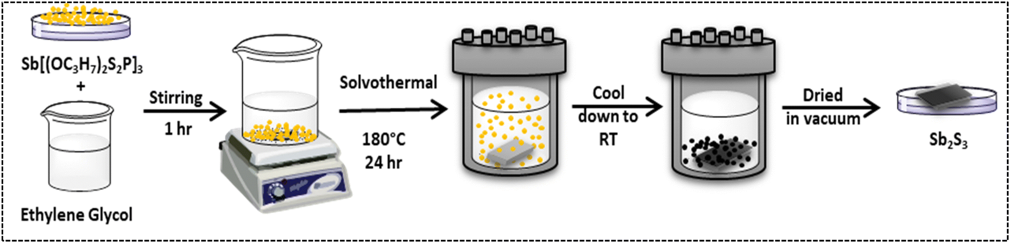 | ||
| Fig. 1 Schematic representation of deposition of the Sb2S3 film by the in situ solvothermal process. | ||
2.4 Sb2S3 film characterization
A Rigaku SmartLab diffractometer (Cu-K) was used for X-ray diffraction (XRD). The samples were scanned between 10° and 80°, with 40 kV and 50 mA supplied as the voltage and current, respectively. The generated pattern was phase-corresponded to card number 042-1393 (stibnite) in the Inorganic Crystal Structure Database (ICDD) using the PDF-2 2021 software package. OXFORD Instruments INCA Wave was used for energy-dispersive X-ray (EDX) spectroscopy and scanning electron microscopy (SEM) investigation. A Gemini/ZEISS ULTRA 55 was used for SEM, with a working distance of 5–8 mm between a sample and the pole piece as well as an acceleration voltage of 5 keV. EDX was implemented with INCA-Point & ID Software and a 20 keV acceleration voltage. Raman spectroscopy was performed with the help of a Horiba Scientific Instruments along with a microscope and a 633 nm laser diode. Spectra were obtained by applying 25% laser power. The Multipurpose Analytical S/TEM JEM-F200 “F2” from Japan was operated at 200 kV to provide images for high-resolution transmission electron microscopy (HR-TEM), and selected area diffraction (SAED) patterns were obtained. A Shimadzu, UV-2600i, Japan spectrophotometer was used for the optical characterization of the Sb2S3 films.2.5 Fabrication of the Sb2S3 electrical device and characterization
As-deposited Sb2S3 serves as a resistive switching layer in the device. A silver (Ag) top with a thickness of 200 nm was patterned on the surface of the Sb2S3 layer by thermal evaporation. The bottom and top contacts were the FTO substrate and Ag electrode, respectively. A probe attached to a Keysight (B1500) system was used for assessing the electrical properties at room temperature and ambient pressure. Throughout all measurements, the top contact received the voltage while the bottom contact was connected to ground.3. Results and discussion
3.1 Precursor preparation and spectroscopic studies
S) or ν(P–S)asym and ν(P–S) or ν(P–S)sym stretching vibrations were shifted to a lower wavenumber by 30–40 cm−1 upon comparison with the [Et3NH][(OC3H7)2S2P], which is consistent with the coordination of the ligand to the central Sb-atom (Fig. S4, ESI†).
The {1H} NMR spectrum for the [Sb{S2P{O(Pr)2}3] compound (Fig. S5, ESI†) was compared with that of the corresponding [Et3NH][(OC3H7)2S2P]. In the complex, the –CH3 perceived as multiplets in the region of 1.3–4.82 ppm, display coordination shift of approximately 0.4 ppm associated with those in the corresponding salts. The 31P{1H} NMR spectrum of the complex demonstrates a sharp singlet at 87 ppm indicating dithiophosphate group coordination to the antimony centre in the molecule43–45 (Fig. S6, ESI†). This revealed the equivalent nature of phosphorous nuclei and in solution, there existed just one form of phosphorus. The 31P{1H} NMR chemical shift for this complex was 23 ppm upfield from that of the equivalent [Et3NH][(OC3H7)2S2P], which represents the anisobidentate nature46 of dithiophosphate moieties. Glidewell concluded that signals in the range of 82–101 ppm represent complexes with bidentate ligands whereas monodentate ligands were found in those with signals smaller than 82 ppm after evaluating the proton decoupled 31P{1H} NMR chemical shifts of a variety of metal dialkyl dithiophosphate.47 This shows that bidentate coordination of the dithiophosphate with antimony is rather robust in solution.
3.2 Deposition of Sb2S3 films via the in situ solvothermal process
Fig. 1 depicts the schematic representation of the experimental setup. Here, the in situ solvothermal process serve as an alternative low temperature solution-processed method. The deposition of Sb2S3 by immersing FTO in solution of [Sb{S2P{O(Pr)2}3] and ethylene glycol allow formation of the film under a low temperature thermal process and further avoiding any additional step of annealing. The compatibility of the precursor with an appropriate solvent to avoid further oxidation is essential, hence the choice of a solvent plays the key role in addition to variation in the various deposition parameters. In hydrothermal or solvothermal synthesis, ethylene glycol is frequently used as a solvent.48 It is both an organic biocompatible solvent and a hydrophilic liquid that is water soluble. The deposited Sb2S3 film is pure, uniform and well-adhered without the addition of any binding agent. The optimization of the deposition parameter, for example, reaction time (12 h, 18 h and 24 h) was investigated at a lower temperature (180 °C). It was observed that, Sb2S3 films deposited at low reaction times, 12 h and 18 h, ensued the phosphorous impurity; while the film that was deposited at 24 h enhanced the quality of the film yielding pure Sb2S3. After the reaction, the black film was obtained at a lower temperature (180 °C).3.3 Sb2S3 film characterization
The deposited black Sb2S3 film is reproducible and highly stable in air and moisture. The data were successfully interpreted using several characterisation techniques such as XRD, Raman spectroscopy, SEM, and UV-Vis spectroscopy.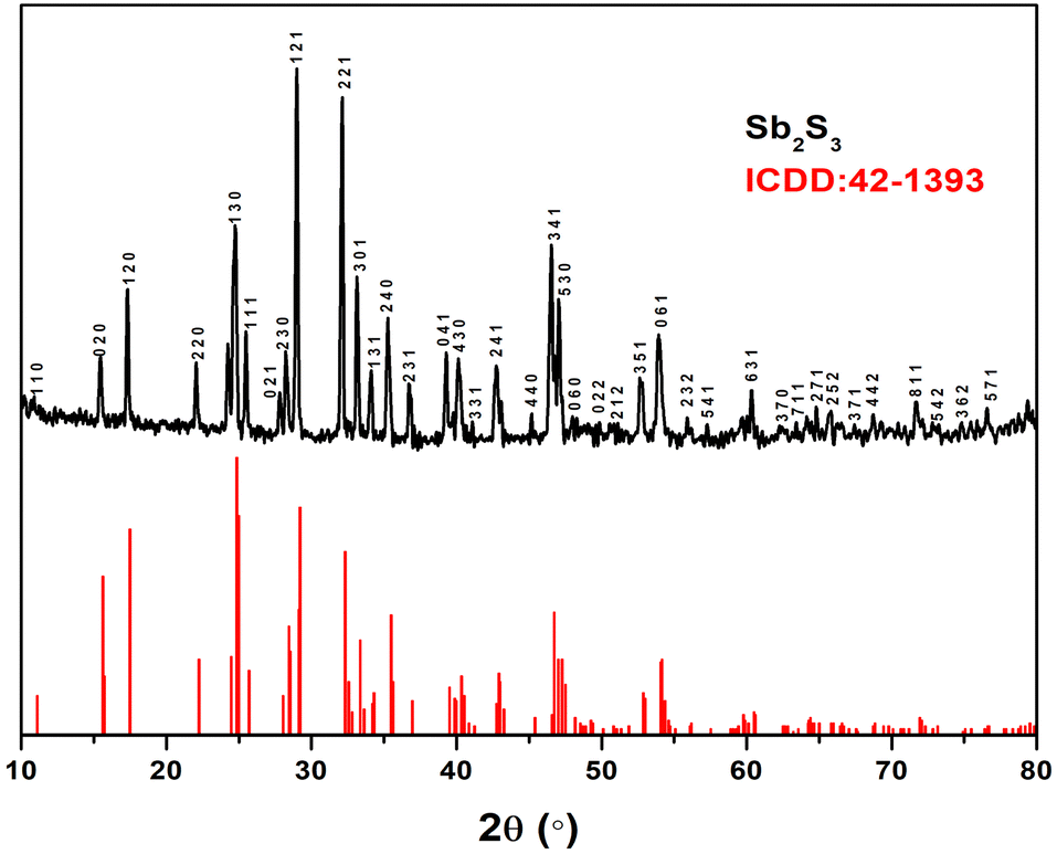 | ||
| Fig. 2 XRD spectrum of the as-deposited Sb2S3 on FTO using Sb[(OC3H7)2S2P]3 as SSP. | ||
The Debye–Scherrer equation (eqn (1)) was applied to XRD data to determine the crystallite diameter (Dc) of Sb2S3, which was found to be 43.62 nm.
| Dc = Kλ/βcosθ | (1) |
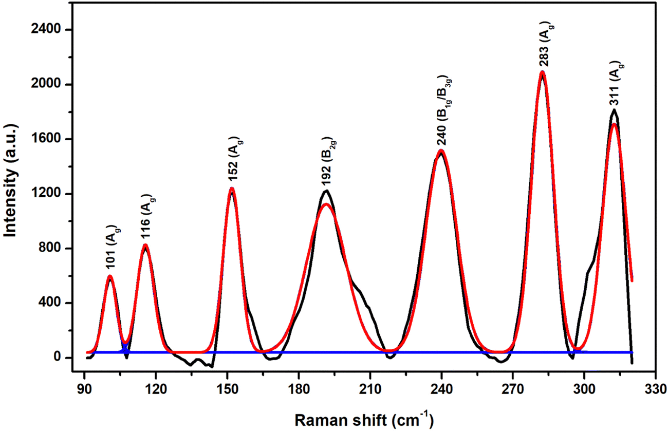
Fig. 3 demonstrates the Raman spectrum of as-deposited Sb2S3 on FTO. The clearly defined peaks show that the material is crystalline. It was found that the Sb2S3 stibnite phase exhibited well-resolved Raman bands at 101, 116, 152, 192, 240, 283, and 311 cm−1. The obtained peak positions correspond to the theoretically predicted Ag (at 101, 116, 152, 283, and 311 cm−1), B2g (at 192 cm−1), and B1g/B3g (at 240 cm−1) optical modes.51,52 The peaks are well-resolved, representing the crystalline nature of the sample. Well-determined Raman bands were observed at 159, 191, 240, 282, and 311 cm−1, conforming to the stibnite phase. The peaks at 283 and 311 cm−1 arise because of the symmetric vibration of the Sb2S3 pyramidal units having C3v symmetry53,54 and the peaks positioned at 192 and 240 cm−1 indicated the crystalline nature of Sb2S3.55,56
 | ||
| Fig. 3 Raman spectrum of the deposited Sb2S3 on FTO using Sb[(OC3H7)2S2P]3 as SSP. | ||
 | ||
| Fig. 4 (a) SEM micrograph (b) EDX elemental mapping (c) EDX spectrum with percentage of elements of the deposited Sb2S3 film on FTO. | ||
The elemental composition was ascertained by the EDX measurements. The EDX spectrum of the synthesized Sb2S3 material confirmed the pure nature of the sample. Fig. 4c illustrates the Sb2S3 matching EDX spectra. The samples included O, Sb, and S, as determined from the elemental composition of Sb2S3. Long exposure to air during analysis57 or the FTO substrate may have caused the oxygen atom to exist. Moreover, according to an EDX examination, the stoichiometric ratio of Sb:S was calculated to be 2.1:3. Furthermore, the presence of phosphorus impurities decreased with an increase in the reaction time as displayed in Fig. S8b and S9b (ESI†). Fig. 4b depicts an appropriate elemental mapping of Sb and S using energy-dispersive X-ray spectroscopy (EDS), demonstrating that Sb and S were uniformly distributed across the whole Sb2S3. Therefore, the reaction time of 24 h is considered as the optimized time and further characterization and resistive switching were performed. Cross-sectional SEM revealed that the majority of the particles are consistently aligned with their flat sides perpendicular to the substrate surface and that the film has a thickness of between 10–20 μm (Fig. S11, ESI†).
Fig. 5 depicts the TEM, SAED and HRTEM micrographs of the Sb2S3 powder which were obtained after scraping from the deposited Sb2S3 film via the in situ solvothermal process. To learn more about the shape and structure of the Sb2S3 additional investigation was performed using TEM, SAED, and HRTEM. Fig. S10 (ESI†) presents the size distribution histogram of Sb2S3, which showed a mean size of the rods of 523nm. Fig. 5a displays single crystal Sb2S3 with a width of 467 nm. Fig. 5b and c indicates a HRTEM image of single crystal Sb2S3. Fig. 5b depicts the SAED pattern which indicates the single crystal Sb2S3. The SAED pattern of the Sb2S3 unveils a spot design from the (120), (220), (200), and (240) planes, indicating that the Sb2S3 have an orthorhombic phase of Sb2S3 (ICDD:42-1393), and it resulted in a single crystal. The HRTEM image (Fig. 5c) indicates the lattice spacing of 0.36 nm corresponding to the (1 3 0) plane of orthorhombic phase of Sb2S3 (ICDD: 42-1393). This is perpendicular to the (0 1 0) plane which indicates the direction for the growth of Sb2S3 rods.58,59
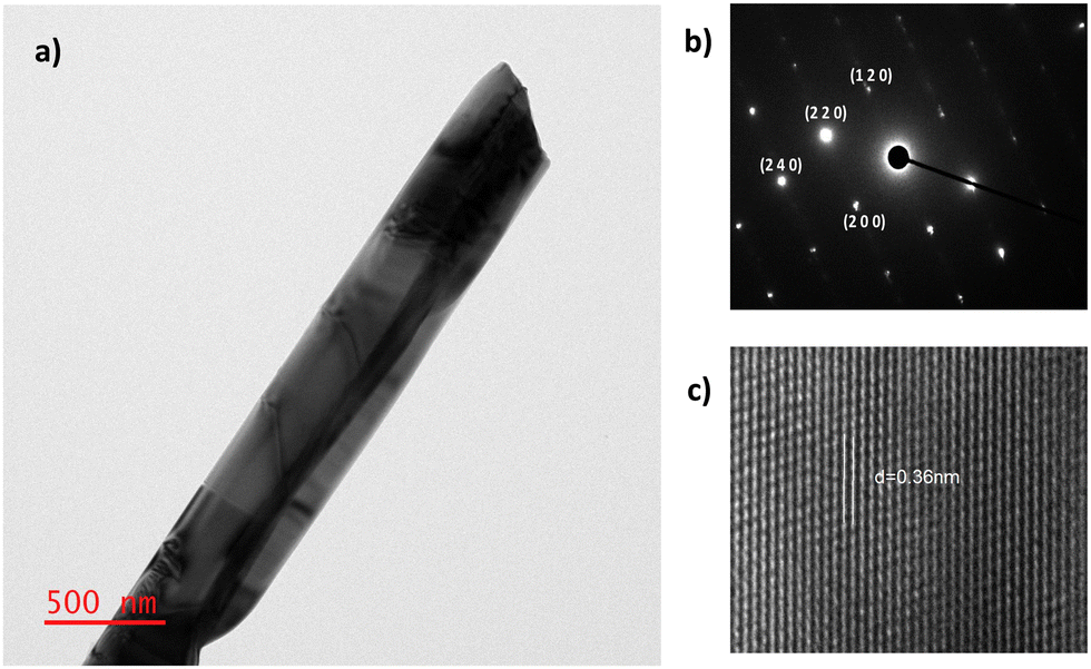 | ||
| Fig. 5 (a) TEM micrograph (b) SAED pattern, and (c) phase contrast HRTEM micrograph of Sb2S3. | ||
| (αhν) = A(hν − Eg)n | (2) |
 | ||
| Fig. 6 (a) UV-Vis spectrum and the (b) corresponding Tauc plot of the deposited Sb2S3 on FTO. | ||
3.4 Sb2S3 films for resistive random-access memory applications
The memristive switching properties of the as-deposited Sb2S3 film were investigated for application in RRAM devices. Fig. 7a illustrates the structure of our memory where the Sb2S3 film is sandwiched between the thermally evaporated silver top electrodes and the FTO bottom electrodes. The memristor was then subjected to a series of DC sweeps between the two electrodes for switching. As shown in Fig. 7b, the pristine device presents a high-resistance state (HRS) and can be switched to a low-resistance state (LRS) by applying a negative DC sweep where a SET voltage of approximately −1.3 V was observed. The device can then be reset back to the HRS by applying a successive positive sweep voltage (from 0 V to 2 V). Interestingly, the subsequent switching cycle highly resembles the first one with similar SET and RESET voltages. This suggests that no extra energy is required to initialize our device and it possesses electroforming-free properties. Consecutive cyclic I–V measurements were performed on the device to investigate the switching repeatability. Fig. 7c presents 80 cyclic I–V curves where the memristor maintains an ON/OFF ratio of ca. 10 (shown in Fig. 7d). The retention of the memristor is plotted in Fig. 7e where both HRS and LRS remain stable for over 1000 s, confirming its non-volatile switching behaviour. We further investigated the device-to-device variation of our memristor. Fig. 7f plots the representative DC switching characteristic of three different Sb2S3 memristors in this work. It can be observed that all three devices demonstrate very similar bipolar switching behaviour with negative SET and positive RESET voltages. There are some variations in the switching currents which are likely due to the non-uniformity of the Sb2S3 film deposited via our novel precursor and deposition approach. This can be improved with further optimisation of the deposition process. | ||
| Fig. 7 Resistive switching properties of the deposited Sb2S3 RRAM devices. (a) Schematic structure of Sb2S3-based memory devices. (b) The DC I–V curves of the electro-forming and subsequent switching cycles. (c) 80 consecutive DC I–V cycles of the device. (d) DC endurance, and (e) retention of the memristor. (f) Representative DC I–V cycles from three different devices. (g) I–V curve fitting using a SCLC model. (h) I–V switching characteristics of the memristor with a top electrode side length of 250 μm and 150 μm. (i) Both HRS and LRS of the memristor as a function of device area. | ||
The conduction mechanism of our memristor is investigated by fitting the I–V curve on a log scale as shown in Fig. 7g. According to the fitting, the conduction at the HRS is dominated by the Space-Charge-Limited-Current (SCLC).1 The device exhibits a linear relationship of current with applied voltage initially between 0 V and 0.4 V. This may be attributed to an Ohmic conduction mechanism resulting from thermally produced charge carriers.61 The slope increases to around 2 at higher applied voltages (0.4 ≤ V ≤ 1.1 V), and the current reveals the voltage square dependency, which is caused by the trap-controlled space charge limited current (TC-SCLC). Ohmic conduction dominates the conduction mechanism in the LRS, with the current linearly varying with the applied voltage.
To further elucidate the switching mechanism of our Sb2S3 memristor, we conducted an area dependence investigation. Fig. 7h presents the I–V characteristics for devices with areas of 150 μm by 150 μm and 250 μm by 250 μm. Despite showing similar I–V curves, some discrepancies can be observed between the two devices at the OFF state. We further plot the obtained HRS and LRS as a function of device area in Fig. 7i. It is evident that the HRS decreases with the increasing device area while the LRS is independent of the area. Such area-independence in the LRS suggests the filamentary switching mechanism of our Sb2S3 based memristor. However, the formation of the conductive filament is unlikely due to the top Ag electrode as it will require a positive bias to switch the device ON, which is in contrary to our observation. Instead, atoms originated in the as-deposited Sb2S3 film are likely to be responsible for the resistive switching. As a cation-like species in alloys, Sb can ionize and move upon application of a sufficient electric field.21 Application of a negative potential to the top electrode attracts the cationic Sb species to the top electrode, where neutral Sb atoms are accumulated and start to form a filament. This is reasonable for our memristor as our Sb2S3 film is slightly Sb-rich (Sb:S ratio 2.1:3). The readily available Sb atoms in the film also facilitate the initial switching process without the requirement of a larger electroforming voltage. Similar switching behaviour was also observed in other Sb2S3 based memory devices.34 We further confirmed this mechanism by replacing Ag with W (an inert metal) as the top electrode. Similar I–V characteristics were observed as shown in Fig. S12 (ESI†). The pristine memristor can be switched to a low resistance state under a similar negative bias and back to a high resistance state with a positive bias. This similar switching behaviour with an inert electrode further supports our argument that Sb-filament based switching is the dominant mechanism for our memristor.
Fig. 8 illustrates the schematics of the potential switching mechanism of our Sb2S3 based memory device. As-deposited Sb2S3 has a significant number of Sb atoms (Fig. 8a). Upon application of a strong enough electric field, these cation-like entities can ionise and move.21 When a negative potential is applied, the cationic Sb species are drawn to the top electrode, where neutral Sb atoms are gathered to form the filament. When the growing filament reaches the bottom electrode, the device changes to the LRS (SET process, as illustrated in Fig. 8b). A reverse bias, on the other hand, will cause the device to return to the HRS by displacing the cationic Sb species to the bottom electrode and dissolving the prepared filament (the RESET process, as depicted in Fig. 8c).
 | ||
| Fig. 8 Schematic of the filamentary-based resistive switching mechanism of our Ag/Sb2S3/FTO resistive memory cell. | ||
We further compared the resistive switching performance of our Ag/Sb2S3/FTO memristor with other reported metal sulfide-based RRAM devices in Table 1. Our device has competitive performance with unique electroforming-free properties. More importantly, the successful demonstration of memristive behaviour has certainly paved the way for future large-scale manufacturing of functional chalcogenide thin films using our novel one-step, facile, low-temperature in situ solvothermal deposition approach.
| S. no. | Device structure | Electroforming required | Retention (s) | On/off ratio | V set (V) | V reset (V) | Ref. |
|---|---|---|---|---|---|---|---|
| 1 | Ag/Sb 2 S 3 /FTO | No | 10 4 | 10 | −1.3 | 2 | This work |
| 2 | Cu/ZnS/Pt | Yes | — | 10–108 | ∼0.6 | ∼−0.7 | 62 |
| 3 | Cu/ZnS/ITO | Yes | — | 10–108 | ∼0.6 | ∼−1.2 | 62 |
| 4 | Cu/MoS2/Ni–Mn–In on Si | Yes | 103 | 6 × 10² | 1.36 | 0.98 | 63 |
| 5 | Graphene/MoS2−xOx/graphene | Yes | ∼105 | 102 | 3.5 | −4.8 | 64 |
4. Conclusions
In this study, we reported the in situ solvothermal process which serves as an alternative low temperature solution-based deposition of Sb2S3 films from [Sb{S2P{O(Pr)2}3] as a SSP to demonstrate scalable and industrially compatible processing for memristive devices. The proposed solution processible route is advantageous as it demonstrates ease of stoichiometric modulation, low equipment and energy cost and high throughput production. Here, the process was performed without involvement of any binding agent and hence the additional step of annealing is eliminated. The deposited film was pure, uniform, and well-adhered, revealing the crystalline orthorhombic stibnite phase. Significantly, the deposited Sb2S3 film was employed as a novel resistive random-access memory device and it demonstrated typical bipolar resistive switching behaviour with electroforming-free properties. The Ag/Sb2S3/FTO memristive device showed reliable stability over 80 cycles while maintaining an ON/OFF ratio of ca. 10. The switching behaviour is attributed to the formation and rupture of Sb ion-based filaments within the Sb2S3 matrix. This further opens up wide range of possibilities for futurelow power and high performance devices.Author contributions
Sayali Shrishail Harke: conceptualization, methodology, investigation, validation, formal analysis, and writing – original draft. Tongjun Zhang: methodology and writing – review & editing. Ruomeng Huang: methodology, and writing – review & editing. Chitra Gurnani: conceptualization, methodology, validation, formal analysis, writing – review & editing, and supervision.Conflicts of interest
There are no conflicts to declare.Acknowledgements
The authors are grateful to Mahindra University, Hyderabad, for providing the necessary funds and experimental resources to conduct the work. The authors thank SAIF Chandigarh Punjab University for access to NMR characterization facility. We also acknowledge the School of Physics and School of Chemistry, University of Hyderabad, for TEM and SEM characterisation, respectively.References
- A. H. Jaafar, L. Meng, Y. J. Noori, W. Zhang, Y. Han, R. Beanland, D. C. Smith, G. Reid, K. De Groot, R. Huang and P. N. Bartlett, J. Phys. Chem. C, 2021, 125, 26247–26255 CrossRef CAS.
- R. Huang, K. Sun, K. S. Kiang, K. A. Morgan and C. H. De Groot, Microelectron. Eng., 2016, 161, 7–12 CrossRef CAS.
- A. H. Jaafar, M. O’Neill, S. M. Kelly, E. Verrelli and N. T. Kemp, Adv. Electron. Mater., 2019, 5, 1900197 CrossRef.
- M. J. Lee, C. B. Lee, D. Lee, S. R. Lee, M. Chang, J. H. Hur, Y. B. Kim, C. J. Kim, D. H. Seo, S. Seo, U. I. Chung, I. K. Yoo and K. Kim, Nat. Mater., 2011, 10, 625–630 CrossRef CAS PubMed.
- D. I. Son, D. H. Park, J. Bin Kim, J.-W. Choi, T. W. Kim, B. Angadi, Y. Yi and W. K. Choi, J. Phys. Chem. C, 2011, 115, 2341–2348 CrossRef CAS.
- G. U. Kamble, A. P. Patil, R. K. Kamat, J. H. Kim and T. D. Dongale, ACS Appl. Electron. Mater., 2023, 5, 2454–2481 CrossRef CAS.
- V. K. Nagareddy, M. D. Barnes, F. Zipoli, K. T. Lai, A. M. Alexeev, M. F. Craciun and C. David Wright, ACS Nano, 2017, 11, 3010–3021 CrossRef CAS PubMed.
- P. Priyadarshini, S. Das and R. Naik, RSC Adv., 2022, 12, 9599–9620 RSC.
- V. Gupta, S. Kapur, S. Saurabh and A. Grover, IETE Tech. Rev., 2020, 37, 377–390 CrossRef.
- K. C. Kwon, J. H. Baek, K. Hong, S. Y. Kim and H. W. Jang, Nano-Micro Lett., 2022, 14, 1–30 CrossRef PubMed.
- W. Banerjee, Electronics, 2020, 9, 1–24 CrossRef.
- Z. Jiang, Y. Wu, S. Yu, L. Yang, K. Song, Z. Karim and H. S. P. Wong, IEEE Trans. Electron Devices, 2016, 63, 1884–1892 CAS.
- K. H. Nam, J. H. Kim, W. J. Cho, C. H. Kim and H. B. Chung, J. Nanosci. Nanotechnol., 2016, 16, 10393–10396 CrossRef CAS.
- J. H. Lee, S. P. Park, K. Park and H. J. Kim, Adv. Funct. Mater., 2020, 30, 1907437 CrossRef CAS.
- E. J. Yoo, M. Lyu, J. H. Yun, C. J. Kang, Y. J. Choi and L. Wang, Adv. Mater., 2015, 27, 6170–6175 CrossRef CAS PubMed.
- A. P. Rananavare, S. J. Kadam, S. V. Prabhu, S. S. Chavan, P. V. Anbhule and T. D. Dongale, Mater. Lett., 2018, 232, 99–102 CrossRef CAS.
- C. Schindler, M. Meier, R. Waser and M. N. Kozicki, Proc. – 2007 Non-Volatile Mem. Technol. Symp. NVMTS 07, 2007, pp. 82–85.
- N. I. Mou and M. Tabib-Azar, Appl. Surf. Sci., 2015, 340, 138–142 CrossRef CAS.
- H. Hönigschmid, M. Angerbauer, S. Dietrich, M. Dimitrova, D. Gogl, C. Liaw, M. Markert, R. Symanczyk, L. Altimime, S. Bournat and G. Müller, IEEE Symp. VLSI Circuits, Dig. Tech. Pap., 2006, vol. 42, pp. 110–111.
- N. Banno, T. Sakamoto, T. Hasegawa, K. Terabe and M. Aono, Jpn. J. Appl. Phys., Part 1, 2006, 45, 3666–3668 CrossRef CAS.
- S. Yoo, T. Eom, T. Gwon and C. S. Hwang, Nanoscale, 2015, 7, 6340–6347 RSC.
- T. D. Dongale, N. D. Desai, K. V. Khot, N. B. Mullani, P. S. Pawar, R. S. Tikke, V. B. Patil, P. P. Waifalkar, P. B. Patil, R. K. Kamat, P. S. Patil and P. N. Bhosale, J. Solid State Electrochem., 2017, 21, 2753–2757 CrossRef CAS.
- P. S. Pawar, R. S. Tikke, V. B. Patil, N. B. Mullani, P. P. Waifalkar, K. V. Khot, A. M. Teli, A. D. Sheikh and T. D. Dongale, Mater. Sci. Semicond. Process., 2017, 71, 102–108 CrossRef CAS.
- L. Zhang, C. Wu, W. Liu, S. Yang, M. Wang, T. Chen and C. Zhu, J. Mater. Chem. A, 2018, 6, 21320–21326 RSC.
- R. Boughalmi, A. Boukhachem, M. Kahlaoui, H. Maghraoui and M. Amlouk, Mater. Sci. Semicond. Process., 2014, 26, 593–602 CrossRef CAS.
- P. Makreski, G. Petruševski, S. Ugarković and G. Jovanovski, Vib. Spectrosc., 2013, 68, 177–182 CrossRef CAS.
- K. F. Abd-El-Rahman and A. A. A. Darwish, Curr. Appl. Phys., 2011, 11, 1265–1268 CrossRef.
- F. Aousgi and M. Kanzari, Energy Procedia, 2011, 10, 313–322 CrossRef CAS.
- X. Wang, R. Tang, C. Wu, C. Zhu and T. Chen, J. Energy Chem., 2018, 27, 713–721 CrossRef.
- P. Zhong, J. Xie, R. Bagheri, Q. Yi, Q. Chen, J. Tan, L. He, F. Zhang, L. Zhang and G. Zou, Chem. Commun., 2019, 55, 14530–14533 RSC.
- O. Savadogo and K. C. Mandal, Sol. Energy Mater. Sol. Cells, 1992, 26, 117–136 CrossRef CAS.
- W. Yi, F. Perner, M. S. Qureshi, H. Abdalla, M. D. Pickett, J. J. Yang, M. X. M. Zhang, G. Medeiros-Ribeiro and R. S. Williams, Appl. Phys. A: Mater. Sci. Process., 2011, 102, 973–982 CrossRef CAS.
- W. Wu, B. Shan, K. Feng and H. Nan, Mater. Sci. Semicond. Process., 2016, 44, 18–22 CrossRef CAS.
- A. G. Wallace, R. P. King, N. Zhelev, A. H. Jaafar, W. Levason, R. Huang, G. Reid and P. N. Bartlett, Electrochim. Acta, 2022, 432, 141162 CrossRef CAS.
- C. Gurnani, S. L. Hawken, A. L. Hector, R. Huang, M. Jura, W. Levason, J. Perkins, G. Reid and G. B. G. Stenning, Dalton Trans., 2018, 47, 2628–2637 RSC.
- M. A. Malik, N. Revaprasadu and P. O’Brien, Chem. Mater., 2001, 13, 913–920 CrossRef CAS.
- J. Rodriguez-Castro, P. Dale, M. F. Mahon, K. C. Molloy and L. M. Peter, Chem. Mater., 2007, 19, 3219–3226 CrossRef CAS.
- G. Murtaza, M. Akhtar, M. Azad Malik, P. O’Brien and N. Revaprasadu, Mater. Sci. Semicond. Process., 2015, 40, 643–649 CrossRef CAS.
- D. C. Onwudiwe, O. C. Olatunde and S. Mathur, Phys. B, 2021, 605, 412691 CrossRef CAS.
- W. Lou, M. Chen, X. Wang and W. Liu, Chem. Mater., 2007, 19, 872–878 CrossRef CAS.
- J. R. Castro, K. C. Molloy, Y. Liu, C. S. Lai, Z. Dong, T. J. White and E. R. T. Tiekink, J. Mater. Chem., 2008, 18, 5399–5405 RSC.
- A. L. Bingham, J. E. Drake, C. Gurnani, M. B. Hursthouse, M. E. Light, M. Nirwan and R. Ratnani, J. Chem. Crystallogr., 2006, 36, 627–630 CrossRef CAS.
- J. L. Lefferts, K. C. Molloy, J. J. Zuckerman, I. Haiduc, C. Guta and D. Ruse, Inorg. Chem., 1980, 19, 1662–1670 CrossRef CAS.
- I. Haiduc, D. B. Sowerby and S. F. Lu, Polyhedron, 1995, 14, 3389–3472 CrossRef CAS.
- M. Wieber and M. Schröpf, Phosphorus, Sulfur Silicon Relat. Elem., 1995, 102, 265–277 CrossRef CAS.
- J. S. Yadav, R. K. Mehrotra and G. Srivastava, Polyhedron, 1987, 6, 1687–1693 CrossRef CAS.
- C. Glidewell, Inorg. Chim. Acta, 1977, 25, 159–163 CrossRef CAS.
- Y. J. Zhu and F. Chen, Chem. Rev., 2014, 114, 6462–6555 CrossRef CAS PubMed.
- P. G. Sheikhiabadi, M. Salavati-Niasari and F. Davar, Mater. Lett., 2012, 71, 168–171 CrossRef CAS.
- W. D. Xiang, G. Y. Ji, W. Jing, Y. X. Yang and X. N. Liu, Glass Phys. Chem., 2012, 38, 245–253 CrossRef CAS.
- M. Delaney, I. Zeimpekis, D. Lawson, D. W. Hewak and O. L. Muskens, Adv. Funct. Mater., 2020, 30, 1–10 CrossRef.
- R. Parize, A. Katerski, I. Gromyko, L. Rapenne, H. Roussel, E. Kärber, E. Appert, M. Krunks and V. Consonni, J. Phys. Chem. C, 2017, 121, 9672–9680 CrossRef CAS.
- R. G. Sotelo Marquina, T. G. Sanchez, N. R. Mathews and X. Mathew, Mater. Res. Bull., 2017, 90, 285–294 CrossRef CAS.
- J. S. Eensalu, K. Tõnsuaadu, I. Oja Acik and M. Krunks, Mater. Sci. Semicond. Process., 2022, 137, 106209 CrossRef CAS.
- B. B. H. Juμrez, S. Rubio, J. Sμnchez-dehesa and C. Lopez, Adv. Mater., 2002, 14, 1486–1490 CrossRef.
- S. M. Hwang, J. Kim, Y. Kim and Y. Kim, J. Mater. Chem. A, 2016, 4, 17946–17951 RSC.
- S. Mourdikoudis and L. M. Liz-Marza, Chem. Mater., 2013, 25, 1465–1476 CrossRef CAS.
- R. Almalki, E. M. Mkawi and Y. Al-Hadeethi, J. Mater. Sci.: Mater. Electron., 2020, 31, 9203–9211 CrossRef CAS.
- G. Shen, D. Chen, K. Tang, X. Jiang and Y. Qian, J. Cryst. Growth, 2003, 252, 350–354 CrossRef CAS.
- M. Lajnef and H. Ezzaouia, Open Appl. Phys. J., 2009, 2, 23–26 CrossRef CAS.
- R. Huang, X. Yan, K. A. Morgan, M. D. B. Charlton and C. H. De Groot, J. Phys. D: Appl. Phys., 2017, 50, 175101 CrossRef.
- F. Zhuge, K. Li, B. Fu, H. Zhang, J. Li, H. Chen, L. Liang, J. Gao, H. Cao, Z. Liu and H. Luo, AIP Adv., 2015, 5, 1–8 Search PubMed.
- A. Kumar, S. Pawar, S. Sharma and D. Kaur, Appl. Phys. Lett., 2018, 112, 1–5 Search PubMed.
- M. Wang, S. Cai, C. Pan, C. Wang, X. Lian, Y. Zhuo, K. Xu, T. Cao, X. Pan, B. Wang, S. J. Liang, J. J. Yang, P. Wang and F. Miao, Nat. Electron., 2018, 1, 130–136 CrossRef CAS.
Footnote |
| † Electronic supplementary information (ESI) available: Original IR, 1H, and 31P{1H} NMR spectroscopic data for [Et3NH][(OC3H7)2S2P] and [Sb{S2P{O(Pr)2}3], the size distribution histogram and cross-sectional view of deposited Sb2S3 on the FTO substrate and bipolar non-volatile resistive switching behaviours plot of the W/Sb2S3/FTO. See DOI: https://doi.org/10.1039/d3ma00205e |
| This journal is © The Royal Society of Chemistry 2023 |