
 Open Access Article
 This Open Access Article is licensed under a
 Creative Commons Attribution 3.0 Unported Licence
Elucidating the role of disorder introduced by nitrogen in the superconducting properties of tungsten thin films
J. A.
Hofer
 *a,
S.
Bengio
b,
S.
Suárez
ac and
N.
Haberkorn
ab
*a,
S.
Bengio
b,
S.
Suárez
ac and
N.
Haberkorn
ab
aInstituto Balseiro, Universidad Nacional de Cuyo and Comisión Nacional de Energía Atómica, Av. Bustillo 9500, 8400 San Carlos de Bariloche, Argentina. E-mail: juan.hofer@cab.cnea.gov.ar; Tel: +54 9 294 444 5171
bComisión Nacional de Energía Atómica and Consejo Nacional de Investigaciones Científicas y Técnicas, Centro Atómico Bariloche, Av. Bustillo 9500, 8400 San Carlos de Bariloche, Argentina
cComisión Nacional de Energía Atómica., Centro Atómico Bariloche, Av. Bustillo 9500, 8400 San Carlos de Bariloche, Argentina
First published on 8th November 2022
Abstract
Tungsten thin films are successfully prepared by reactive sputtering at room temperature using different Ar/N2 gas mixtures. The role of disorder and chemical composition in the presence of superconductivity is analyzed. The results show that the crystalline structure of the samples changes drastically due to nitrogen in the mixture increases. A small addition of nitrogen stabilizes the metastable β-W phase, which successively increases its disorder as more nitrogen is added. These changes in the microstructure manifest as an increment in the lattice parameter followed by an amorphization. The electrical transport shows that the β-W stabilized at low N2 concentrations does not display superconductivity above 2.5 K. Superconductivity with Tc between 4 K and 4.7 K emerges for disordered β-W and remains in amorphous films. A detailed study of the chemical state and composition indicates that superconductivity may be related more to amorphous structures (nitrides + W) and strained β-W than to β-W as it is stabilized with low nitrogen impurities.
Introduction
Tungsten is characterized by two different phases: alpha (α)-W (body-centered cubic structure) and beta (β)-W (A15 structure).1 The latter is metastable,2 and it is usually stabilized in sputtered films by modifying the deposition parameters3 or adding nitrogen4,5 or oxygen impurities in a reactive atmosphere.6–9 The electrical resistivity of β-W is much higher than that of α-W.1 Moreover, it displays high spin–orbit coupling (SOC) and type II superconductivity has been observed in disordered thin films.3,5,10 The SOC converts the material into an exciting candidate for applications in spintronics.5,6,11 On the other hand, superconductivity with a critical temperature (Tc) ranging from 3 to 5 K may be relevant for fabricating devices such as superconducting nanowire single-photon detectors (SNSPDs).12 However, the origin of superconductivity in disordered W films is unclear. When nitrogen impurities stabilize the β-phase, the films display Tc up to 4.7 K.5 The figure agrees with reports for amorphous structures obtained by focused ion beam (FIB) assisted deposition,13–16 suggesting that disorder at the nanoscale plays a role in the superconducting properties of W nanostructures. Indeed, nanowires with Tc ≈ 4.8 K were obtained by FIB using tungsten hexacarbonyl and a gallium beam where the impurities were mainly C, Ga and O.13–15 Consequently, one would expect that the origin of superconductivity reported in β-W may be strongly affected by the coexistence of amorphous structures induced by the presence of impurities and disorder.5,17,18 Regarding nitrides WNx (W/N ≥ 1), the system displays two main stable phases: low-temperature hexagonal h-WN and high-temperature cubic c-WN and tungsten subnitride W2N.19 Superconductivity has only been reported for disordered (β-W + WNx) thin film growth by reactive sputtering.17Here, we performed a detailed study of the effect of nitrogen addition on the superconducting properties of W thin films grown by reactive sputtering on silicon substrates. We modified the N2/Ar ratio in the reactive atmosphere within a range where the film's structure evolved from nanocrystalline (α + β-W) to W amorphous (with high nitrogen content). The crystalline structure was studied by X-ray diffraction (XRD), and its chemical composition was determined using high-resolution X-ray photoelectron spectroscopy (XPS). The structural information was compared with electrical transport measurements to elucidate the origin of the superconducting behavior in nanocrystalline and amorphous W-based thin films.
Results and discussion
Fig. 1a shows a typical AFM image for a 19.5 nm thick W15 film. The surface is highly flat and free of defects,20 as evidenced in the surface roughness profile shown in Fig. 1b. Similar morphologies are usually observed for the films independent of the nitrogen concentration used in the reactive mixture. Fig. 1c shows a low-angle X-ray diffraction pattern and the fit using Parrat32 code.21 The data is characterized by well-defined maxima and minima, indicating low roughness and agreeing with the quantification obtained by the AFM images. The growth rate reduces as nitrogen increases in the gas mixture, being 21 nm min−1 for a little amount of nitrogen and reducing to ≈18 nm min−1 for 30% nitrogen (Table 1).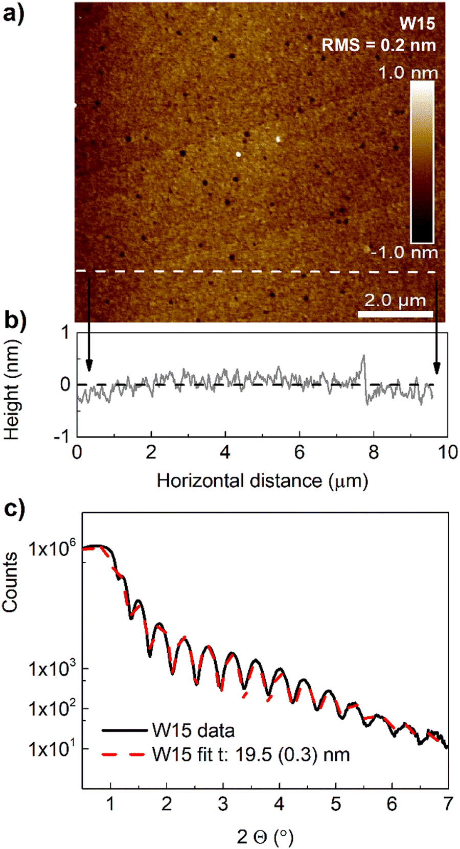 | ||
| Fig. 1 (a) AFM image for a typical W film. (b) Surface roughness profile. (c) Low angle X-ray data and the fitting for a W15 thin film. | ||
| N2 (%) | a (nm) | Growth rate (nm min−1) | T c (K) | RRR | ρ 10K (μΩ m) | H C2(0) (T) |
|---|---|---|---|---|---|---|
| 0 | 0.505 | — | 0.2 | |||
| 1 | 0.510 | 20.5 | — | 1.02 | 1.5 | — |
| 3 | 0.512 | 20.1 | — | 1.00 | 1.75 | — |
| 5 | 0.526 | 19.6 | 3.33 | 0.99 | 1.9 | 3.50 |
| 7 | 0.530 | 19.5 | 4.24 | 0.97 | 1.8 | 5.35 |
| 8 | 0.531 | 19.5 | 4.46 | 0.98 | 1.9 | — |
| 10 | 0.531 | 19.5 | 4.53 | 0.98 | 2.2 | 5.60 |
| 15 | — | 18.2 | 4.72 | 0.99 | 2.6 | 5.90 |
| 20 | — | 18.1 | 4.67 | 0.98 | 3.1 | 5.90 |
| 25 | — | 18.3 | 4.43 | 0.97 | 3.1 | — |
| 30 | — | 17.8 | 4.70 | 0.97 | — | 5.90 |
Fig. 2 shows XRD data for several films grown in different reactive atmospheres for 3 minutes. The results show appreciable changes as the nitrogen in the reactive atmosphere increases. The film growth in pure argon displays a unique asymmetric peak centered at 2θ ≈ 39.8°. The asymmetry to higher angles suggests that it corresponds to an overlapping of the reflections (210)β and (110)α.1–3 For nitrogen concentrations between 0.5 and 10%, the patterns display the reflections (200)β, (210)β and (211)β. Between 1 and ≈7%, the position of the peaks reduces in angle. Indeed, (210)β systematically shifts from 39.44° to 39.18°, indicating that interstitial N2 increases the lattice parameter. In contrast, at concentrations between 7 and 10%, the peak intensity systematically reduces to disappear at ≈12%. No appreciable changes, with a broad and low-intensity peak at 2θ ≈ 39°, are observed for concentrations between 12% and 30%. Table 1 shows a summary of the lattice parameter for β-phase. Applying the Scherrer equation at the (210)β peak, we estimate a grain size smaller than the film thickness, being ≈20 nm for low nitrogen concentrations and ≈10 nm before the collapse in an amorphous structure (≈10%).
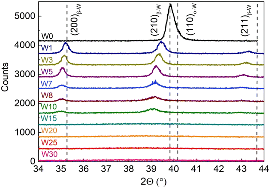 | ||
| Fig. 2 X-ray data for W film growth using different reactive Ar/N2 atmospheres. The thickness for all the films is ≈60 nm. | ||
Fig. 3a shows the temperature dependence of normalized resistance (R/R10K) for 20 nm thick W films. The thickness was selected considering the lower limit where bulk behavior is expected.
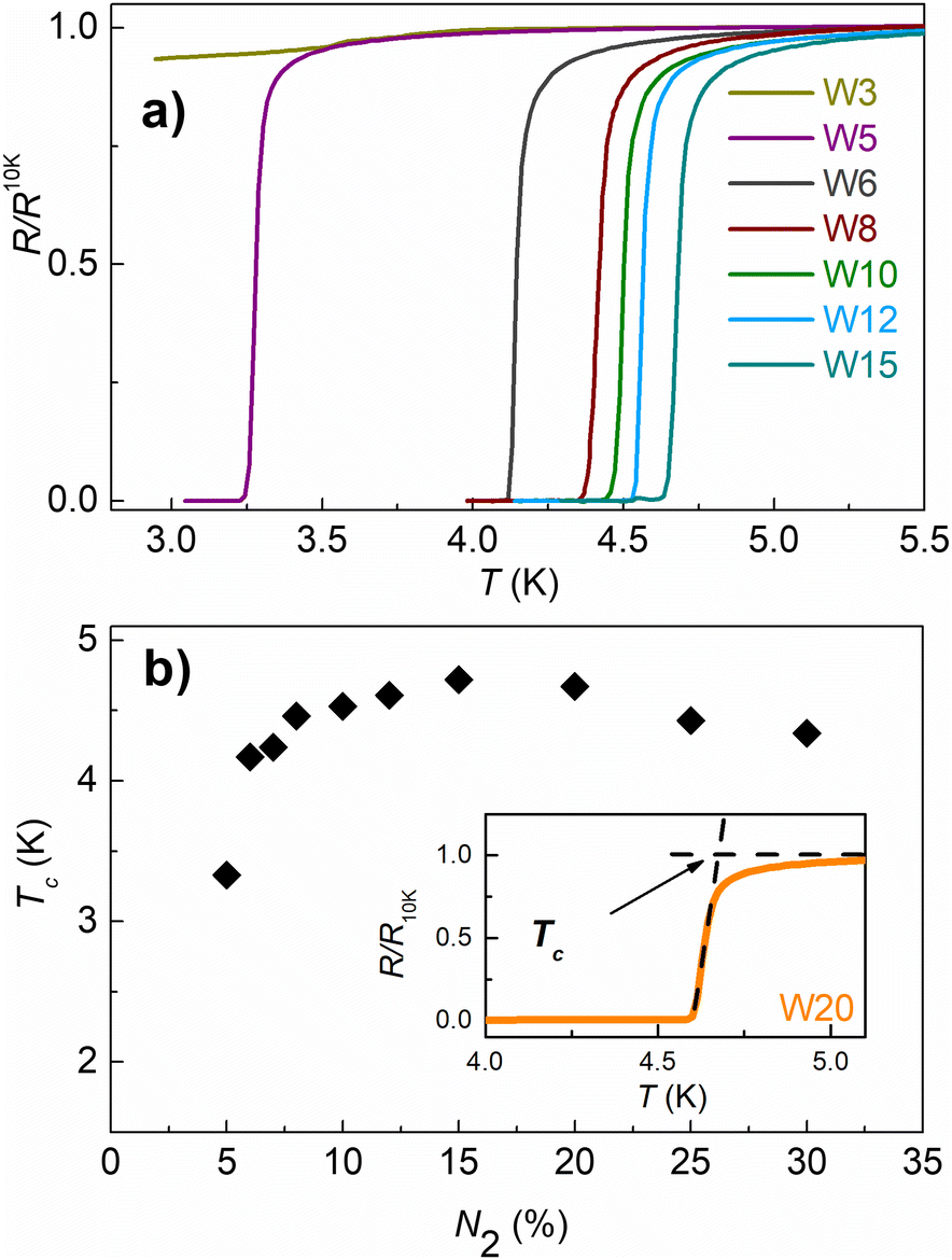 | ||
| Fig. 3 (a) Temperature dependence of the normalized resistivity for films grown for 1 minute using different reactive Ar/N2 atmospheres (thickness between 18 and 20 nm). (b) Summary of the superconducting critical temperature as a function of the N2 concentration in the reactive gas mixture. | ||
Moreover, superconducting devices usually require films with thicknesses of a few nanometers. W0 and W1 were not included because they do not show any feature of superconductivity in the measured range of temperature. The residual resistivity ratio (RRR) is close to one in all the films grown using a reactive atmosphere. This value corresponds to disordered structures with a very short electron mean free path (l). The resistivity values at 10 K increase faster, adding a small amount of nitrogen from 0.2 to 1.5 to 2 μΩ m for β-phase films and increasing to 3 μΩ m for amorphous samples rich in nitrogen (see Table 1). The results show that superconductivity with percolation and Tc = 3.3 K appears for W5. As nitrogen in the gas mixture increases to 30%, Tc remains between 4 and 4.7 K reaching a maximum for W15 (see Fig. 3b). This dependence implies that the superconducting behavior does not come from the initially stabilized β-W but rather from the addition of disorder produced by interstitial nitrogen (evidenced in the lattice parameter) or coexistence with amorphous structures. The latter may be a consequence of disordered W or nitrides.15,17
To compare the samples beyond Tc, we measured the upper critical fields (Hc2) as a function of temperature for the different films. Magnetic field (H) was applied perpendicular to the surface (S). Fig. 4 summarizes the results using T/Tc at the x-axis. The inset corresponds to the curves using the absolute temperature. The dashed lines correspond to the fits using the Werthamer–Helfand–Hohenberg (WHH) model developed for dirty one-band superconductors.22 The data were fitted considering a Maki parameter α = 0 and spin–orbit scattering constant λso = 0. For α = 0, Hc2(T) is given as the pure “orbital field limit”, corresponding to supercurrents circulating around the vortex cores. The analysis is supported in which the films are highly disordered with a very short mean free path. Hc2(T) dependences are similar in all the films except for W5 with lower Tc. All μ0Hc2 (0) (<5.8 T) are lower than those expected from the Pauli limit Hp ≈ 1.84Tc (maximal possible magnetic field strength for a BCS superconductor). The coherence length estimated as  gives ξ(0) ≈ 7.5–7.8 nm for all the films with Tc higher than 4 K. The results also allow the estimation of the electron diffusion constant D=4kB/(πedHc2/dT) (where kB is the Boltzmann constant and e is the electron charge).23 The latter is a parameter essential to determine the recombination quasiparticle time (normal electron in Cooper pairs) from the flux-flow instability in micro- and nano-bridges of dirty superconductors.24D is around 0.45 cm2 s−1 for all films with Tc > 4 K. This value is similar to the reported for other dirty superconductors used in SNSPD.25
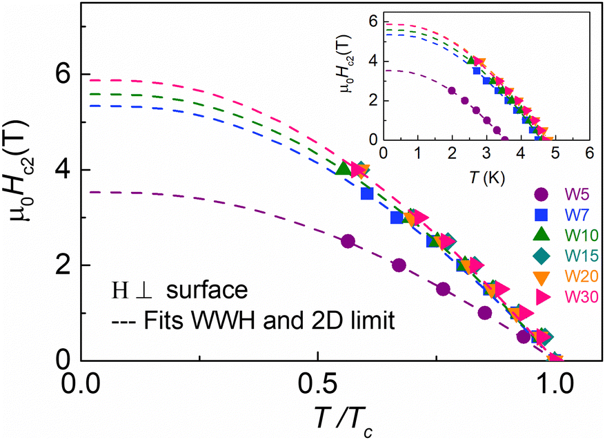 | ||
| Fig. 4 Upper critical field as a function of the reduced temperature (T/Tc) for 20 nm thick W thin film growth using different concentrations of N2 in the gas mixture. Inset: Similar to the main panel but with absolute temperature in the x-axis. Dashed lines correspond to the fit using the WHH model for dirty superconductors. | ||
Considering the similitude in the superconducting properties and the differences in the X-ray data, we performed XPS measurements to determine the chemical state of the W in the films. For completeness, a W thin film growth in a reactive gas mixture with 50% N2 was included.5 XPS measurements were performed to determine the surface chemical composition and chemical state of W films on a sequence of W-based surfaces prepared with increasing the N2 content in the Ar/N2 atmosphere during the synthesis, specifically with 0%, 1%, 5%, 10%, 15%, 25% and 50% of N2 content. The W4f and N1s spectra were analyzed for this sequence. Surface cleaning was performed with Ar+ sputtering (2 kV) for 15 min, after which the native oxide WO3 disappeared. Fig. 5 shows the W4f spectra as a function of increasing N2 content during the synthesis. The W4f spectrum consists of 4f7/2 and 4f5/2 spin–orbit doublet for each oxidation state. The spectra were fitted using Doniach-Sunjic profiles convoluted with Gaussian distributions plus a Shirley-type background. The total fitted intensities along with the experimental ones are shown in each spectrum. For W0, we observe a single component at BE ∼ 31.47 eV ascribed to the pure bulk W, in agreement with the reported values of BE ∼ 31.42eV for W (111) and W (001).26 For W1 and W5, we observe the appearance of a new component at lower BE, specifically at BE ∼ 31.22 eV, which can be assigned to the β-W phase reported at BE ∼ 31.08 eV,9 or amorphous W reported at BE ∼ 31.26 eV,9 or to a mixture of both. For W10, W15, and W25, a new prominent component shows up at BE ∼ 31.4 eV and a minor component at BE ∼ 32 eV. The latter can be related to WN0.2 and WN0.6, respectively.27,28 They appear simultaneously with an increment in the nitrogen content of the films, evidenced by the N1s peak, as discussed below.
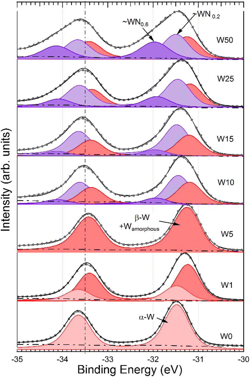 | ||
| Fig. 5 W4f spectra for W thin film growth in reactive gas mixtures with N2 (%): 0, 1, 5, 10, 15, 25, and 50. With the progressive enhancement of N2, we identified different W-based phases: α-W, β-W, amorphous W, WN0.2, and WN0.6. | ||
Fig. 6 displays the mentioned core-level spectra for W15, W25, and W50, with the same intensity axes at each stage. The N1s peak at BE ∼ 397.8 eV, compatible with nitrides,29 was identified in all cases. The nitrogen signals at W15 could be associated with the W4f component at BE ∼ 31.4 eV, from which we can estimate the relative concentration of W/N and associate it with the compound WN0.2 as obtained by I. Takano et al. using ion implantation.27 In W25 and W50, the N1s peak increases its intensity with the appearance of the W4f component at BE ∼ 32 eV, in agreement with the nitride phase reported by M. Wen et al.28 and D. Alegre et al.29 by plasma nitriding. From the relative concentration of W/N, we could associate it with the formation of ∼WN0.6.
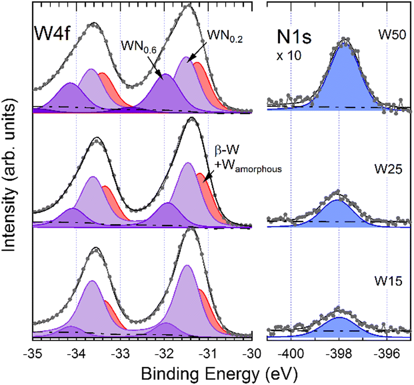 | ||
| Fig. 6 W4f and N1s spectra for W thin film growth in reactive gas mixtures with N2 (%): 15, 25, and 50. With the progressive incorporation of nitrogen, we identified different tungsten nitride phases: ∼WN0.2 and ∼WN0.6. | ||
The analysis of N1s and W4f peaks also allows a quantitative estimation of the N content. There is no direct relationship between N2 content in the atmosphere and the resultant stoichiometry. As mentioned above, nitrogen does not incorporate homogeneously in the films due to the coexistence of phases with different W/N ratios. The nitrogen in W5 is negligible but increases to WN0.2 for W15. On the other hand, the amount of nitrogen in W50 is close to twice the presence in W25. The latter is evidenced by a marked increase in the WN0.6 component (see Fig. 6).
The summary of results indicates a further correlation between superconductivity and disorder. The β-W stabilizes with a minor amount of nitrogen. However, superconductivity appears for reactive gas mixtures with 5% N2, where the lattice parameter of β-W increases due to interstitial disorder and possibly coexist with amorphous structures. For gas mixtures between 7% and 30%, Tc remains above 4 K, reaching a maximum of 4.7 K at 15%. These samples that initially display XRD peaks corresponding to β-W become amorphous as nitrogen increases in the gas mixture. The XPS data indicate the coexistence of β-W together with chemical bonding corresponding to nitrides. The different WNx are evident mainly as changes in the BE of the W component but have imperceptible changes in the BE of the N1s. A similar behavior was observed by Alegre et al. in thin films with different amounts of disorder.29 As we mentioned above, there is a slow diminution of Tc as the gas mixture increases above 15% and the amorphous phases are enriched in nitrogen. The latter indicates that, as in amorphous WSix and MoSix,30,31 the maximum Tc can be associated with specific stoichiometry and disorder. In our results, the temperature dependence and absolute values of the upper critical fields are similar in all the films, which shows that the nature of the superconductivity is the same.
A particular highlight of these samples is that they display Tc comparable to nanowires obtained by FIB.13–16 Moreover, the superconducting properties are similar to those observed in amorphous superconductors such as MoSi32 and WSi.33 The latter are materials typically used for designing SNSPD, characterized by fast response time. The devices require electrical and geometrical homogeneity to guarantee equal response through the wire.12 Considering that requirement, we test the magnetic field dependence of the critical current density of the samples performing IV curves at 3.5 K. The absolute values of Jc and its magnetic field dependence usually relate to a balance between intrinsic properties and vortex pinning produced by crystalline defects. Therefore, any severe change in the superconducting volume with chemical composition should be evident. For thin films with thickness lower than the penetration depth (λ), in addition to crystalline imperfections, the thickness fluctuations and edge quality impact Jc.23,34Fig. 7 shows Jc (H) for several representative samples. The measurements were performed with the magnetic field applied perpendicular to the surface. The inset to Fig. 7 shows typical IV curves in log–log scales and the criterion for Jc. The absolute values of Jc in all the samples are similar with a value of ≈2 × 10⁸ (A m−2) at μ0H = 0.012 T and these values drop fast as the magnetic field increases. Representing Jc (H) as a power-law with Jc ∝ B−α, α takes values ≈1.3. This magnitude in the α exponent is characteristic of films with negligible bulk vortex pinning, as expected for films with flat surfaces and defects smaller than 2ξ.35 The similitude in Jc(H) for samples suggests that inhomogeneities at the nanoscale produced by variations in the chemical environment of the W do not play a role in the vortex pinning. As mentioned above, Jc for all the films may be determined by edge barriers and possible variations of the strip profile.34 Indeed, increments of Jc up to 3 times have been reported for MoSi bridges via edge-quality improvement using milling by a focused ion beam.36
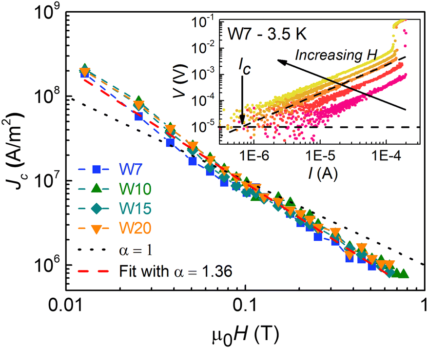 | ||
| Fig. 7 Magnetic field dependence of the critical current density, Jc, for films grown for 1 minute (thickness between 18 and 20 nm). The measurements were performed with the magnetic field perpendicular to the surface of the films. Inset: Typical IV curves in log-log scales and the criterion for the determination of Jc. | ||
Experiment
Nitrogen-doped W thin films were grown by reactive sputtering at room temperature on (100) Si.5 The base pressure in the chamber was 4 × 10⁻⁵ Pa. The substrate was directly set over a W target (99.99% purity) during deposition. The reactive atmosphere was modified increasing the N2 partial pressure in a total (Ar + N2) pressure of 0.67 Pa. The study was performed by growing films with N2 concentrations (%) of 0, 0.5, 1, 2, 5, 6, 7, 8, 10, 12, 14, 15, 16, 20, 25 and 30. For each concentration, thin films were grown using deposition times of 1 and 3 minutes. To avoid target passivation, before each film, the targets were cleaned by performing sputtering for 3 minutes in pure argon followed by 3 minutes in the corresponding reactive atmosphere. The notation W% corresponds to a tungsten film growth with (%) the percentage of N2 in the reactive atmosphere.X-ray diffraction (XRD) and low-angle X-ray reflectivity (XRR) data were obtained using a Panalytical Empyrean equipment operated at 40 kV and 30 mA with CuKα radiation and an angular resolution of 0.013°. The thickness of the films was fitted XRR with the Parratt32 code.21 XPS was performed in ultra high-vacuum conditions (2 × 10⁻⁸ Pa) using a monochromatic AlKα X-ray source (1486.71 eV) and a 150 mm hemispherical spectrometer (Phoibos150, SPECS). For the analysis, the samples were mounted with a adhesive graphitic carbon tape. The binding energy (BE) scale was determined by measuring the Fermi level cut-off. The electrical transport measurements were performed on 80 μm (length, L) × 5 μm (width, w) using the standard four-terminal transport technique. The bridges were fabricated using optical lithography and argon ion milling. The characteristic current–voltage (IV) curves were obtained with a Keithley Nanovoltmeter Model 2128A and a Keithley Current source Model 6221 AC/DC operating in synchronized mode with a pulse duration of 0.2 ms.
Conclusions
Tungsten thin films were successfully prepared by reactive sputtering at room temperature using different Ar/N2 gas mixtures. We analyzed the role of the disorder and chemical composition in the presence of superconductivity. The results show that the crystalline structure of the samples changes drastically as nitrogen in the mixture increases. A small addition of nitrogen stabilizes the metastable β-W phase, which successively increases its disorder as more nitrogen is added. These changes in the microstructure manifest as an increment in the lattice parameter followed by an amorphization. The electrical transport shows that β-W stabilized at low N2 concentrations does not display superconductivity above 2.5 K. Superconductivity with Tc between 4 and 4.7 K emerges for disordered β-W and remains in amorphous films. These values are similar to those reported in nanowires obtained by FIB, indicating the fundamental role of amorphous structures in the superconductivity of disordered W nanostructures (independently of the impurity). Our results have important implications for the optimization of superconducting W films and the development of SNSPD.Author contributions
J. A. H. and N. H. grew the samples and performed XRD and electrical transport measurements. S. B. and J. A. H. performed XPS measurements and analysis. All the authors contributed equally to the discussion and the writing of the manuscript.Conflicts of interest
There are no conflicts to declare.Acknowledgements
The authors acknowledge S. Anguiano and B. Pentke for their technical assistance. This work was partially supported by the ANPCYT (PICT 2018- 01597), U. N. de Cuyo 06/C576 and CONICET PIP 2015-0100575CO. SB and NH are members of the Instituto de Nanociencia y Nanotecnología INN (CNEA-CONICET).References
- I. C. Noyan, T. M. Shaw and C. C. Goldsmith, Inhomogeneous strain states in sputter deposited tungsten thin films, J. Appl. Phys., 1997, 82, 4300 CrossRef CAS.
- S. M. Rossnagel, I. C. Noyan and C. Cabral Jr, Phase transformation of thin sputter-deposited tungsten films at room temperature, J. Vac. Sci. Technol., B: Microelectron. Nanometer Struct.–Process., Meas., Phenom., 2002, 20, 2047 CrossRef CAS.
- D. Jhajhria, N. Behera, D. K. Pandya and S. Chaudhary, Dependence of spin pumping in W/CoFeB heterostructures on the structural phase of tungsten, Phys. Rev. B, 2019, 99, 014430 CrossRef CAS.
- M. Wen, Q. N. Meng, W. X. Yu, W. T. Zheng, S. X. Mao and M. J. Hu, Growth, stress and hardness of reactively sputtered tungsten nitride thin films, Surf. Coat. Technol., 2010, 205, 1953 CrossRef CAS.
- J. A. Hofer and N. Haberkorn, Superconductivity in nanocrystalline tungsten thin films growth by sputtering in a nitrogen-argon mixture, Thin Solid Films, 2019, 685, 117 CrossRef CAS.
- N. Radic, A. Tonejc, J. Ivkov, P. Dubcek, S. Bernstorff and Z. Medunic, Sputter-deposited amorphous-like tungsten, Surf. Coat. Technol., 2004, 180–181, 66 CrossRef CAS.
- K. U. Demasius, T. Phung, W. Zhang, B. P. Hughes, S. H. Yang, A. Kellock, W. Han, A. Pushp and S. S. Parkin, Enhanced spin–orbit torques by oxygen incorporation in tungsten films, Nat. Commun., 2016, 7, 10644 CrossRef CAS.
- Q. Hao, W. Chen and G. Xiao, Beta (β) tungsten thin films: structure, electron transport, and giant spin Hall effect, Appl. Phys. Lett., 2015, 106, 182403 CrossRef.
- Ananya Chattaraj, Mohammad Balal, Ashok Kumar Yadav, Sudipta Roy Barman, Anil Kumar Sinha, Shambhu Nath Jha, Sebastien Joulie, Virginie Serin, Alain Claverie, Vijay Kumar and Aloke Kanjilal, Unravelling oxygen driven α to β phase transformation in tungsten, Sci. Rep., 2020, 10, 14718 CrossRef CAS PubMed.
- S. Basavaiah and S. R. Pollack, Superconductivity in β-Tungsten Films, J. Appl. Phys., 1968, 39, 5548 CrossRef CAS.
- Chi-Feng Pai, Luqiao Liu, Y. Li, H. W. Tseng, D. C. Ralph and R. A. Buhrman, Spin transfer torque devices utilizing the giant spin Hall effect of tungsten, Appl. Phys. Lett., 2012, 101, 122404 CrossRef.
- Chandra M. Natarajan, Michael G. Tanner and Robert H. Hadfield, Superconducting nanowire single-photon detectors: physics and applications, Supercond. Sci. Technol., 2012, 25, 063001 CrossRef.
- Yi Sun, Jian Wang, Weiwei Zhao, Mingliang Tian, Meenakshi Singh and Moses H. W. Chan, Voltage-current properties of superconducting amorphous tungsten nanostrips, Sci. Rep., 2013, 3, 2307 CrossRef PubMed.
- J. Dai, K. Onomitsu, R. Kometani, Y. Krockenberger, H. Yamaguchi, S. Ishihara and S. Warisawa, Superconductivity in tungsten-carbide nanowires deposited from the mixtures of W(CO)6 and C14H10 Japan, J. Appl. Phys., 2013, 52, 075001 CrossRef.
- R. P. Aloysius, S. Husale, A. Kumar, F. Ahmad, A. K. Gangwar, G. Shankar Papanai and A. Gupta, Superconducting properties of tungsten nanowires fabricated using focussed ion beam technique, Nanotechnology, 2019, 30, 405001 CrossRef CAS PubMed.
- P. Orús, F. Sigloch, S. Sangiao and J. María De Teresa, Superconducting W-C nanopillars fabricated by Ga+ focused ion beam induced deposition, J. Solid State Chem., 2022, 315, 123476 CrossRef.
- F. M. Kilbane and P. S. Habig, Superconducting transition temperatures of reactively sputtered films of tantalum nitride and tungsten nitride, J. Vac. Sci. Technol., A, 1974, 12, 107 CrossRef.
- Y. G. Shen and Y. W. Mai, Oxygen-induced amorphous structure of tungsten thin films, Appl. Phys. Lett., 1999, 75, 2211 CrossRef CAS.
- D. V. Suetin, I. R. Shein and A. L. Ivanovskii, Electronic structure of cubic tungsten subnitride W2N in comparison to hexgonal and cubic tungsten mononitrides WN, J. Struct. Chem., 2010, 51, 199 CrossRef CAS.
- J. A. Hofer and N. Haberkorn, Flux flow velocity instability and quasiparticle relaxation time in nanocrystalline β-W thin films, Thin Solid Films, 2021, 730, 138690 CrossRef CAS.
- C. Braun, Parratt32 for the Reflectometry Tool, HMI, Berlin, 1997-1999, http://www.helmholtz-berlin.de.
- N. R. Werthamer, E. Helfand and P. C. Hohenberg, Temperature and Purity Dependence of the Superconducting Critical Field, Hc2. III. Electron Spin and Spin–Orbit Effects, Phys. Rev., 1966, 147, 295 CrossRef CAS.
- S. Z. Lin, O. Ayala-Valenzuela, R. D. McDonald, L. N. Bulaevskii, T. G. Holesinger, F. Ronning, N. R. Weisse-Bernstein, T. L. Williamson, A. H. Mueller, M. A. Hoffbauer, M. W. Rabin and M. J. Graf, Characterization of the thin-film NbN superconductor for single-photon detection by transport measurements, Phys. Rev. B: Condens. Matter Mater. Phys., 2013, 87, 184507 CrossRef.
- A. I. Larkin and Y. N. Ovchinnikov, Nonlinear conductivity of superconductors in the mixed state, J. Exp. Theor. Phys., 1976, 41, 960 Search PubMed.
- O. V. Dobrovolskiy, D. Yu Vodolazov, F. Porrati, R. Sachser, V. M. Bevz, M. Yu Mikhailov, A. V. Chumak and M. Huth, Ultra-fast vortex motion in a direct-write Nb-C superconductor, Nat. Commun., 2020, 11, 3291 CrossRef CAS PubMed.
- J. F. Van Der Veen, F. J. Himpsel and D. E. Eastman, Chemisorption-induced 4f-core-electron binding-energy shifts for surface atoms of W(111), W(100), and Ta(111), Phys. Rev. B: Condens. Matter Mater. Phys., 1982, 25, 7388 CrossRef CAS.
- I. Takano, S. Isobe, T. A. Sasaki and Y. Baba, Nitrogenation of various transition metals by N+2-ion implantation, Appl. Surf. Sci., 1989, 37, 25 CrossRef CAS.
- M. Wen, Q. N. Meng, W. X. Yu, W. T. Zheng, S. X. Mao and M. J. Hua, Growth, stress and hardness of reactively sputtered tungsten nitride thin films, Surf. Coat. Technol., 2010, 205, 1953 CrossRef CAS.
- D. Alegre, T. Acsente, A. B. Martin-Rojo, E. Oyarzabal, F. L. Tabarés, G. Dinescu, G. De Temmerman, R. Birjega, C. Logofatu, J. Kovac and M. Mozetic, Characterisation of tungsten nitride layers and their erosion under plasma exposure in nano-psi, Rom. Rep. Phys., 2015, 67, 532 Search PubMed.
- D. Bosworth, S.-L. Sahonta, R. H. Hadfield and Z. H. Barber, Amorphous molybdenum silicon superconducting thin films, AIP Adv., 2015, 5, 087106 CrossRef.
- X. Zhang, A. Engel, Q. Wang, A. Schilling, A. Semenov, M. Sidorova, H.-W. Hübers, I. Charaev, K. Ilin and M. Siegel, Characteristics of superconducting tungsten silicide WxSi1−x for single photon detection, Phys. Rev. B, 2016, 94, 174509 CrossRef.
- Y. P. Korneeva, N. N. Manova, I. N. Florya, M. Yu. Mikhailov, O. V. Dobrovolskiy, A. A. Korneev and D. Y. Vodolazov, Different Single-Photon Response of Wide and Narrow Superconducting MoxSi1−x Strips, Phys. Rev. Appl., 2020, 13, 24011 CrossRef CAS.
- V. B. Verma, B. Korzh, F. Bussières, R. D. Horansky, A. E. Lita, F. Marsili, M. D. Shaw, H. Zbinden, R. P. Mirin and S. W. Nam, High-efficiency WSi superconducting nanowire single-photon detectors operating at 2.5
![[thin space (1/6-em)]](https://www.rsc.org/images/entities/char_2009.gif) K, Appl. Phys. Lett., 2014, 105, 122601 CrossRef.
K, Appl. Phys. Lett., 2014, 105, 122601 CrossRef. - B. L. T. Plourde, D. J. Van Harlingen, D. Yu. Vodolazov, R. Besseling, M. B. S. Hesselberth and P. H. Kes, Influence of edge barriers on vortex dynamics in thin weak-pinning superconducting strips, Phys. Rev. B: Condens. Matter Mater. Phys., 2011, 64, 014503 CrossRef.
- C. J. van der Beek, M. Konczykowski, A. Abal’oshev, I. Abal’osheva, P. Gierlowski, S. J. Lewandowski, M. V. Indenbom and S. Barbanera, Strong pinning in high-temperature superconducting films, Phys. Rev. B: Condens. Matter Mater. Phys., 2002, 66, 024523 CrossRef.
- B. Budinská, B. Aichner, D. Y. Vodolazov, M. Y. Mikhailov, F. Porrati, M. Huth, A. V. Chumak, W. Lang and O. V. Dobrovolskiy, Rising Speed Limits for Fluxons via Edge-Quality Improvement in Wide MoSi Thin Films, Phys. Rev. Appl., 2022, 17, 034072 CrossRef.
| This journal is © The Royal Society of Chemistry 2023 |