DOI:
10.1039/D2YA00067A
(Paper)
Energy Adv., 2022,
1, 312-320
Enhancing the lifetime of inverted perovskite solar cells using a new hydrophobic hole transport material†
Received
29th March 2022
, Accepted 7th April 2022
First published on 8th April 2022
Abstract
Conjugated polymers are a family of materials that are widely used as Hole Transport Layers (HTL) in perovskite solar cells (PSCs). Specifically, PEDOT:PSS is a widely used conjugated polymer in inverted PSCs that suffers from poor stability. Here, the lifetime of inverted PSCs is extended by employing for the first time the hydrophobic conjugated polymer PIDTTDQ. The performance of the optimized PIDTTDQ device reaches a maximum PCE of 14.70%, compared to the reference device with PEDOT:PSS at 12.16%. The enhanced PCE is due to the improved HTL/Perovskite interface, confirmed by Transient measurements. Finally, the ISOS D1 and L2 protocols revealed an enhanced moisture, light and thermal stability of the PSCs.
1. Introduction
Perovskite solar cells (PSCs) are one of the top-performing photovoltaic devices, with a Power Conversion Efficiency (PCE) that has evolved from 3.9% in 20091 to a certified 25.2% recently,2–4 which has been achieved on multiple occasions by employing a mesoscopic or a planar normal (n–i–p) device architecture.5 In recent times, the efficiency gap between the normal and inverted PSCs has been slowly closing, where PCEs for inverted devices are exceeding 22%.6–9 The merits of the inverted (p–i–n) PSCs compared to the normal structure, are easy low-temperature fabrication10 that is preferable for fabricating large-area modules and flexible photovoltaics,11 negligible hysteresis,12 and their applications in tandem devices.13 Among the many device parameters,3 PCE improvement largely relies on the optimization of the hole transport layer (HTL)-perovskite interface. This is achieved through energy level alignment and efficient charge extraction and transport,14 where a preferable band alignment is associated with higher open-circuit voltage.15 Moreover, the perovskite film growth and crystallinity largely depend on the bottom layers.16 The most common HTLs in Inverted PSCs include poly(3,4-ethylenedioxythiophene) polystyrene sulfonate (PEDOT:PSS), poly[bis(4-phenyl)(2,4,6-trimethylphenyl)amine] (PTAA), nickel oxide (NiOX) and copper-based inorganic materials.17 PEDOT:PSS is a widely used HTL in inverted devices,9 because it possesses numerous benefits such as low-cost production, mechanical flexibility for large substrates, and transparency.18 Nevertheless, PEDOT-based devices suffer from open-circuit voltages (Voc) < 1 V due to the low work function (WF) and energy level mismatch.19 In addition, the insulating PSS− ionomer stands as a limiting factor for film conductivity,20 while its acidic and hygroscopic nature induces rapid attenuation in device stability.21 Despite its wide use, pristine PEDOT:PSS is not a very efficient HTL, therefore various methods are being applied to enhance its effectiveness, such as the incorporation of inorganic salts,22–24 pH modification,25 and solvent treatment,26 that lead to remarkable efficiency enhancements. On the other hand, inverted devices with PTAA as HTL are obtaining efficiencies of more than 20%, which is comparable to normal devices with 2,2′,7,7′-Tetrakis [N,N-di(4-methoxyphenyl)amino]-9,9′-spirobifluorene (Spiro-OMeTAD) as HTL.27 The major drawback of using PTAA is the high cost and inadequacy for use in large-area devices. Recently, Al-Ashouri et al. have introduced two novel, low-cost, self-assembled monolayers as hole selective contacts to achieve high PCEs with the ability to be used in large-area devices and replace PTAA.28 Many efforts are focused on the synthesis of novel materials to replace PEDOT:PSS. For instance, Liu et al. synthesized two conjugated polyelectrolytes that enhanced the PCE up to 17.71%, compared to PEDOT:PSS-based devices.29 Improving the lifetime of PSCs is a major step in establishing their commercial use. The highest reported lifetime of a PSC is one year,30 while silicon modules have a 25 year warranty.31,32 To surpass the international standards for device stability,33 all the parameters affecting the PSC lifetime such as moisture, oxygen, heat, light exposure, and intrinsic instability must be tackled.34 The chemical interaction between the hole selective contact and the perovskite film has a direct impact on the stability of p–i–n devices.35
The sulfonic acid groups in PEDOT:PSS corrode the ITO electrode, which has detrimental consequences on the device stability,36,37 while the hydrophilic nature of PEDOT:PSS can cause humidity accumulation in the perovskite film, resulting in rapid device degradation. Ma et al. have incorporated hydrophobic Nafion into PEDOT:PSS, leading to improved film conductivity, Voc, and stability.38 Singh Mann et al. also enhanced the PCE to 16% and stability of p–i–n devices by spin coating a Sulfonic acid-functionalized Graphene Oxide (SrGO) buffer layer between PEDOT:PSS and the perovskite film.39 In this study, we present a novel, hydrophobic, and low temperature-solution processable D–A conjugated polymer consisting of an indacenodithiophene derivative as the electron-donating unit and a thiadiazolequinoxaline derivative as the electron-withdrawing unit (PIDTTDQ), which was employed in inverted device architecture, replacing PEDOT:PSS as the HTL. We demonstrate that PIDTTDQ, when spin-coated on ITO substrates, provides a uniform, transparent film, and shows hydrophobic behavior. The reference device with PEDOT:PSS as the HTL showed a champion PCE of 12.16% with an 11.82% on average, while the fabricated devices using PIDTTDQ reached a champion PCE of 14.70% with an average of 13.07%, for an optimized thickness that is obtained from a 0.05 mg ml−1 solution. We also show an improved HTL/perovskite interface, which is evident from the improved Voc of up to 110 mV and the increased carrier lifetime and charge extraction. Finally, the device moisture, thermal and light stability was enhanced, as it was confirmed by the implementation of the ISOS D1 and L2 protocols.
2. Results and discussion
2.1 Characterization of PIDTTDQ
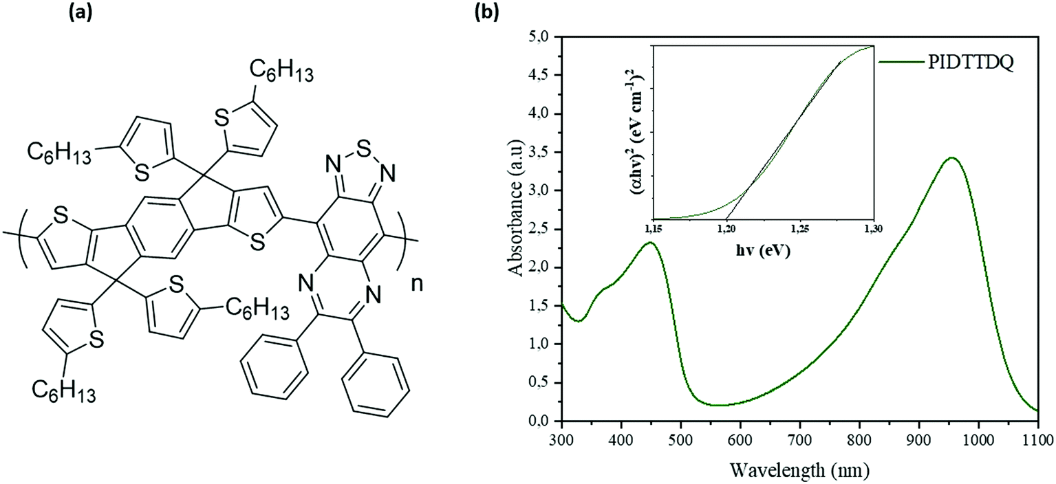
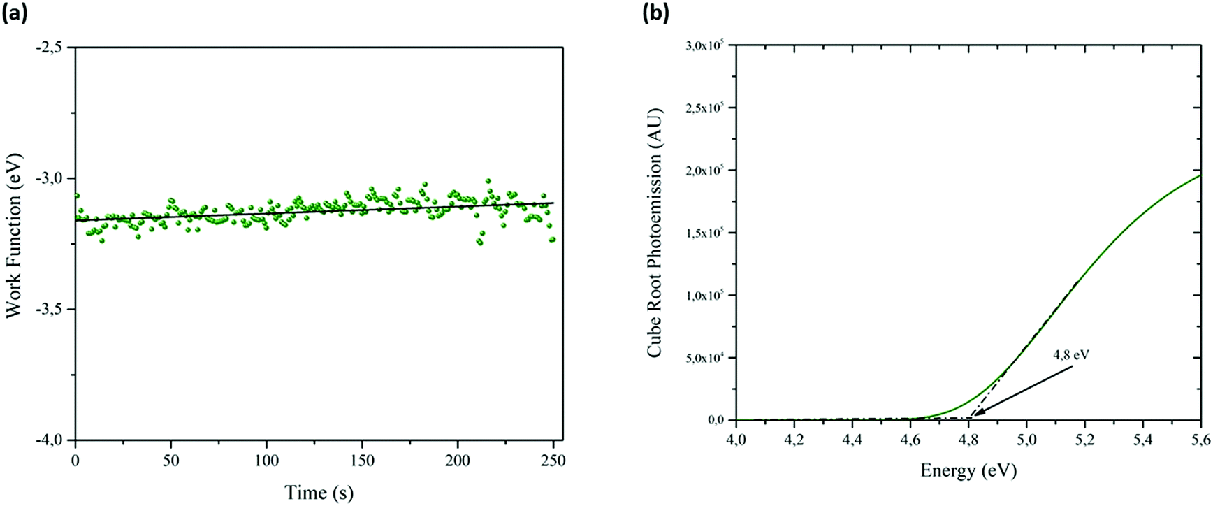
The chemical structure of the as synthesized PIDTTDQ Conjugated polymer is presented in Fig. 1a. Fig. S1 (ESI†) displays the 1H NMR spectrum of PIDTTDQ. More details about the synthetic procedures of PIDTTDQ can be found in the ESI.† In inverted PSCs, light enters the device from the HTL side, therefore, ideally, the HTL should not absorb light to reduce optical losses in the complete device. The Transmittance spectra of PIDTTDQ and PEDOT:PSS films on Glass/ITO were recorded for a thickness of ≈50nm. The results from the Transmittance spectra (Fig. S2, ESI†) show that PIDTTDQ is more transparent compared to PEDOT:PSS. The absorbance spectrum (Fig. 1b) of PIDTTDQ revealed two peaks in the visible and the IR range. The bandgap of PIDTTQ was estimated by using the Tauc plot method. The obtained bandgap was 1.2 eV. The Work Function (WF) and HOMO level of PIDTTDQ was then obtained by performing Kelvin Probe Force Microscopy (KPFM) and Ambient Photoemission spectroscopy (APS) measurements. We measured the work function of PIDTTDQ in neat films with a thickness of ≈50nm. Fig. 2a shows the measured WF as a function of time. The obtained WF was 3.16 ± 0.01 eV. This value remains stable over time with small fluctuations, showing the uniformity of PIDTTDQ thin films. We then estimated the valence band maximum (HOMO) using APS with a UV light source. Fig. 2b shows the Cube root photoemission as a function of energy. The HOMO level was estimated by extrapolating a straight line to the photoemission threshold. The obtained HOMO was −4.8 eV. Then, the LUMO value was extracted by combining the Uv-Vis and APS measurements. The calculated LUMO was −3.6 eV. The energy levels of PIDTTDQ are summarized in Table S1 (ESI†). The surface morphology of the HTL film is another crucial parameter to obtain efficient PSCs.40,41 The film morphology of the PIDTTDQ and PEDOT:PSS films on ITO was studied through Atomic Force Microscopy (AFM) imaging. The obtained film topography for a 5 × 5 μm image size is presented in Fig. S3a (ESI†) for PIDTTDQ and in Fig. S3b (ESI†) for PEDOT:PSS, where no major differences were observed between the topography of the two films. The Root Mean Square (RMS) roughness for PIDTTDQ and PEDOT:PSS was 2.3 and 1.6 nm respectively, showing a smooth morphology for both layers. The film morphology of the perovskite film was also studied, with PEDOT:PSS and PIDTTDQ as bottom layers, with the film topography presented in Fig. S3c and d (ESI†) respectively for a 5 × 5 μm image size. The RMS roughness for PIDTTDQ and PEDOT:PSS deposited on top of the perovskite layer was 14.1 and 16.2 nm, respectively. This indicates that the interface between the perovskite film and the HTL is smoother for PIDTTDQ than PEDOT:PSS, with a possible reduction in the number of interfacial defects. The wetting properties of both HTLs were then examined through water contact angle measurements on Glass/ITO, where the contact angle for PEDOT:PSS was 26.2°, while the corresponding value for PIDTTDQ was 96.0° as seen in Fig. S4(a) and (b) (ESI†). This illustrates that PIDTTDQ is more hydrophobic, and therefore can be more water-resistant than PEDOT:PSS, preventing humidity penetration and promoting better crystal growth of the perovskite film. The growth of the perovskite layer on hydrophobic films is usually associated with larger grains, due to the suppression of the nucleation process.42 The hydrophobic nature of PIDTTDQ raises the concern of whether it is wetting to DMF and thus the perovskite layer. To answer this question, we performed contact angle measurements using DMF. The corresponding contact angles for PEDOT:PSS and PIDTTDQ were 12.4° and 20.4°, respectively, as shown from Fig. S4(c) and (d) (ESI†). From these data, we can deduce that PIDTTDQ is wetting to DMF, thus the perovskite film can be deposited on top of it. The results given above demonstrate the potential of PIDTTDQ to further extend the lifetime of PSC devices. A higher hole mobility of an HTL can lead to improved hole transport and collection.44 The hole mobility of both PEDOT:PSS and PIDTTDQ films was calculated by fabricating hole-only devices structured as ITO/PIDTTDQ/Au and ITO/PEDOT:PSS/Au respectively, and by fitting the Mott–Gurney law in Fig. S5 (ESI†) as:| | 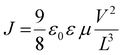 | (1) |
where J is the dark current density, V is the applied voltage, ε0 = 8.85 × 10⁻¹⁴ F cm−1 is the vacuum permittivity, ε ≈ 3 is the permittivity for an organic material, μ is the charge mobility and L ≈ 50nm is the film thickness. The calculated hole mobilities for PIDTTDQ and PEDOT:PSS were 2.35 × 10⁻⁴ and 2.56 × 10⁻⁴ cm2 V−1 s−1, indicating a similar transporting ability for the two HTLs.
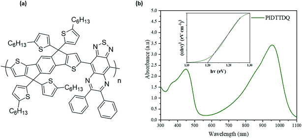 |
| | Fig. 1 (a) Chemical structure of the PIDTTDQ conjugated polymer (b) absorption spectrum of PIDTTDQ solution with obtained bandgap. | |
 |
| | Fig. 2 (a) PIDTTDQ work function measurement as a function of time (b) PIDTTDQ HOMO estimation using UV photoemission spectroscopy. | |
2.3 Device performance
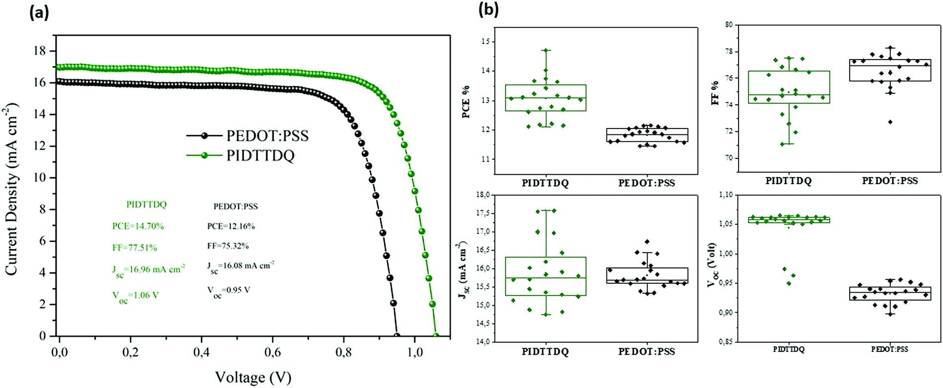
To further investigate the perovskite growth and device performance with the PIDTTDQ HTL, we fabricated p–i–n devices with the structure ITO/PIDTTDQ/Perovskite/PC60BM/BCP/Ag, as shown in Fig. S6a (ESI†). The device energy level diagram is shown in Fig. S6b (ESI†). The perovskite was based on the 4-cation composition Rb0.04Cs0.05(FA0.85MA0.15)0.91Pb(I0.85Br0.15)3 (referred to as RbCsFAMA), where the addition of RbI and CsI provides high efficiencies, better stability, and improved reproducibility.43,44 The thickness of the PIDTTDQ layer was optimized by testing various concentrations, namely 0.01, 0.05, 0.1, and 0.2 mg ml−1, and comparing the device performance. PIDTTDQ films exhibited a hydrophobic behavior when depositing the perovskite film on top of them. Intermediate concentration values were also investigated, however the obtained PCE values were inferior compared to the four concentration values mentioned previously. Since the Perovskite film growth on hydrophobic surfaces is a key issue and a significant consideration for large-area devices,45 we tried treating the PEDOT:PSS and PIDTTDQ films with DMF, before the perovskite deposition, but the treatment did not improve the perovskite film quality. The obtained photovoltaic parameters of the best device from each PIDTTDQ concentration with average values can be seen in Table S2 (ESI†). For concentrations of 0.01, 0.05, 0.1 and 0.2 mg ml−1, the best devices showed a PCE of 13.77%, 14.70%, 13.97%, and 12.60% respectively. A statistical comparison between each concentration is provided in Fig. S7 (ESI†), with box plots for each photovoltaic parameter. Based on the above, we concluded that a PIDTTDQ solution concentration of 0.05mg ml−1 yields the highest PCE and is the optimum concentration among all tested. We will refer to the devices with this optimized thickness for the rest of the study as PIDTTDQ. The performance of the PIDTTDQ HTL was then compared with the PEDOT:PSS reference device. Fig. 3a shows the J–V characteristic curves for both champion devices obtained with the two HTLs.
 |
| | Fig. 3 (a) J–V Curves of champion devices for PIDTTDQ and reference. (b) Box plots for photovoltaic parameters of 20 PIDTTDQ and PEDOT:PSS reference devices. | |
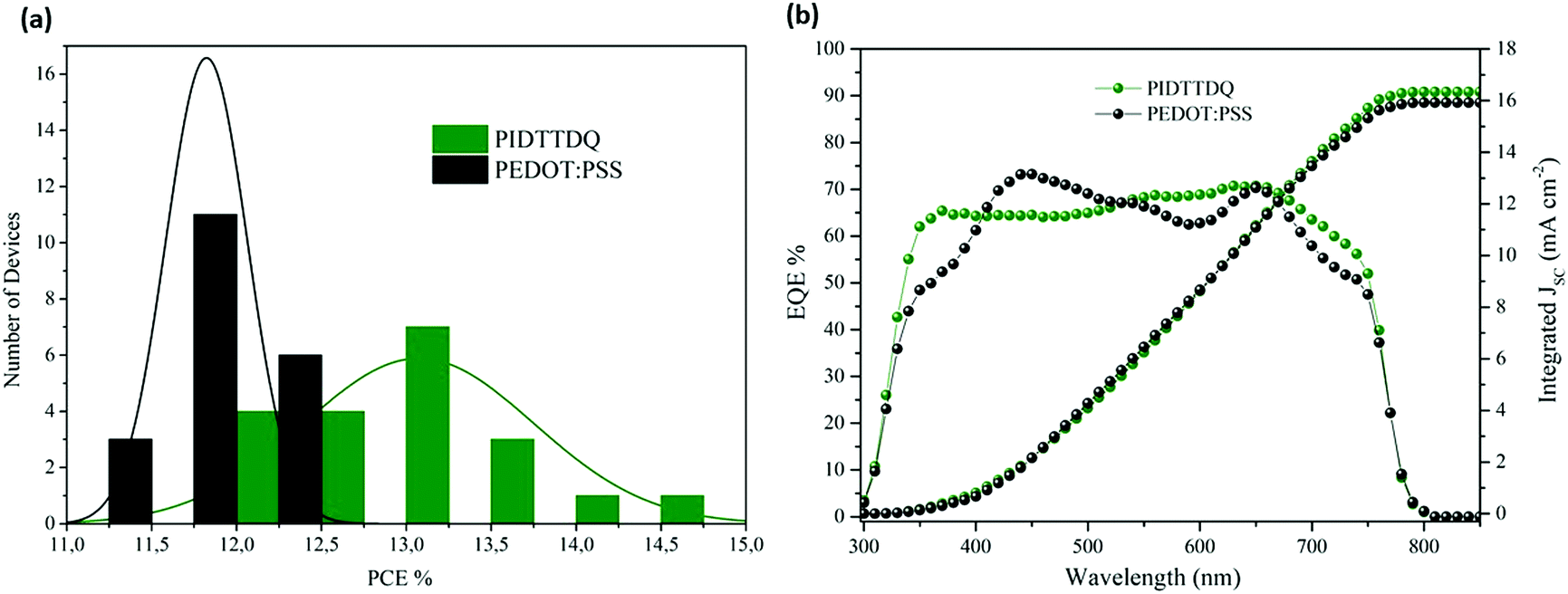
According to Table 1, the champion reference device showed a PCE of 12.16%, a Voc of 0.95V, a FF of 75.32%, and a JSC of 16.08 mA cm−2, compared to the PIDTTDQ champion device that has a PCE of 14.70%, Voc of 1.06V, FF of 77.51% and a JSC of 16.97 mA cm−2. PIDTTDQ exhibited a Voc increase of 110 mV. This increase might arise from the improved HTL/Perovskite interface and the reduced non-radiative interfacial recombination. Afterwards, we investigated the reproducibility of the devices. The results are presented as box plots with all the photovoltaic parameters for the 20 fabricated devices with PEDOT:PSS and PIDTTDQ in Fig. 3b. All obtained photovoltaic parameters for each of the 20 reference and PIDTTDQ devices are shown in Tables S3 and S4 (ESI†) respectively. Based on Table 1, the reference devices had on average a PCE of 11.82%, a Voc of 0.93V, a FF of 76.56%, and a JSC of 15.82 mA cm−2, while PIDTTDQ devices showed on average PCE of 13.07%, a Voc of 1.04V, a FF of 74.96% and a JSC of 15.88 mA cm−2. This data confirms the improved performance of PIDTTDQ with a 1.25% increase in PCE on average and a 110 mV increase in Voc. The improvement in device efficiency is also illustrated in the PCE histogram in Fig. 4a. To verify the current density obtained from the solar simulator, we then performed External Quantum Efficiency (EQE) measurements for both the PIDTTDQ and PEDOT: PSS devices, the results of which are presented in Fig. 4b. The integrated current density values for PIDTTDQ and PEDOT:PSS were 16.34 and 15.93 mA cm−2 respectively, which were virtually in agreement with the calculated JSC from the solar simulator. On average, the Jsc is almost identical for both devices. The average FF was 1.6% less for PIDTTDQ compared to PEDOT:PSS. The reason behind this difference lies at the conductivity of PIDTTDQ. We performed conductivity measurements on 50nm thick films of PIDTTDQ and PEDOT: PSS, on a diode configuration of ITO/HTL/Au. The results are presented in Fig. S8 (ESI†). The calculated conductivity of PIDTDDQ and PEDOT: PSS is 2.88 and 3.11 mS cm−1, respectively. Table S5 (ESI†) displays the series resistance values for 20 fabricated devices using PIDTTDQ and PEDOT: PSS. The average series resistance was 5.81 for PIDTTDQ and 5.28 for PEDOT:PSS. The low conductivity and higher series resistance of PIDTTDQ compared to PEDOT: PSS is the main cause for the reduced FF that PIDTTDQ devices exhibited. The lower hole mobiIity of PIDTTDQ compared to PEDOT:PSS can also harm the FF.46
Table 1 Photovoltaic Parameters of 20 fabricated devices for each case. The errors are calculated from device statistics. The brackets correspond to the champion devices
|
|
PCE % |
FF % |
J
SC (mA cm−2) |
Voc (V) |
| Reference |
11.82 ± 0.24 (12.16) |
76.56 ± 1.29 (75.32) |
15.82 ± 0.38 (16.08) |
0.93 ± 0.02 (0.95) |
| PIDTTDQ |
13.07 ± 0.68 (14.70) |
74.96 ± 1.83 (77.51) |
15.88 ± 0.85 (16.97) |
1.04 ± 0.04 (1.06) |
 |
| | Fig. 4 (a) Statistical distribution of PCE for 20 fabricated devices using PEDOT:PSS and PIDTTDQ. (b) EQE Spectrum for PIDTTDQ and PEDOT:PSS devices. | |
2.4 Optoelectronic characterization
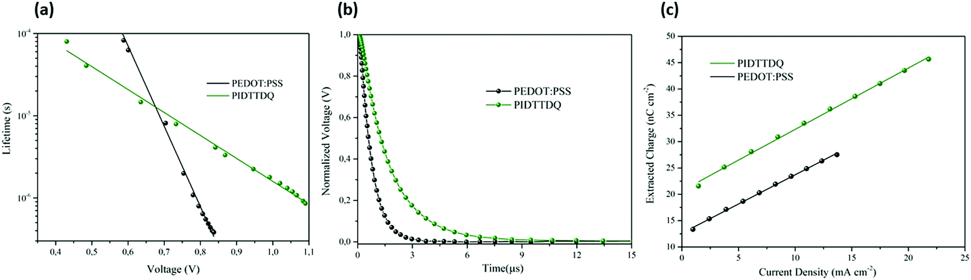
To investigate the mechanism responsible for the Voc and the PCE enhancement after introducing the PIDTTDQ HTL, we performed Transient Photovoltage (TPV) and Transient Photocurrent (TPC) measurements for various light intensities (Fig. S9 and S10, ESI†). The objective of these measurements was to interpret the device performance enhancement by studying the charge recombination and extraction at the HTL/perovskite interface. For TPV and TPC measurements, the devices are held in an open-circuit and short-circuit by connecting them with a 1MΩ and a 50Ω resistor, respectively. The TPV measurements are performed under a small perturbation to ensure a single exponential decay. The limitations in Voc arise from non-radiative recombination losses at the interfaces.47 Suppressing interface recombination can lead to Voc values closer to the thermodynamic limit.48 The observed Voc < 1 V for the reference devices with PEDOT:PSS is due to the holes being close at the PEDOT:PSS/perovskite interface and the insufficient electron blocking. Surface Recombination effects and leakage currents have both been observed in PSCs using PEDOT:PSS as the HTL.49Fig. 5a shows the obtained lifetime from the TPV as a function of bias. We observe that as bias increases, the decay of carrier lifetime is rapid for PEDOT:PSS compared to PIDTTDQ. We therefore conclude that PIDTTDQ has slower recombination dynamics and prevents interfacial recombination more effectively compared to PEDOT:PSS, confirming the formation of a better HTL/perovskite interface.50Fig. 5b shows the normalized TPV decays under the same illumination for both devices. The calculated carrier lifetime for PIDTTDQ and PEDOT:PSS by fitting a first-order exponential decay was 1.78 μs and 0.8 μs respectively, corroborating the improved carrier lifetime for PIDTTDQ devices. The extracted charge from the TPC measurements was plotted as a function of current density, as seen in Fig. 5c. The PIDTTDQ HTL improves the charge collection compared to PEDOT:PSS. Combining the findings from both TPC and TPV measurements, we can confidently report an improved carrier lifetime and charge collection for the case of the PIDTTDQ HTL.
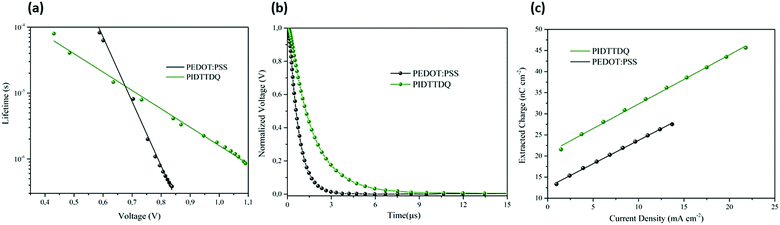 |
| | Fig. 5 (a) Lifetime obtained from TPV measurement as a function of voltage. (b) Normalized transient photovoltage decays under the same illumination for PIDTTDQ and reference device. (c) extracted charge density from TPC measurement as a function of current Density. | |
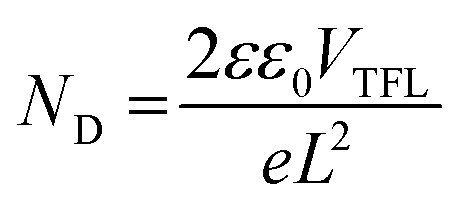
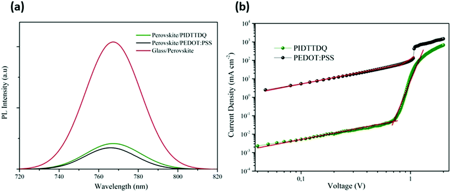
The charge transport and recombination were further studied through steady-state photoluminescence (PL) measurements. The PL spectra for the bare perovskite film and with perovskite on top of the PIDTTDQ and PEDOT:PSS layers are shown in Fig. 6a. All PL emission peaks appear at 770nm, as expected.43 The PL peak is attributed to the radiative band-to-band recombination. It is evident that the PL intensity is quenched when perovskite films are deposited on top of the PEDOT:PSS and PIDTTDQ layers, where the obtained quenching is due to the efficient charge transfer at the HTL/Perovskite interface.51–54 We then measured the dark J–V characteristics of hole-only devices for PIDTTDQ and PEDOT:PSS using the configuration HTL/Perovskite/PTAA/Au to estimate the defect density of the perovskite layer. The defect density for each case is calculated through the SCLC technique (Fig. 6b). The J–V plot in Fig. 6b is separated into three regions: In the first region the current increases linearly with voltage (Linear region), in the second region the current increases abruptly with a slope larger than 3, which is the trap filling region (TFL) and in the third region the slope is equal to 2 (Child region). The transition from the linear to the Trap Filling Region occurs at a certain voltage, the trap filling voltage VTFL. The defect density is then calculated through the equation
| |  | (2) |
where
ε0 = 8.85 × 10
−14 F cm
−1 is the vacuum permittivity,
ε = 46.9 is the perovskite permittivity,
e is the elementary charge and
L ≈ 450 nm is the thickness of the perovskite active layer.
55,56 The calculated
VTFL of PIDTTDQ and PEDOT:PSS is 0.70 V and 0.83 V, and the respective defect densities are 1.79 × 10
16 cm
−3 and 2.12 × 10
16 cm
−3. The higher defect density calculated for PEDOT:PSS supplements the passivation effect of PIDTTDQ on the perovskite film. In addition, the increased
J0 by almost 3 orders of magnitude indicates increased leakage current and recombination for the case of PEDOT:PSS devices.
56
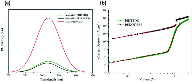 |
| | Fig. 6 (a) Steady state photoluminescence (PL). (b) Dark J–V characteristics of hole-only devices. | |
2.5 Device stability
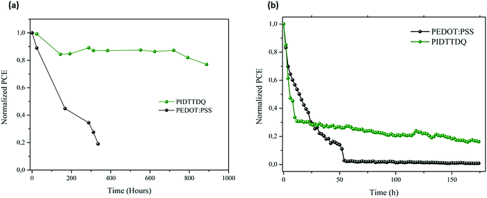
The device stability for both PIDTTDQ and PEDOT:PSS reference device was evaluated by performing the ISOS D1 and ISOS L2 protocols. For the ISOS D1 test, unencapsulated devices were stored in ambient air in the dark, with ambient humidity ranging between 50–70%. The results are shown in Fig. 7a, where the normalized PCE is plotted as a function of exposure time. The degradation of PEDOT:PSS reference device is evident, as the device lasts for less than 400 h of exposure. The rapid degradation is due to the hydrophilic nature of the material. On the opposite, PIDTTDQ devices maintained more than 75% of the initial PCE after almost 900 h. The improved moisture stability can be attributed to the hydrophobic nature of the material, which serves as a protection layer and slows down the decomposition rate of the perovskite absorber. To further investigate the device stability, the ISOS L2 protocol was implemented. In this case, encapsulated devices are stored inside an environmental chamber under continuous 1sun illumination at an elevated temperature of above 65 °C, under humidity that does not exceed 15%. Then, the PCE is monitored as a function of exposure time by using the chamber's solar simulator. The results are summarized in Fig. 7b. The PIDTTDQ device entered a burn-in phase that lasted for about 10 h. Then, the device PCE dropped to the 20% of its initial value after almost 80 h, which corresponds to the TS80 lifetime.57 In contrast, the PEDOT:PSS device did not recover from the burn-in phase and the device degraded completely after approximately 50 h. These data verify the improved thermal, light, and moisture stability of the PIDTDDQ device. Solar cell stability is a critical issue for the commercialization of PSCs.
 |
| | Fig. 7 (a)Device stability evaluation using the ISOS D1 Protocol. (b) Device lifetime investigation using the ISOS L2 protocol. | |
3. Conclusions
In summary, we investigated the performance of the novel, hydrophobic conjugated polymer PIDTTDQ as the hole transport layer in inverted PSCs. After optimization, the optimal thickness for PIDTTDQ was obtained at a concentration of 0.05 mg ml−1 and the best device for PIDTTDQ yielded a PCE of 14.70%, compared to the reference device with PEDOT:PSS which exhibited an optimal PCE of 12.16%. The device characterization revealed increased interfacial recombination for PEDOT: PSS, in addition to the reduced number of defects of the perovskite layer. The device stability was investigated using ISOS protocols. The results demonstrated an improved moisture, light and thermal stability for PIDTTDQ. This novel polymer has the potential by further molecular engineering to extend its application and promote its incorporation into large area devices.
Conflicts of interest
There are no conflicts to declare.
Acknowledgements
This research has been co-financed by the European Union and Greek national funds through the Operational Program Competitiveness, Entrepreneurship, and Innovation, under the call RESEARCH – CREATE – INNOVATE (project code: T1EDK-01082).
References
- A. Kojima, K. Teshima, Y. Shirai and T. Miyasaka, J. Am. Chem. Soc., 2009, 131, 6050–6051, DOI:10.1021/ja809598r.
- J. J. Yoo, G. Seo, M. R. Chua, T. G. Park, Y. Lu, F. Rotermund, Y. K. Kim, C. S. Moon, N. J. Jeon, J. P. Correa-Baena, V. Bulović, S. S. Shin, M. G. Bawendi and J. Seo, Nature, 2021, 590, 587–593, DOI:10.1038/s41586-021-03285-w.
- J. Y. Kim, J. W. Lee, H. S. Jung, H. Shin and N. G. Park, Chem. Rev., 2020, 120(15), 7867–7918, DOI:10.1021/acs.chemrev.0c00107.
- J. Jeong, M. Kim, J. Seo, H. Lu, P. Ahlawat, A. Mishra, Y. Yang, M. A. Hope, F. T. Eickemeyer, M. Kim, Y. J. Yoon, I. W. Choi, B. P. Darwich, S. J. Choi, Y. Jo, J. H. Lee, B. Walker, S. M. Zakeeruddin, L. Emsley, U. Rothlisberger, A. Hagfeldt, D. S. Kim, M. Grätzel and J. Y. Kim, Nature, 2021, 592, 381–385, DOI:10.1038/s41586-021-03406-5.
- NREL, https://www.nrel.gov/pv/cell-efficiency.html.
- X. Zheng, Y. Hou, C. Bao, J. Yin, F. Yuan, Z. Huang, K. Song, J. Liu, J. Troughton, N. Gasparini, C. Zhou, Y. Lin, D. J. Xue, B. Chen, A. K. Johnston, N. Wei, M. N. Hedhili, M. Wei, A. Y. Alsalloum, P. Maity, B. Turedi, C. Yang, D. Baran, T. D. Anthopoulos, Y. Han, Z. H. Lu, O. F. Mohammed, F. Gao, E. H. Sargent and O. M. Bakr, Nat. Energy, 2020, 5, 131–140, DOI:10.1038/s41560-019-0538-4.
- S. Wu, J. Zhang, Z. Li, D. Liu, M. Qin, S. H. Cheung, X. Lu, D. Lei, S. K. So, Z. Zhu and A. K. Y. Jen, Joule, 2020, 4(6), 1248–1262, DOI:10.1016/j.joule.2020.04.001.
- F. Li, X. Deng, F. Qi, Z. Li, D. Liu, D. Shen, M. Qin, S. Wu, F. Lin, S. H. Jang, J. Zhang, X. Lu, D. Lei, C. S. Lee, Z. Zhu and A. K. Y. Jen, J. Am. Chem. Soc., 2020, 47(142), 20134–20142, DOI:10.1021/jacs.0c09845.
- A. Y. Alsalloum, B. Turedi, X. Zheng, S. Mitra, A. A. Zhumekenov, K. J. Lee, P. Maity, I. Gereige, A. AlSaggaf, I. S. Roqan, O. F. Mohammed and O. M. Bakr, ACS Energy Lett., 2020, 5, 657–662, DOI:10.1021/acsenergylett.9b02787.
- T. Liu, K. Chen, Q. Hu, R. Zhu and Q. Gong, Adv. Energy Mater., 2016, 6(17) DOI:10.1002/aenm.201600457.
- C. Polyzoidis, K. Rogdakis and E. Kymakis, Adv. Energy Mater., 2021, 2101854, DOI:10.1002/aenm.202101854.
- D. H. Kang and N. G. Park, Adv. Mater., 2019, 31(34) DOI:10.1002/adma.201805214.
- A. Al-Ashouri, E. Köhnen, B. Li, A. Magomedov, H. Hempel, P. Caprioglio, J. A. Márquez, A. B. M. Vilches, E. Kasparavicius, J. A. Smith, N. Phung, D. Menzel, M. Grischek, L. Kegelmann, D. Skroblin, C. Gollwitzer, T. Malinauskas, M. Jošt, G. Matič, B. Rech, R. Schlatmann, M. Topič, L. Korte, A. Abate, B. Stannowski, D. Neher, M. Stolterfoht, T. Unold, V. Getautis and S. Albrecht, Science, 2020, 370(6522), 1300–1309, DOI:10.1126/science.abd4016.
- Z. Zhang, M. Sheri, Z. A. Page, T. Emrick, A. Saeki, Y. Liu and T. P. Russell, ACS Appl. Mater. Interfaces, 2020, 12(50), 56068–56075, DOI:10.1021/acsami.0c18108.
- M. Stolterfoht, P. Caprioglio, C. M. Wolff, J. A. Márquez, J. Nordmann, S. Zhang, D. Rothhardt, U. Hörmann, Y. Amir, A. Redinger, L. Kegelmann, F. Zu, S. Albrecht, N. Koch, T. Kirchartz, M. Saliba, T. Unold and D. Neher, Energy Environ. Sci., 2019, 12(9), 2778–2788, 10.1039/c9ee02020a.
- L. Meng, J. You, T. F. Guo and Y. Yang, Acc. Chem. Res., 2016, 49, 155–165, DOI:10.1021/acs.accounts.5b00404.
- M. Bidikoudi and E. Kymakis, J. Mater. Chem. C, 2019, 7, 13680–13708, 10.1039/C9TC04009A.
- X. Fan, W. Nie, H. Tsai, N. Wang, H. Huang, Y. Cheng, R. Wen, L. Ma, F. Yan and Y. Xia, Adv. Sci., 2019, 6(19), 1900813, DOI:10.1002/advs.201900813.
- W. Han, G. Ren, J. Liu, Z. Li, H. Bao, C. Liu and W. Guo, ACS Appl. Mater. Interfaces, 2020, 12(44), 49297–49322, DOI:10.1021/acsami.0c13576.
- S. M. Kim, C. H. Kim, Y. Kim, N. Kim, W. J. Lee, E. H. Lee, D. Kim, S. Park, K. Lee, J. Rivnay and M. H. Yoon, Nat. Commun., 2018, 9(1), 1–9, DOI:10.1038/s41467-018-06084-6.
- C. Bracher, B. G. Freestone, D. K. Mohamad, J. A. Smith and D. G. Lidzey, Energy Sci. Eng., 2018, 6(1), 35–46, DOI:10.1002/ese3.180.
- L. Hu, K. Sun, M. Wang, W. Chen, B. Yang, J. Fu, Z. Xiong, X. Li, X. Tang, Z. Zang, S. Zhang, L. Sun and M. Li, ACS Appl. Mater. Interfaces, 2017, 9(50), 43902–43909, DOI:10.1021/acsami.7b14592.
- X. Liu, B. Li, N. Zhang, Z. Yu, K. Sun, B. Tang, D. Shi, H. Yao, J. Ouyang and H. Gong, Nano Energy, 2018, 53, 567–578, DOI:10.1016/j.nanoen.2018.09.023.
- K. Jiang, F. Wu, G. Zhang, P. C. Y. Chow, C. Ma, S. Li, K. S. Wong, L. Zhu and H. Yan, J. Mater. Chem. A, 2019, 7(38), 21662–21667, 10.1039/c9ta08995k.
- Q. Wang, C. C. Chueh, M. Eslamian and A. K. Y. Jen, ACS Appl. Mater. Interfaces, 2016, 8(46), 32068–32076, DOI:10.1021/acsami.6b11757.
- K. M. Reza, A. Gurung, B. Bahrami, S. Mabrouk, H. Elbohy, R. Pathak, K. Chen, A. H. Chowdhury, M. T. Rahman, S. Letourneau, H. C. Yang, G. Saianand, J. W. Elam, S. B. Darling and Q. Qiao, J. Energy Chem., 2020, 44, 41–50, DOI:10.1016/j.jechem.2019.09.014.
- Z. Hawash, L. K. Ono and Y. Qi, Adv. Mater. Interfaces, 2018, 5(1), 1700623, DOI:10.1002/admi.201700623.
- A. Al-Ashouri, A. Magomedov, M. Roß, M. Jošt, M. Talaikis, G. Chistiakova, T. Bertram, J. A. Márquez, E. Köhnen, E. Kasparavičius, S. Levcenco, L. Gil-Escrig, C. J. Hages, R. Schlatmann, B. Rech, T. Malinauskas, T. Unold, C. A. Kaufmann, L. Korte, G. Niaura, V. Getautis and S. Albrecht, Energy Environ. Sci., 2019, 12, 3356–3369, 10.1039/C9EE02268F.
- P. H. Liu, C. H. Chuang, Y. L. Zhou, S. H. Wang, R. J. Jeng, S. P. Rwei, W. Bin Liau and L. Wang, J. Mater. Chem. A, 2020, 8(47), 25173–25177, 10.1039/d0ta09063h.
- G. Grancini, C. Roldán-Carmona, I. Zimmermann, E. Mosconi, X. Lee, D. Martineau, S. Narbey, F. Oswald, F. De Angelis, M. Graetzel and M. K. Nazeeruddin, Nat. Commun., 2017, 8(1), 1–8, DOI:10.1038/ncomms15684.
- L. Meng, J. You and Y. Yang, Nat. Commun., 2018, 9(1), 1–4, DOI:10.1038/s41467-018-07255-1.
- D. C. Jordan, T. J. Silverman, J. H. Wohlgemuth, S. R. Kurtz and K. T. VanSant, Prog. Photovoltaics Res. Appl., 2017, 25(4), 318–326, DOI:10.1002/pip.2866.
- P. Holzhey and M. Saliba, J. Mater. Chem. A, 2018, 6(44), 21794–21808, 10.1039/C8TA06950F.
- R. Wang, M. Mujahid, Y. Duan, Z. K. Wang, J. Xue and Y. Yang, Adv. Funct. Mater., 2019, 29(47), 1808843, DOI:10.1002/adfm.201808843.
- B. Roose, Q. Wang and A. Abate, Adv. Energy Mater., 2019, 9(5), 1803140, DOI:10.1002/aenm.201803140.
- J. J. Lee, S. H. Lee, F. S. Kim, H. H. Choi and J. H. Kim, Org. Electron., 2015, 26, 191–199, DOI:10.1016/j.orgel.2015.07.022.
- J. M. Yun, J. S. Yeo, J. Kim, H. G. Jeong, D. Y. Kim, Y. J. Noh, S. S. Kim, B. C. Ku and S. I. Na, Adv. Mater., 2011, 23(42), 4923–4928, DOI:10.1002/adma.201102207.
- S. Ma, W. Qiao, T. Cheng, B. Zhang, J. Yao, A. Alsaedi, T. Hayat, Y. Ding, Z. Tan and S. Dai, ACS Appl. Mater. Interfaces, 2018, 10(4), 3902–3911, DOI:10.1021/acsami.7b19053.
- D. S. Mann, Y. H. Seo, S. N. Kwon and S. I. Na, J. Alloys Compd., 2020, 812, 152091, DOI:10.1016/j.jallcom.2019.152091.
- H. Elbohy, B. Bahrami, S. Mabrouk, K. M. Reza, A. Gurung, R. Pathak, M. Liang, Q. Qiao and K. Zhu, Adv. Funct. Mater., 2019, 29(47), 1806740, DOI:10.1002/adfm.201806740.
- X. Zhou, M. Hu, C. Liu, L. Zhang, X. Zhong, X. Li, Y. Tian, C. Cheng and B. Xu, Nano Energy, 2019, 63, 103866, DOI:10.1016/j.nanoen.2019.103866.
- C. Bi, Q. Wang, Y. Shao, Y. Yuan, Z. Xiao and J. Huang, Nat. Commun., 2015, 6(1), 1–7, DOI:10.1038/ncomms8747.
- M. Saliba, T. Matsui, K. Domanski, J. Y. Seo, A. Ummadisingu, S. M. Zakeeruddin, J. P. Correa-Baena, W. R. Tress, A. Abate, A. Hagfeldt and M. Grätzel, Science, 2016, 354(6309), 206–209, DOI:10.1126/science.aah5557.
- M. Saliba, T. Matsui, J. Y. Seo, K. Domanski, J. P. Correa-Baena, M. K. Nazeeruddin, S. M. Zakeeruddin, W. Tress, A. Abate, A. Hagfeldt and M. Grätzel, Energy Environ. Sci., 2016, 9, 1989–1997, 10.1039/C5EE03874J.
- F. H. Isikgor, A. S. Subbiah, M. K. Eswaran, C. T. Howells, A. Babayigit, M. De Bastiani, E. Yengel, J. Liu, F. Furlan, G. T. Harrison, S. Zhumagali, J. I. Khan, F. Laquai, T. D. Anthopoulos, I. McCulloch, U. Schwingenschlögl and S. De Wolf, Nano Energy, 2021, 81, 105633, DOI:10.1016/j.nanoen.2020.105633.
- M. Stolterfoht, C. M. Wolff, Y. Amir, A. Paulke, L. Perdigón-Toro, P. Caprioglio and D. Neher, Energy Environ. Sci., 2017, 10, 1530–1539, 10.1039/C7EE00899F.
- N. Yaghoobi Nia, M. Méndez, B. Paci, A. Generosi, A. Di Carlo and E. Palomares, ACS Appl. Energy Mater., 2020, 3, 6853–6859, DOI:10.1021/acsaem.0c00956.
- M. Stolterfoht, C. M. Wolff, J. A. Márquez, S. Zhang, C. J. Hages, D. Rothhardt, S. Albrecht, P. L. Burn, P. Meredith, T. Unold and D. Neher, Nat. Energy, 2018, 3(10), 847–854, DOI:10.1038/s41560-018-0219-8.
- J. P. Correa-Baena, W. Tress, K. Domanski, E. H. Anaraki, S. H. Turren-Cruz, B. Roose, P. P. Boix, M. Grätzel, M. Saliba, A. Abate and A. Hagfeldt, Energy Environ. Sci., 2017, 10(5), 1207–1212, 10.1039/c7ee00421d.
- K. Tvingstedt, L. Gil-Escrig, C. Momblona, P. Rieder, D. Kiermasch, M. Sessolo, A. Baumann, H. J. Bolink and V. Dyakonov, ACS Energy Lett., 2017, 2(2), 424–430, DOI:10.1021/acsenergylett.6b00719.
- J. Liu, W. Liu, E. Aydin, G. T. Harrison, F. H. Isikgor, X. Yang, A. S. Subbiah and S. De Wolf, ACS Appl. Mater. Interfaces, 2020, 12(21), 23874–23884, DOI:10.1021/acsami.0c03660.
- B. Xu, J. Zhang, Y. Hua, P. Liu, L. Wang, C. Ruan, Y. Li, G. Boschloo, E. M. J. Johansson, L. Kloo, A. Hagfeldt, A. K. Y. Jen and L. Sun, Chem, 2017, 2(5), 676–687, DOI:10.1016/j.chempr.2017.03.011.
- W. Budiawan, K. W. Lai, P. Karuppuswamy, T. S. Jadhav, Y. A. Lu, K. C. Ho, P. C. Wang, C. C. Chang and C. W. Chu, ACS Appl. Mater. Interfaces, 2020, 12(26) DOI:10.1021/acsami.0c02204.
- W. Zhang, L. Wan, S. Fu, X. Li and J. Fang, J. Mater. Chem. A, 2020, 8(14), 6546–6554, 10.1039/d0ta01860k.
- M. Petrović, T. Maksudov, A. Panagiotopoulos, E. Serpetzoglou, I. Konidakis, M. M. Stylianakis, E. Stratakis and E. Kymakis, Nanoscale Adv., 2019, 1(8), 3107–3118, 10.1039/c9na00246d.
- R. Li, P. Wang, B. Chen, X. Cui, Y. Ding, Y. Li, D. Zhang, Y. Zhao and X. Zhang, ACS Energy Lett., 2019, 5(1), 79–86, DOI:10.1021/acsenergylett.9b02112.
- K. Chatzimanolis, K. Rogdakis, D. Tsikritzis, N. Tzoganakis, M. Tountas, M. Krassas, S. Bellani, L. Najafi, B. Martín-García, R. Oropesa-Nuñez, M. Prato, G. Bianca, I. Plutnarova, Z. Sofer, F. Bonaccorso and E. Kymakis, Nanoscale Adv., 2021, 3, 3124–3135, 10.1039/D1NA00172H.
|
| This journal is © The Royal Society of Chemistry 2022 |

 Open Access Article
 This Open Access Article is licensed under a Creative Commons Attribution-Non Commercial 3.0 Unported Licence
 bc,
Alkmini
Nega
bd,
Andriana
Schiza
b,
Christos
Polyzoidis
a,
Vasilis G.
Gregoriou
ce and
Emmanuel
Kymakis
bc,
Alkmini
Nega
bd,
Andriana
Schiza
b,
Christos
Polyzoidis
a,
Vasilis G.
Gregoriou
ce and
Emmanuel
Kymakis