
 Open Access Article
 This Open Access Article is licensed under a
 Creative Commons Attribution 3.0 Unported Licence
Low-temperature annealed methylammonium-free perovskites prepared under ambient conditions in C electrode-based perovskite solar cells†
Maria
Bidikoudi
*a,
Vassilios
Dracopoulos
b and
Elias
Stathatos
 *a
*a
aNanotechnology and Advanced Materials Laboratory, Department of Electrical and Computer Engineering, University of the Peloponnese, 26334 Patras, Greece. E-mail: mbidikoudi@uop.gr; estathatos@uop.gr
bFoundation for Research & Technology, HELLAS (FORTH), Institute of Chemical Engineering Sciences (ICE-HT), Platani Rio, 1414, Patras, Greece
First published on 14th January 2022
Abstract
A study of the optimization of methylammonium (MA) free perovskite compositions, targeted for their application in hole transport layer (HTL) free perovskite solar cells with a carbon electrode (C-PSCs), is presented. Initially, through the evaluation of cesium and rubidium inorganic cations or mixtures of them used to stabilize the formamidinium (FA) based FAPbI3 perovskite to the black, active phase, cesium (Cs) has emerged as highly promising. Further optimization of the perovskite composition by fine-tuning the Cs/FA ratio has enabled C-PSCs with power conversion efficiencies (PCE) exceeding 12%. The C-PSCs present high photocurrent density and FF values, owing to the optimal crystallization, absorption ability and charge transfer properties, which have been confirmed using spectroscopy methods. Moreover, MA-free C-PSCs have been prepared entirely under ambient conditions, using low cost and low perovskite annealing methods, highlighting the potential of FA based perovskites for large area applications and contributing to the path towards their commercialization.
Introduction
After more than 10 years of intensive research in the field of perovskite solar cells, advances in chemical compositions, material tailoring and device engineering have enabled solar cells that demonstrate a certified power conversion efficiency (PCE) exceeding 25%,1 in devices with a typical electron transport layer (ETL)/perovskite/hole transporting layer (HTL)/metal electrode structure, of either the normal or inverted configuration. However, an alternative type of PSC has shown a notable increase in the scientific literature during the last 5 years. These are the PSCs where a counter electrode (CE), typically deposited on the devices at the last stage of their fabrication by thermal evaporation of a metal, such as Ag and Au, is prepared using a low-cost carbon (C) paste and these are referred to as carbon based PSCs (C-PSCs). By replacing the metal electrode with a C electrode, apart from the obvious advantage of cost reduction, the problems that are associated with the metals, such as ion migration and corrosion,2–5 which penalize the stability of the devices, are eliminated. Among the device architectures of C-PSCs, the one that presents a particular interest is the triple mesoscopic structure, which comprises a mesoporous oxide layer serving as the ETL (e.g. TiO2), a mesoporous insulating layer (e.g. ZrO2) and a mesoporous C electrode. The perovskite is infiltrated through the triple layer stack and crystallized after annealing. This device architecture possesses some very promising features, including the ability to be prepared under ambient conditions and the ability to function without a HTL, by exploiting the hole transport capability of both the perovskite and C electrode. The aforementioned advantages over the typical PSC structure combined with the high stability that C-PSCs exhibit, make them ideal for application in large area devices and favor the leap from lab-scale solar cells to a commercially available product. For this reason, growing interest and intensive research in C-PSCs have achieved an increase in PCE values from 6.64%6 in their first report in 2013 to over 17%.7The most widely studied perovskites, which are able to deliver high PCE values, employ the methylammonium (MA) cation in single or mixed cations and single or mixed halide compositions. However, the bandgap of these perovskites, being >1.5 eV,8 is not ideal for solar cell applications, since it is higher than the Shockley–Quessier optimum bandgap of 1.2–1.45 eV,9 imposing a limitation to the maximum attainable PCE. Moreover, the MA cation's high hygroscopicity makes it unsuitable for ambient handling, while it is also thermally unstable, undergoing phase transitions from a tetragonal to a cubic phase above 55 °C and degrading above 85 °C, as well as upon exposure to moisture in the air, due to its low crystallization energy and volatile nature.10–12 The above features hinder the application of MA-based perovskites in large area, “realistic” devices. For this reason, the replacement of MA with the more stable formamidinium (FA) cation has been pursued and the turn to MA-free perovskite compositions is highly acknowledged.
FA-based perovskites are characterized by lower bandgap values, and consequently extended light harvesting ability, long charge diffusion length and high photostability.13–16 Even though these properties are highly desirable for solar cell applications, the single cation, single halide FAPbI3 perovskite requires a high temperature annealing in order to convert to the black phase, while it also converts back to the non-perovskite δ-phase at working temperatures.17 Therefore, it is crucial in order to take complete advantage of the FA cation's favourable properties, to use a mixed-cation approach, employing a secondary cation to the primary FA cation, as a stabilizing agent.
Herein, a study of the impact of inorganic cations as stabilizers of the FAPbI3 perovskite is presented. This work focuses on the preparation of FA-based perovskites under ambient conditions, using a low-temperature annealing process, and their incorporation in HTL-free, carbon electrode-based perovskite solar cells (C-PSCs) of the triple mesoscopic structure. The choice of both device architecture and fabrication method has been such that the outcomes are targeted to applications in ambient-processed PSCs and modules that can be fabricated using simple methods such as printing, with the potential to transfer this technology to the large scale, of which there are very few reports in the literature (Table S1, ESI†).
To this end, HTL-free, C-PSCs have been prepared under ambient conditions with no control over temperature, oxygen and humidity, implementing FA-based perovskites that have been crystallized at a low temperature (100 °C). Initially a scrutinizing process of the two inorganic cations of Rb+ and Cs+, as well as a combination of both, was performed and the effects of their incorporation in FAPbI3 C-PSCs have been studied using crystallography (XRD), voltammetry and spectroscopy (UV-vis and electrochemical impedance spectroscopy) methods. From this study, Cs has emerged as the most promising; hence, in the second step, the Cs content in perovskites of the CsxFA1−xPbI3 composition has been varied in order to determine the optimum Cs/FA ratio. The optimization process has yielded C-PSCs with a photocurrent density value higher than 24 mA cm−2, a Voc value exceeding 830 mV, a very promising FF value of over 0.6 and a final PCE of ∼12.2%, with high reproducibility.
On the one hand, the motivation behind this study is the uniqueness of the triple mesoscopic structure C-PSCs, which are HTL-free and metal electrode free, while the entire solar cell fabrication process is conducted under ambient conditions. On the other hand, we propose a low temperature and low-cost fabrication method that can be applied over a large area, towards the commercialization of this type of PSCs, which would implement a perovskite absorber with a bandgap close to the optimal for solar cell applications with a simultaneous elimination of the unstable MA-cation.
Results and discussion
1. Cation type investigation
The initial step for this study was to scrutinize the effects of different inorganic cations, as per their capability to stabilize the FAPbI3 perovskite, which is well known to require a high temperature annealing (150 °C) in order to form the active, black perovskite phase, while it is also prone to structural changes and conversion to the inactive α-phase when handled under ambient conditions. For this purpose, in the literature, the two most promising and widely adopted inorganic iodides rubidium iodide (RbI), cesium iodide (CsI) and a combination of both have been employed in the FAPbI3 perovskite precursor solution and the properties of the resulting perovskites, as well as the corresponding C-PSCs, have been studied. For simplicity reasons, the CsxRbyFA1−x−yPbI3 perovskite formulations are denoted as Rb10, Cs5Rb5 and Cs10, where x and y refer to the molar percentage of the inorganic cations employed. The % mol of the organic cation FA+ is set to 90 and kept stable.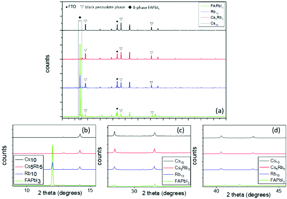 | ||
| Fig. 1 X-ray diffraction patterns of the perovskite films (a) at full range and (bottom) with a focus at 10–15° (b), 28–33° (c), and 42–46° (d). The “∇” denotes the perovskite peaks and “*” denotes the fluorine-doped tin oxide (FTO) peaks. | ||
By zooming in on the region between 10° and 15°, where the peaks of the inactive δ-phase of FAPbI3 and the first perovskite peak (100) appear, we notice a great difference among the spectra obtained, mainly regarding the photoinactive hexagonal δ-phase of the FAPbI3 peak, present at ∼11.7°.18–20 A very intense peak is recorded for the FAPbI3 perovskite, clearly indicating the incomplete formation of the FAPbI3 precursor to the black, active perovskite phase. This is an expected observation, since it is well known that FAPbI3 requires a high temperature annealing in order to form the active perovskite, in addition to being highly unstable under ambient conditions, which is the fabrication method employed in this study. This peak is noticeably reduced after Rb addition, with a further reduction after Cs addition and the complete elimination of the peak is observed after the replacement of Rb with Cs. This can be attributed to the ionic radius of Cs+ (1.81 Å), which is smaller than that of FA+ (2.79 Å),21 with this size difference promoting the fine-tuning of the Goldschmidt tolerance factor towards more structurally stable regions, as it has been previously reported in the literature.20,22,23 In contrast, the size of the Rb cation (1.64 Å)24 is too small, thus hindering the formation of the perovskite lattice and promoting the formation of non-perovskite side phases such as RbPb(I1−xBrx)3.25,26 This result predisposes to an optimum performance when the Cs10 perovskite is employed as the active layer in C-PSCs, with expected high photocurrent values owing to the optimum crystallization. A higher perovskite peak (100) at 14.17° is also noted after the addition of inorganic cations to FAPbI3, which maximizes for the Cs10 perovskite and is an additional indication for better crystallization, adding to the expectation of high photocurrent values for the corresponding C-PSCs.
By focusing on the region between 27.5° and 32.5°, where the (200) and (012) perovskite peaks at 28.3° and 31.7°, respectively, appear, an increase in the intensity is again recorded after the Rb and Cs insertion in FAPbI3, with the highest being in the case of the Cs10 perovskite. For the (012) peak, small shifts are also observed towards lower angles, for the Rb containing perovskites; however, considering their very low value (<0.1°), they can be classified as within experimental accuracy rather than containing valuable information.
Finally, the same trend also appears when focusing on the (220) perovskite peak at 40.38°; therefore, we can conclude that the optimum crystallization of the perovskite phase, under the fabrication conditions employed in this study (an ambient process and low temperature annealing), occurs for the Cs10 perovskite, which is also expected to yield the highest PCE in the corresponding devices.
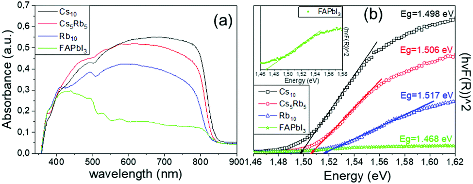 | ||
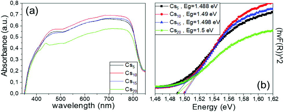
| Fig. 2 (a) UV-vis absorption spectra and (b) Tauc plots of the perovskite films under study (in the inset a focus in the FAPbI3 perovskite spectra is demonstrated for clarity). | ||
The absorption spectra obtained for the FAPbI3 perovskite distinctively demonstrate that there is no active perovskite phase formed, under particular fabrication conditions employed in this study. The absorbance is very low, even though the bandgap of the perovskite is confirmed to be at 1.47 eV. After the addition of Rb, there is a significant increase in the absorbance values, clearly indicating the increase in the light harvesting ability of the perovskite film. By introducing Cs and with increasing the amount, a further increase is noted in the absorbance values, which maximizes for the Cs10 perovskite, indicating the total replacement of Rb with Cs, suggesting that it will be the perovskite formulation to deliver the highest efficiency values in the corresponding solar cells. A simultaneous shift towards longer wavelengths is also recorded upon the partial or complete substitution of Rb with Cs, which in turn yields lower values of Eg, which are closer to the ideal bandgap for solar cell absorbers of 1.4 eV. Thus, we expect that the perovskite with the lowest Eg, which is in this case Cs10, will achieve devices with the highest photocurrent values.
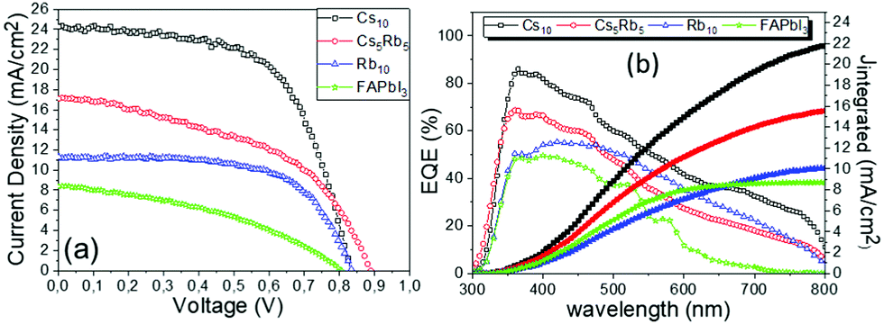 | ||
| Fig. 3 (a) Current density–voltage curves of the champion C-PSCs, incorporating the MA-free perovskites under study, under illumination of 100 mW cm−2 simulated sun irradiation (1.5 AM) and (b) EQE of the corresponding solar cells. | ||
| Perovskite | J sc (mA cm−2) | V oc (V) | FF | PCE (%) | J int. (mA cm−2) |
|---|---|---|---|---|---|
| FAPbI3 | 8.47 | 0.797 | 0.39 | 2.69 | 8.69 |
| Rb10 | 11.27 | 0.834 | 0.64 | 5.97 | 10.05 |
| Cs5Rb5 | 17.35 | 0.879 | 0.48 | 7.37 | 15.62 |
| Cs10 | 24.30 | 0.834 | 0.60 | 12.19 | 21.87 |
In the absence of any inorganic cations, that play the role of “stabilizing” the crystal structure of the formamidinium (FA) cation, in order for the perovskite active phase to be formed under low temperature conditions (<150 °C), the FAPbI3 perovskite yields a low performing device, when incorporated in ambient processed, HTL-free C electrode PSCs. In particular, the Voc value is acceptable, suggesting that the non-radiative recombination losses are not detrimental for the device performance. It is also an indication that the selection of transport layers is appropriate for the FA-based perovskites and that the infiltration of the precursor solution is successful.
However, the Jsc values obtained are distinctively low, justifying that the active phase of the perovskite is not formed, as also confirmed by the XRD measurements. Moreover, the low fill factor (FF) values obtained indicate that there are many charge transport losses occurring in this device, which are attributed to the reduced capability of FAPbI3 to effectively transport holes, in this HTL-free device configuration. By inserting a portion of the Rb cation in the perovskite precursor solution, a substantial increase in the device performance occurs. An increase in the Voc values by >35 mV, combined with an increase in the Jsc values by 33% and FF value of 0.64, which is very high for this particular type of device, leads to a more than two-fold increase in the PCE of the Rb10 perovskite-based device, that increases close to 6% vs. ∼2.7% for the plain FAPbI3 based C-PSC.
Even though this is a significant improvement, the performance of C-PSCs remains limited. Bearing in mind that the RbxFA1−xPbI3 perovskite films require a high annealing temperature (150 °C), as reported in the literature,29–31 something that has been purposely avoided in this study, in order to follow a construction protocol which will have the ability to be applied in large area devices, we can attribute this low performance to the inability of Rb10 to effectively be converted to the “black phase”.
With the addition of Cs, a further improvement of the C-PSC performance is achieved, with the PCE increasing up to 7.37%. This is mainly a consequence of the significant increase in the Jsc values, which increase up to 17.35 mA cm−2. This value is within acceptable limits, suggesting that the active perovskite phase is formed under the chosen fabrication conditions and highlighting the synergistic effects of Cs and Rb in promoting the lattice modification more effectively.29 An increase in the Voc values is also observed, while, in contrast, the FF presents a decrease after the addition of Cs.
By eliminating Rb and replacing it with an equimolar amount of Cs (Cs10), a significant increase is noted in the performance of the corresponding C-PSCs. A very high photocurrent value of 24.30 mA cm−2 is recorded together with a good Voc value of 834 mV and a FF reaching 0.6, which yields a final PCE as high as 12.19%, the highest that has been recorded in the frames of this study.
The superior performance and the capability of the Cs10 perovskite to deliver C-PSCs with enhanced photocurrent density values are also confirmed from the EQE spectra (Fig. 3b) that are obtained for the MA-free perovskites with different inorganic cations. The form of the spectra is that of a typical, HTL-free, C electrode PSC of the triple mesoscopic structure, where a decrease is noted beyond 600 nm.32–34
These results indicate the suitability of Cs, among the inorganic cations available, to effectively stabilize FA and achieve highly crystalline MA-free perovskite films that can be produced in low temperature and ambient conditions, which allows their application in HTL-free, C-PSCs with the potential of large area applications.
An additional feature that has been noted is the good reproducibility of the devices, as shown in Fig. 4. This is a feature of great importance, considering that the whole process of both the perovskite precursor solutions and the consequent C-PSC fabrication is conducted entirely under ambient conditions, with no control over humidity and oxygen and that we have chosen to use a low temperature annealing for the perovskites. Thus, we can conclude that the materials and methods proposed in this study are suitable for application on a large scale. The effect of the inorganic cation variation in the hysteresis of the MA-free carbon electrode based PSCs is evaluated by plotting the J–V curves in reverse and forward scanning modes (Fig. 5) and calculating the hysteresis index (HI) using the formula (Table 2):
 | (1) |
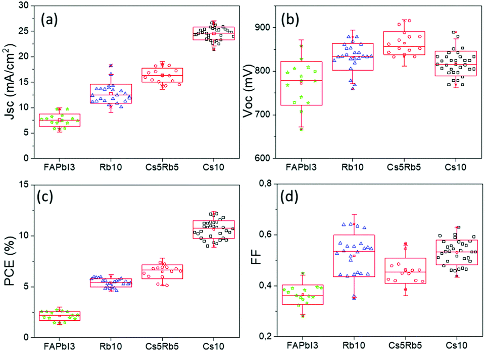 | ||
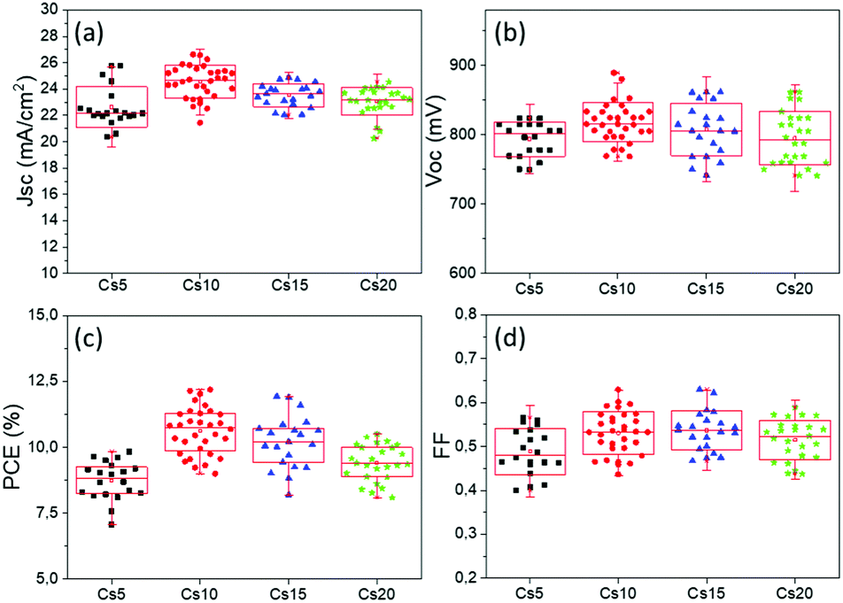
| Fig. 4 Statistical graphs illustrating the device performance statistics (20 devices for each condition) for C-PSCs incorporating the MA-free perovskites under study (a) Jsc, (b) Voc, (c) PCE, and (d) FF, represented in box-and-whisker plots. Device parameters are obtained from reverse J–V scans. | ||
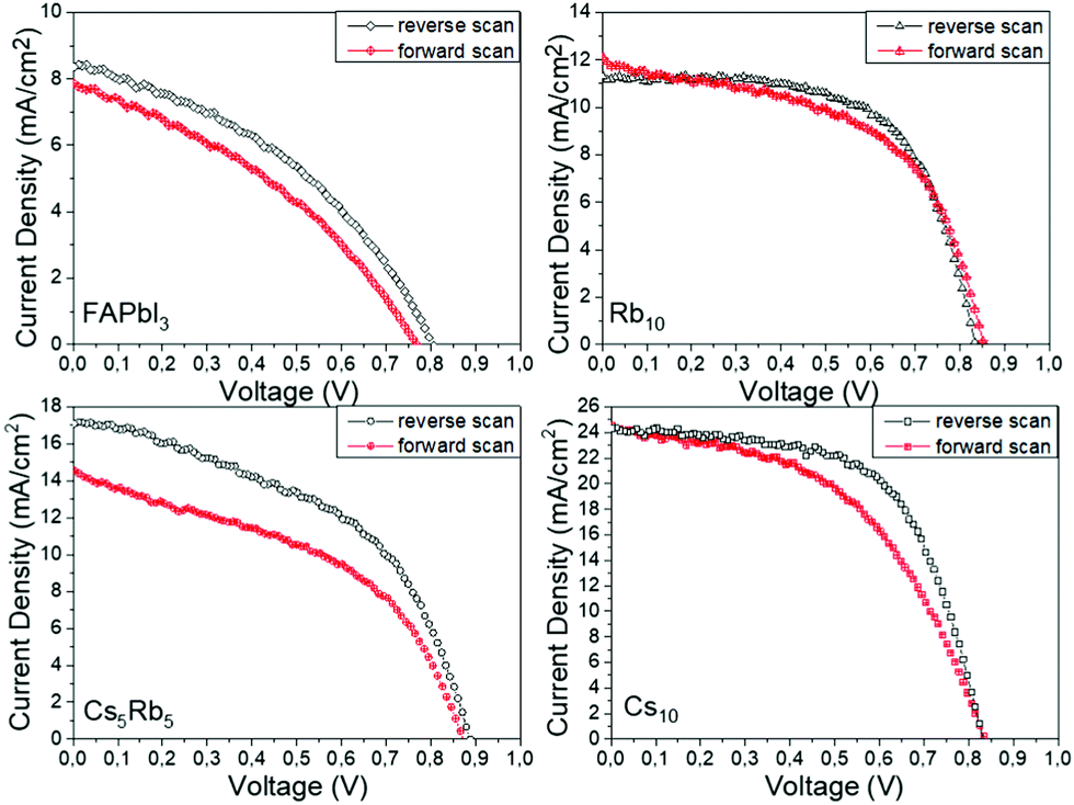 | ||
| Fig. 5 J–V curves of the highest performing C-PSCs prepared with the different perovskites under study, in forward and reverse scanning modes. | ||
| Perovskite | J sc (mA cm−2) | V oc (V) | FF | PCE (%) | HI |
|---|---|---|---|---|---|
| FAPbI3 | 7.87 | 0.777 | 0.35 | 2.16 | 0.20 |
| Rb10 | 12.09 | 0.861 | 0.53 | 5.49 | 0.08 |
| Cs5Rb5 | 14.55 | 0.876 | 0.41 | 5.19 | 0.29 |
| Cs10 | 24.54 | 0.843 | 0.49 | 10.09 | 0.17 |
The origin of the hysteresis in PSCs has been attributed to the unbalanced charge carrier transport, ion migration and trapping and detrapping of charge carriers.35,36 An interesting observation has been made for the case of Rb employed as the inorganic cation, where the R10 perovskite displayed the lowest HI of 0.08, even though the PCE of the devices remains low.
Combined with the very high FF values obtained, we can attribute this to the minimum defects in the perovskite film and the good perovskite film morphology. As it has been previously reported in the literature, Rb doping has proven to yield hysteresis-free PSCs31,36 and this observation is also confirmed for the particular PSC structure under study, where no HTL is employed and the Au counter electrode is replaced by a mesoscopic C electrode. The highest performing perovskite, Cs10, also exhibits devices with a HI of 0.17, which is low for this type of device configuration, that comprises 3 mesoporous layers while no HTL is employed.
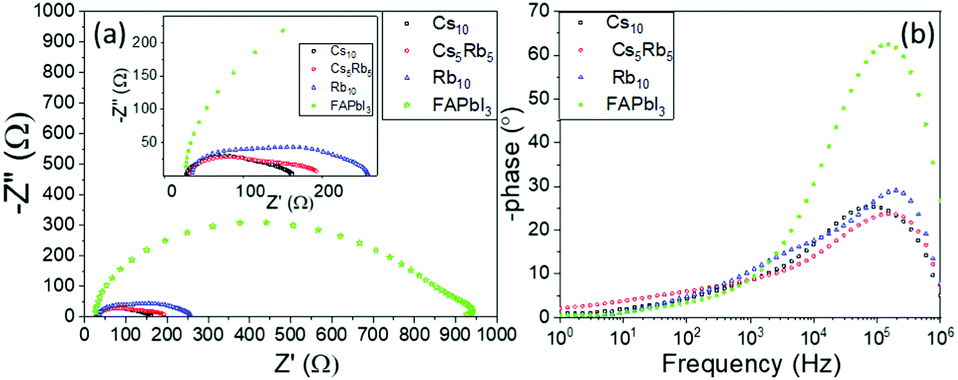 | ||
| Fig. 6 (a) Nyquist plots and (b) Bode phase plots obtained from electrochemical impedance spectroscopy (EIS) measurements, performed under illumination, at 0.8 V applied potential, on C-PSCs employing the different MA-free perovskites under study. A focus on the spectra obtained for the C-PSCs after the insertion of inorganic cations is demonstrated in the inset for clarity. | ||
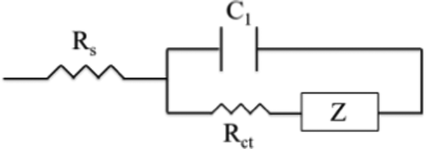 | ||
| Fig. 7 The Matryoshka (ladder-type) circuit that was used for the fitting of the experimental data obtained from the Nyquist plots after the application of EIS measurements. | ||
| Perovskite | Rs (Ohm) | R ct (Ohm) |
|---|---|---|
| FAPbI3 | 28.19 | 550 |
| Rb10 | 30.26 | 124 |
| Cs5Rb5 | 36.00 | 69.7 |
| Cs10 | 30.66 | 65.0 |
One profound semicircle appears in the high-frequency region (104–106 Hz) of the Nyquist plots of all perovskites under study; however, this element seems distorted for the C-PSCs implementing the Rb and Cs doped perovskites. This is also confirmed by the Bode phase plots, where a second small peak appears in the spectra, in the intermediate frequency region (10–104 Hz) and is mostly distinct in the Rb10 perovskite spectra.
This is related to the time constants of the different processes that take place, where the interfacial recombination observed mainly at intermediate frequencies and the charge transfer process observed at the high frequency region overlap, providing a “mixed” signal.
The high frequency region elements are attributed to the charge transfer process at the perovskite/C interface, considering that there is no contribution of the HTL in our devices.40,41 After the fitting of the experimental data, the values of the charge transfer resistance (Rct) are obtained (Table 3) and it becomes clear that the addition of both inorganic cations favors the extraction of the charge from the perovskite to the counter electrode, with a minimum value being recorded for the Cs10 perovskite, demonstrating that Cs allows for a better charge collection, which is an additional justification of this perovskite's formulation optimum performance.
The series resistance (Rs) element and dielectric contributions are depicted as the first point of the interception of the Nyquist spectra with the Z′ axis. Similar values are obtained after the fitting, demonstrating that the variation of inorganic cations has no significant effect in the series resistance of the C-PSCs. This is also an important observation, considering the fabrication process of the C-PSCs under study, where the perovskite is infiltrated through the 3 mesoporous layers (TiO2/ZrO2/C) and indicates that the inorganic cations do not alter the penetration capability of the perovskite precursor solution, that could be detrimental for the device performance.42
2. Cation structure investigation
The next step towards the exploration and optimization of MA-free perovskites for their application in C-PSCs of the triple mesoscopic structure is the optimization of inorganic component's content. More specifically, after having established Cs as the optimum inorganic cation, we proceeded to the evaluation of a series of inorganic/organic (Cs/FA) ratios on the perovskite film properties and their performance in HTL-free, C-PSCs prepared under ambient conditions and with low-temperature annealing. For simplicity reasons, the CsxFA1−xPbI3 perovskite formulations are denoted as Cs5 (5/95), Cs10 (10/90), Cs15 (15/85) and Cs20 (20/80), where the fractions in parentheses refer to the ratio of Cs/FA (x/1−x).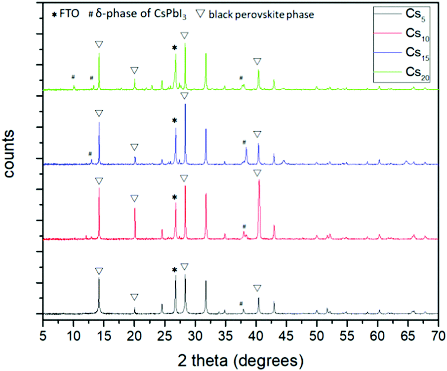 | ||
| Fig. 8 X-ray diffraction patterns of the C-PSCs prepared with the 4 perovskites under study. | ||
All of the spectra obtained present a distinctive peak at ∼26.7°, which is assigned to the FTO substrate.43–46 Considering that the intensity of this peak is the same in all measurements, we have used this peak as a reference to assure the validity of the obtained results (XRD peak origins and intensity). Even though we have used a low-temperature annealing to fabricate the perovskite films (100 °C), the peaks that correspond to the black perovskite phase of CsxFA1−xPbI3 appear in all the perovskite films under study. In particular, the most prominent peaks appear at 14.2°, 20.1°, 28.3° and 40.5°, which are assigned to the (101), (110), (202) and (220) planes, respectively. No shift of these peaks is observed with increasing amount of Cs, which indicates that the increase of the Cs amount has no effect on the crystal structure,47,48 bearing in mind that the shifts appearing in the XRD spectra of perovskites come as a result of changes in the crystal lattice parameters and of the crystal lattice strain.49–52
When we move from the lowest Cs/FA ratio of 5/95 (Cs5) to 10/90 (Cs10), a noticeable increase is observed for all the perovskite peak intensities, suggesting a better crystal quality, and predisposing for a higher C-PSC performance, by obtaining higher photocurrent values. With a further increase in the Cs content, the peaks of the δ-phase CsPbI3 start to appear at 10.2° and 38.4° and with a further increase to the 20/80 ratio (Cs20) at 13° additionally, which is undesirable for solar cell applications,53–55 while at the same time a significant reduction in the intensity of the (110) and (220) peaks suggests that the perovskite films have a lower crystal quality, together with a preferential oriented growth towards the (202) plane. The absence of the unreacted PbI2 peak at 12.7° is clear evidence of the complete transformation of the perovskite precursor to high quality perovskite films, which is of high importance considering that the whole fabrication process is conducted entirely under ambient conditions.
 | ||
| Fig. 9 (a) UV-vis absorption spectra and (b) Tauc plots of the Cs doped, MA-free perovskite films under study. | ||
The increase in the Cs content from 5% to 10% mol promotes an increase in the absorbance spectra over the whole visible range, which correlates well with the XRD measurements that revealed higher perovskite diffraction peaks for this Cs concentration. This is an additional indication of the optimum absorption ability of the perovskite film of this Cs/FA ratio and the corresponding C-PSCs incorporating this perovskite formulation are expected to yield high photocurrent values. Further increase in the Cs content results in diminishment of the absorbance values, which can be attributed to the initializing of the CsPbI3 inactive species formation, as also suggested by the XRD spectra obtained. On the other hand, the band-absorption edge for all Cs doped MA-free perovskite films prepared and studied remains unchanged, indicating the structural intactness of the perovskite lattice, in agreement with the absence of shifts in the XRD perovskite peaks. Therefore, we can conclude that the Cs content has no effect on the bandgap values of the resulting perovskite, while the optimum Cs/FA ratio, which provides the highest absorption, is 10/90.
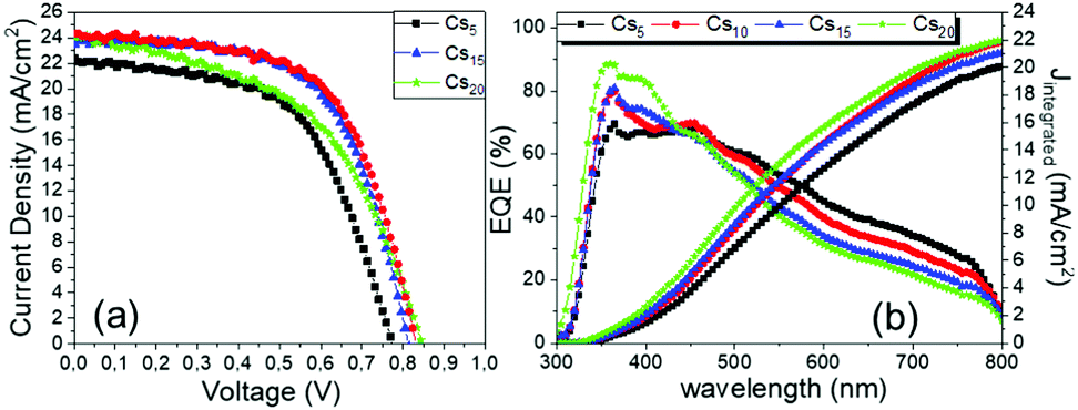 | ||
| Fig. 10 (a) Current density–voltage curves of the highest performing C-PSCs, incorporating the Cs doped, MA-free perovskites under study, under illumination of 100 mW cm−2 simulated sun irradiation (1.5 AM) and (b) EQE of the corresponding solar cells. | ||
| Perovskite | J sc (mA cm−2) | V oc (V) | FF | PCE (%) | J int. (mA cm−2) |
|---|---|---|---|---|---|
| Cs5 | 22.29 | 0.777 | 0.57 | 9.84 | 20.06 |
| Cs10 | 24.31 | 0.834 | 0.60 | 12.19 | 21.86 |
| Cs15 | 23.42 | 0.805 | 0.63 | 11.91 | 21.06 |
| Cs20 | 24.40 | 0.843 | 0.51 | 10.38 | 21.96 |
Starting from the lowest Cs content 5/95, the highest performing Cs doped MA-free perovskite (Cs5) based C-PSC exhibits a Jsc value of 22.29 mA cm−2, with a Voc of 777 mV, and a FF value of 0.57, which finally yields a PCE as high as 9.84%. This result is already promising enough, considering that the C-PSCs are HTL-free and prepared entirely under ambient conditions, using low cost methods and low temperature perovskite annealing.
With the increase of Cs and a simultaneous reduction of the FA content, a systematic increase in the photocurrent values is observed, in line with the results obtained from both the XRD and absorbance measurements, confirming that a Cs content higher than 5% improves the crystallinity of the perovskite films, leading to optimum light absorption ability and consequently delivering high photocurrent values in the corresponding devices. These results are also confirmed by the statistical graphs of the Jscvs. Cs content (Fig. 11a), where it is observed that the mean value of Jsc is systematically higher for the Cs content over 10% mol, compared to the values obtained for Cs 5% mol, while the highest mean value is recorded for the 10/90 Cs/FA molar ratio (Cs10). The trend in the Jsc values as well as the effect of the Cs content on the performance of the C-PSCs is also elucidated from the EQE spectra obtained (Fig. 10b).
 | ||
| Fig. 11 Statistical graphs illustrating the device performance statistics (>20 devices for each condition) for C-PSCs incorporating the MA-free perovskites under study (a) Jsc, (b) Voc, (c) FF, and (d) PCE, represented in box-and-whisker plots. Device parameters are obtained from reverse J–V scans. | ||
The Voc values do not follow the same trend; as it can be seen in the statistical graphs of the Voc values with the varying Cs content (Fig. 11b), the mean value of Voc remains almost constant, presenting a small increase only for the 10/90 Cs doped perovskite. A slight enhancement in the FF values is also observed, the highest ones being recorded for 10/90 and 15/85 perovskites (Cs10 and Cs15, respectively).
Overall, the perovskites with the Cs content equal to or higher than 10% mol exhibit higher PCEs compared to the perovskite with 5% mol Cs, owing mainly to the enhanced Jsc valued recorded. More specifically, the 10/90 perovskite composition delivers a Jsc value of 24.31 mA cm−2, combined with a Voc value of 0.834 V and a FF of 0.6, which results in the highest PCE obtained in this study of 12.19%. Even though the PCE of the 15/85 perovskite, which is 11.91%, is very close to the one obtained for 10/90, we can see from the statistical graphs of the PCE vs the Cs content (Fig. 11c) that the mean value of the 10/90 perovskite is also higher than the one obtained for 15/85; hence we can conclude that the optimum Cs/FA ratio is 10/90 for the MA-free perovskites applied in HTL-free, C-PSCs of the triple mesoscopic structure.
The hysteresis index (HI) for the highest performing C-PSCs of each Cs/FA ratio is also calculated, after plotting the J–V curves in reverse and forward scanning modes (Fig. 12), by using the formula presented as eqn (1) in a previous page. The results are summarized in Table 5 and elucidated the effect of the Cs content on the hysteresis of the devices. The lowest HI value is recorded for the 10/90 perovskite, which combined with the highest PCE values (maximum and mean) that this perovskite formulation exhibits confirms that the optimum Cs/FA ratio has been reached.
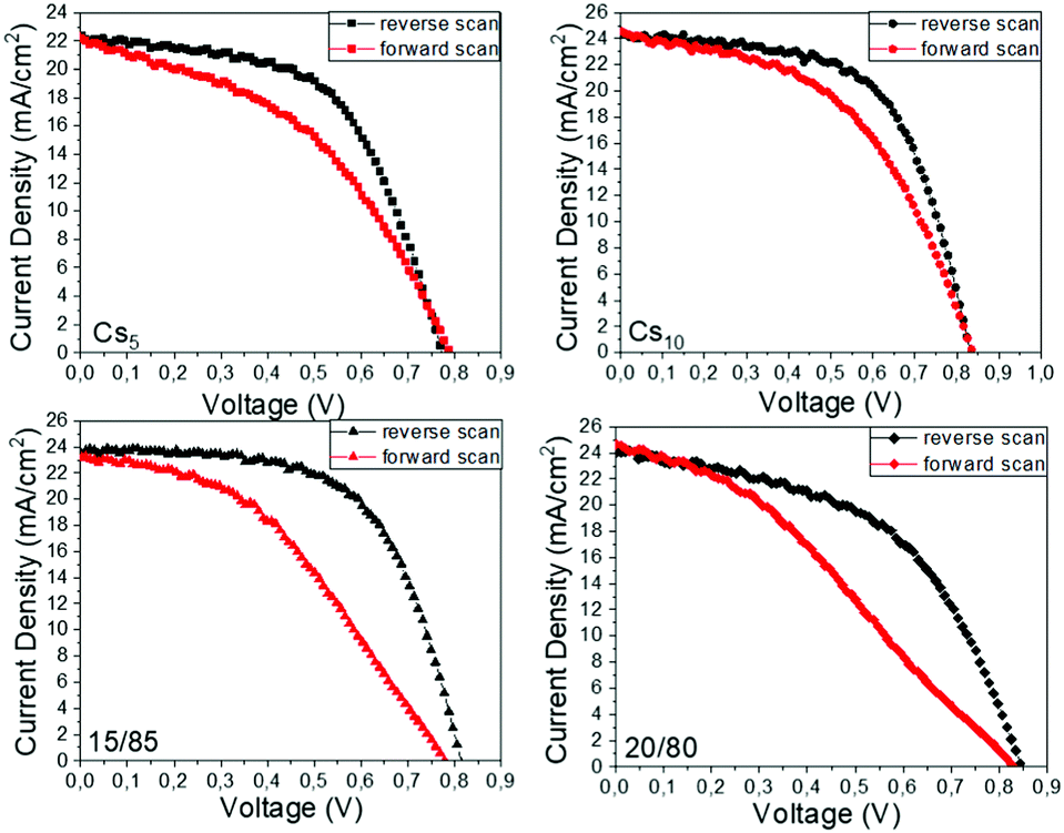 | ||
| Fig. 12 J–V curves of the highest performing C-PSCs prepared with the Cs doped, MA-free perovskites under study, in forward and reverse scanning modes. | ||
| Perovskite | J sc (mA cm−2) | V oc (V) | FF | PCE (%) | HI |
|---|---|---|---|---|---|
| Cs5 | 22.17 | 0.796 | 0.44 | 7.68 | 0.22 |
| Cs10 | 24.54 | 0.843 | 0.49 | 10.09 | 0.17 |
| Cs15 | 23.20 | 0.788 | 0.41 | 7.56 | 0.37 |
| Cs20 | 24.64 | 0.824 | 0.33 | 6.81 | 0.34 |
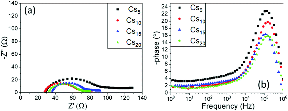 | ||
| Fig. 13 (a) Nyquist plots and (b) Bode phase plots obtained from electrochemical impedance spectroscopy (EIS) measurements, performed under illumination, at 0.8 V applied potential, on C-PSCs employing the Cs doped, MA-free perovskites under study. | ||
| Perovskite | R s (Ohm) | R ct (Ohm) |
|---|---|---|
| Cs5 | 30.89 | 47.8 |
| Cs10 | 29.80 | 31.4 |
| Cs15 | 37.26 | 29.7 |
| Cs20 | 32.25 | 34.2 |
One prominent semicircle is present in the Nyquist plot for all the Cs doped MA-free perovskites under study, obtained in the high frequency region as also confirmed from the Bode phase plots, and is attributed to the charge transfer process between the perovskite and the C electrode. With increasing Cs content, a diminishment is recorded in the Rct values, which correlates well with the increase in the generated photocurrent of these devices. The series resistance values do not demonstrate significant changes, like in the variation of the inorganic cation type, which has been an expected outcome in this case, since the composition of the perovskite precursor solution is subjected to a minimum change, which could not affect the physical and chemical parameters that determine its affinity with the mesoporous layers of the device architecture.
Conclusions
In this study we proceeded to the optimization of the composition of MA-free, FA-based perovskites for application in carbon electrode based, hole transport layer (HTL) free perovskite solar cells (PSCs). Both the perovskite precursor solutions and the device preparation have been conducted entirely under ambient conditions, while the annealing of the perovskites has been performed under low temperature conditions (100 °C), in order to reduce the energy cost and qualify for large area applications. Firstly, the effect of the inorganic salt type, used as a stabilizing cation to the pure FAPbI3 perovskite has been investigated, which has highlighted the potential of Cs, among Rb+, Cs+ and a combination of both. The incorporation of Cs+, through CsI addition in the perovskite precursor solution, has led to optimum crystallization, as revealed by XRD measurements and optimum absorption ability, as confirmed by UV-vis measurements, leading to a champion PCE of ∼12.2% for the corresponding C-PSCs. An additional optimization of the Cs content in the CsxFA1−xPbI3 perovskite has revealed that the optimum ratio of Cs/FA for high performing devices is 10/90. This ratio provides the highest PCE, along with the lowest series resistance (Rs) and a low charge transfer resistance (Rct), as elucidated from electrochemical impedance spectroscopy that was performed in a series of CsxFA1−xPbI3 C-PSCs, with a varying Cs/FA ratio. All the devices under study, regardless of their composition and performance, present low hysteresis index (HI) values and a good reproducibility, which highlights the suitability of the proposed fabrication method for the preparation of efficient MA-free, HTL-free, carbon electrode PSCs, under low cost, low temperature, ambient conditions, opening the way for implementation in a variety of solar cell devices, including PSC modules, flexible devices and tandem applications. The results of this work, combined with the well-known increased stability of MA-free perovskites, have provided the motivation for a further stability study of ambient processed, HTL-free, C electrode based PSCs, which is currently in progress and will be the next step of this study, providing a thorough investigation of this particular PSC design. Moreover, this work paves the way towards alternative applications of C-PSCs of the triple mesoscopic structure, such as their incorporation in low light intensity conditions, such as indoor photovoltaics, where C-PSCs prevail over the traditional PSCs, owing to their low cost, combined with PCEs that exceed 11% and high stability, with minor degradation occurring at illuminance values <1000 lux.56 Combined with the elimination of antisolvent during the fabrication process and the high reproducibility of the results, the expansion of this work and incorporation in large area devices are expected to be highly promising with a great potential for market uptake.Experimental
Chemicals and materials
Unless otherwise specified, all the reagents were purchased from Sigma-Aldrich and were used as received. Formamidinium iodide (FAI) was purchased from Dyenamo. Commercial nanocrystalline Titania paste 18-NRT was purchased from Greatcell and SnO2:F transparent conductive electrodes (FTO, Resistance 10 Ohm square−1) were purchased from Pilkington.Preparation of the ZrO2 paste
For the preparation of the ZrO2 paste, 1 g of ZrO2 (nanopowder <100 nm), 0.3 g of TiO2 (Degussa P25) and 1.4 g of ethyl cellulose powder were mixed and ground in a mortar. Then 0.5 mL of acetic acid was added, followed by the addition of 2 mL of distilled water under continuous grinding. 12 mL of absolute ethanol was then gradually added to the slurry, followed by 4.8 g of terpineol. Finally, the mixture was stirred for 5 min followed by 1 min sonication and additional stirring for 5 min.Preparation of the C paste
9 g of graphite powder (particle size <20 μm), 3 g of carbon black (Cabot Corporation) and 1 g of ZrO2 (nanopowder <100 nm) were mixed in a mortar. Then 18 g of terpineol was gradually added to the mixture while grinding. Finally, 15 g of ethyl cellulose solution (10 wt%) in absolute ethanol was gradually added. This process ends by 1 min sonication followed by 5 min of magnetic stirring. The addition of ZrO2 is necessary to facilitate the adhesion of C onto the underlying ZrO2 layer and improve the interface between these two materials.Perovskite precursor solution synthesis
All the perovskite precursor solutions were prepared under ambient conditions, inside a fume hood. For the preparation of the FAPbI3 perovskite, PbI2 (1.2 M) and FAI (1 M) were inserted in a mixture of DMF![[thin space (1/6-em)]](https://www.rsc.org/images/entities/char_2009.gif) :DMSO (4:1 v/v) and stirred at 70 °C for 1 h. For the preparation of CsxRbyFA1−x−yPbI3 perovskites, the appropriate amounts of cesium iodide (CsI) and rubidium iodide (RbI) were inserted, to reach the desired molar ratio (with respect to PbI2). For simplicity reasons, the below code names are used throughout the manuscript:
:DMSO (4:1 v/v) and stirred at 70 °C for 1 h. For the preparation of CsxRbyFA1−x−yPbI3 perovskites, the appropriate amounts of cesium iodide (CsI) and rubidium iodide (RbI) were inserted, to reach the desired molar ratio (with respect to PbI2). For simplicity reasons, the below code names are used throughout the manuscript:
• Rb0.1FA0.9PbI3 = Rb10
• Cs0.05Rb0.05FA0.9PbI3 = Cs5Rb5
• Cs0.05FA0.95PbI3 = Cs5
• Cs0.1FA0.9PbI3 = Cs10
• Cs0.15FA0.85PbI3 = Cs15
• Cs0.2FA0.8PbI3 = Cs20
Device fabrication
The device architecture of all the devices under study is the triple mesoscopic structure of the FTO/c-TiO2/mp-TiO2/ZrO2/C type, where the different perovskite precursor solutions have been infiltrated through the mesoporous stack and then spin-coated to obtain a homogeneous film. In particular, fluorine doped tin oxide (FTO, 10 Ohm square−1) glass substrates were chemically etched by reacting Zn powder with 4 M HCl, to form the desired pattern. The etched substrates were subsequently immersed in a surfactant solution (Triton-X 10 wt% in distilled water), deionized water, acetone and isopropanol and placed in an ultrasonic bath for 15 min per cleaning step. After the last rinse with isopropanol, the clean substrates were annealed at 500 °C, in order to remove any organic residuals. The compact TiO2 layer (c-TiO2) was deposited by spin coating 40 μL of Ti-diisopropoxide bis(acetyl)acetonate (75% in isopropanol, diluted by 1:9 v/v in N-propanol) at 2000 rpm for 10 s. The spin-coated films were dried at 125 °C and then annealed at 500 °C for 10 minutes and the procedure was repeated 4 times. The mesoporous TiO2 layer (m-TiO2) was then deposited by spin coating 40 μL of the TiO2 paste (18-NRT, diluted in ethanol 1:6 w/v) at 4000 rpm for 20 s, followed by drying at 125 °C and annealing at 525 °C for 30 minutes. The mesoporous films were post-treated with aqueous TiCl4 solution (40 mM), using the chemical bath deposition method conducted at 70 °C for 1 h, which was followed by annealing at 450 °C for 1 h. After cooling down, ZrO2 was deposited on the substrates, by doctor blading a quantity of the as prepared paste, followed by spin coating at 5000 rpm for 30 s, in order to obtain a homogeneous film with full coverage. The films were then annealed at 450 °C for 20 minutes. Finally, the C counter electrodes, with a thickness of ∼20 μm, as defined by the spacer that was used, were deposited by doctor blading a quantity of the as prepared paste, followed by annealing at 400 °C for 30 minutes. The perovskite solution, kept at 70 °C, was infiltrated through the C electrode for 30 s, followed by spin coating at 1000 rpm for 10 s and 5000 rpm for 20 s. The perovskite loaded substrates were then placed for annealing at 100 °C, for 60 min, capped by a Petri dish. After annealing, the perovskite films were washed with isopropanol, by dropping 80 μL of the solvent and spin coating at 6000 rpm for 10 s. No hole transport material and no antisolvent dripping were used, while the whole process was performed entirely under ambient conditions (RT 25 °C and RH 25–30%). The thickness of each layer was optimized according to a previous report.57
Characterization
The crystallinity of the perovskite films was examined by X-ray diffraction (XRD) measurements using a Bruker D8 Advance diffractometer with CuKα radiation (λ = 1.5418 Å) in a 2θ range of 2° to 80° at a scanning rate of 2° min−1. The measurement was performed in complete devices, in order to obtain realistic and reliable data about the capability of the perovskites to crystallize within the pores of the triple mesoscopic substrate, and particularly the mesoporous C layer, which is the most prominent challenge regarding the carbon electrode perovskite solar cells so far.The ultraviolet-visible/NIR absorption diffuse reflectance spectra of the perovskite films were obtained in the range of 300 nm to 850 nm using a Jasco V-770 spectrophotometer equipped with a 60 mm integrating sphere embedding a PbS Detector (ISN-923).
Photocurrent density–voltage (J–V) curves were recorded using a Keithley 2601 source meter, with an applied potential range from 1.1 to −0.1 V and a scan rate of 125 mV s−1, by illumination using a Solar Light simulator providing a beam of 100 mW cm−2 light intensity. In order to determine the active area of the devices, a black metallic mask of aperture size 0.145 cm2, which is close to the actual area of the devices, as proposed by Kamat et al.58 was used. External quantum efficiency (EQE) was determined using an incident photo to current efficiency measurement apparatus (Thetametrisis PM-QE) equipped with a xenon (Xe) light source using a filter monochromator (Oriel CornerstoneTM 260 1/4 m, Newport) which was controlled by the PM-Monitor® software. Electrochemical impedance spectroscopy (EIS) characterization was performed on PSC devices with a potentiostat/galvanostat (PGSTAT128 N, Autolab B.V., Netherlands) under AM-1.5G illuminated conditions.
Conflicts of interest
There are no conflicts to declare.Acknowledgements
This work was co-funded by the European Union and the General Secretariat of Research and Technology, Ministry of Education, Research Religious Affairs under the project “PrintPero” of the Bilateral R&T Cooperation Program Greece-Germany 2018–2021 (project code: T2ΔΓE-0560, MIS: 5030132).References
- https://www.nrel.gov/pv/cell-efficiency.html .
- J. Li, Q. Dong, N. Li and L. Wang, Adv. Energy Mater., 2017, 7, 1602922 CrossRef.
- B. Rivkin, P. Fassl, Q. Sun, A. D. Taylor, Z. Chen and Y. Vaynzof, ACS Omega, 2018, 3, 10042–10047 CrossRef CAS PubMed.
- S. Guo, X. Sun, C. Ding, R. Huang, M. Tan, L. Zhang, Q. Luo, F. Li, J. Jin and C.-Q. Ma, Energy Technol., 2020, 8, 2000250 CrossRef CAS.
- A. Guerrero, J. You, C. Aranda, Y. S. Kang, G. Garcia-Belmonte, H. Zhou, J. Bisquert and Y. Yang, ACS Nano, 2016, 10, 218–224 CrossRef CAS PubMed.
- Z. Ku, Y. Rong, M. Xu, T. Liu and H. Han, Sci. Rep., 2013, 3, 3132 CrossRef PubMed.
- S. Liu, W. Huang, P. Liao, N. Pootrakulchote, H. Li, J. Lu, J. Li, F. Huang, X. Shai, X. Zhao, Y. Shen, Y.-B. Cheng and M. Wang, J. Mater. Chem. A, 2017, 5, 22952–22958 RSC.
- J. H. Noh, S. H. Im, J. H. Heo, T. N. Mandal and S. Il Seok, Nano Lett., 2013, 13, 1764–1769 CrossRef CAS PubMed.
- S. Rühle, Sol. Energy, 2016, 130, 139–147 CrossRef.
- B. Conings, J. Drijkoningen, N. Gauquelin, A. Babayigit, J. D’Haen, L. D’Olieslaeger, A. Ethirajan, J. Verbeeck, J. Manca, E. Mosconi, F. De Angelis and H.-G. Boyen, Adv. Energy Mater., 2015, 5, 1500477 CrossRef.
- R. K. Misra, S. Aharon, B. Li, D. Mogilyansky, I. Visoly-Fisher, L. Etgar and E. A. Katz, J. Phys. Chem. Lett., 2015, 6, 326–330 CrossRef CAS PubMed.
- Y. Han, S. Meyer, Y. Dkhissi, K. Weber, J. M. Pringle, U. Bach, L. Spiccia and Y.-B. Cheng, J. Mater. Chem. A, 2015, 3, 8139–8147 RSC.
- N. Pellet, P. Gao, G. Gregori, T.-Y. Yang, M. K. Nazeeruddin, J. Maier and M. Grätzel, Angew. Chem., Int. Ed., 2014, 53, 3151–3157 CrossRef CAS PubMed.
- G. E. Eperon, S. D. Stranks, C. Menelaou, M. B. Johnston, L. M. Herz and H. J. Snaith, Energy Environ. Sci., 2014, 7, 982–988 RSC.
- J.-W. Lee, D.-J. Seol, A.-N. Cho and N.-G. Park, Adv. Mater., 2014, 26, 4991–4998 CrossRef CAS PubMed.
- T. M. Koh, K. Fu, Y. Fang, S. Chen, T. C. Sum, N. Mathews, S. G. Mhaisalkar, P. P. Boix and T. Baikie, J. Phys. Chem. C, 2014, 118, 16458–16462 CrossRef CAS.
- M. T. Weller, O. J. Weber, J. M. Frost and A. Walsh, J. Phys. Chem. Lett., 2015, 6(16), 3209–3212 CrossRef CAS.
- L.-Q. Xie, L. Chen, Z.-A. Nan, H.-X. Lin, T. Wang, D.-P. Zhan, J.-W. Yan, B.-W. Mao and Z.-Q. Tian, J. Am. Chem. Soc., 2017, 139(9), 3320–3323 CrossRef CAS PubMed.
- W. Rehman, D. P. McMeekin, J. B. Patel, R. L. Milot, M. B. Johnston, H. J. Snaith and L. M. Herz, Energy Environ. Sci., 2017, 10, 361–369 RSC.
- M. Saliba, T. Matsui, J.-Y. Seo, K. Domanski, J.-P. Correa-Baena, M. K. Nazeeruddin, S. M. Zakeeruddin, W. Tress, A. Abate, A. Hagfeldt and M. Grätzel, Energy Environ. Sci., 2016, 9, 1989–1997 RSC.
- A. Amat, E. Mosconi, E. Ronca, C. Quarti, P. Umari, M. K. Nazeeruddin, M. Grätzel and F. De Angelis, Nano Lett., 2014, 14, 3608–3616 CrossRef CAS PubMed.
- Z. Li, M. Yang, J.-S. Park, S.-H. Wei, J. J. Berry and K. Zhu, Chem. Mater., 2016, 28, 284–292 CrossRef CAS.
- V. M. Goldschmidt, Naturwissenschaften, 1926, 14, 477–485 CrossRef CAS.
- S. Phadke, R. Mysyk and M. Anouti, J. Energy Chem., 2020, 40, 31–38 CrossRef.
- Y. Hu, E. M. Hutter, P. Rieder, I. Grill, J. Hanisch, M. F. Aygüler, A. G. Hufnagel, M. Handloser, T. Bein, A. Hartschuh, K. Tvingstedt, V. Dyakonov, A. Baumann, T. J. Savenije, M. L. Petrus and P. Docampo, Adv. Energy Mater., 2018, 8, 1703057 CrossRef.
- Y. Hu, M. F. Aygüler, M. L. Petrus, T. Bein and P. Docampo, ACS Energy Lett., 2017, 2, 2212–2218 CrossRef CAS.
- J. Tauc, Mater. Res. Bull., 1968, 3, 37–46 CrossRef CAS.
- J. Tauc, Amorphous and Liquid Semiconductors, Springer, Boston, MA, 1974, p. 159 Search PubMed.
- S. H. Turren-Cruz, A. Hagfeldt and M. Saliba, Science, 2018, 362, 449–453 CrossRef CAS PubMed.
- Y. H. Park, I. Jeong, S. Bae, H. J. Son, P. Lee, J. Lee, C. H. Lee and M. J. Ko, Adv. Funct. Mater., 2017, 27, 21–27 Search PubMed.
- M. Saliba, T. Matsui, K. Domanski, J.-Y. Seo, A. Umnadisingu, S.-M. Zakeeruddin, J.-B. Correa-Baena, W.-R. Tress, A. Abate, A. Hagfeldt and M. Grätzel, Science, 2016, 354, 206–209 CrossRef CAS PubMed.
- T. Liu, L. Liu, M. Hu, Y. Yang, L. Zhang, A. Mei and H. Han, J. Power Sources, 2015, 293, 533–538 CrossRef CAS.
- X. Hou, Y. Hu, H. Liu, A. Mei, X. Li, M. Duan, G. Zhang, Y. Rong and H. Han, J. Mater. Chem. A, 2017, 5, 73–78 RSC.
- J. Chen, Y. Xiong, Y. Rong, A. Mei, Y. Sheng, P. Jiang, Y. Hu, X. Li and H. Han, Nano Energy, 2016, 27, 130–137 CrossRef CAS.
- H. J. Snaith, A. Abate, J. M. Ball, G. E. Eperon, T. Leijtens, N. K. Noel, S. D. Stranks, J. T.-W. Wang, K. Wojciechowski and W. Zhang, J. Phys. Chem. Lett., 2014, 5, 1511–1515 CrossRef CAS PubMed.
- R. Singh and M. Parashar, Soft-Matter Thin Film Solar Cells, AIP Publishing, 2021, pp. 1–42 Search PubMed.
- A. Todinova, L. Contreras-Bernal, M. Salado, S. Ahmad, N. Morillo, J. Idígoras and J. A. Anta, ChemElectroChem, 2017, 4, 2891–2901 CrossRef CAS.
- A. Guerrero, G. Garcia-Belmonte, I. Mora-Sero, J. Bisquert, Y. S. Kang, T. J. Jacobsson, J. P. Correa-Baena and A. Hagfeldt, J. Phys. Chem. C, 2016, 120, 8023–8032 CrossRef CAS.
- A. Bou, A. Pockett, D. Raptis, T. Watson, M. J. Carnie and J. Bisquert, J. Phys. Chem. Lett., 2020, 11, 8654–8659 CrossRef CAS PubMed.
- S. M. Abdulrahim, Z. Ahmad, J. Bahadra and N. J. Al-Thani, Nanomater, 2020, 10 Search PubMed.
- M. Wang, W.-L. Yim, P. Liao and Y. Shen, ChemistrySelect, 2017, 2, 4469–4477 CrossRef CAS.
- M. Bidikoudi, C. Simal, V. Dracopoulos and E. Stathatos, Mol., 2021, 26 Search PubMed.
- M. Jawad, A. F. Khan, A. Waseem, A. H. Kamboh, M. Mohsin, S. A. Shahzad, S. H. Shah, S. Mathur and A. J. Shaikh, Appl. Nanosci., 2020, 10, 485–497 CrossRef CAS.
- K. Ravichandran, R. Anandhi, K. Karthika, P. V. Rajkumar, N. Dineshbabu and C. Ravidhas, Superlattices Microstruct., 2015, 83, 121–130 CrossRef CAS.
- W. H. Kim, S. Woo, K. P. Kim, S. M. Kwon and D. H. Kim, Nanoscale Res. Lett., 2019, 14, 0–8 Search PubMed.
- W.-Y. Chen, L.-L. Deng, S.-M. Dai, X. Wang, C.-B. Tian, X.-X. Zhan, S.-Y. Xie, R.-B. Huang and L.-S. Zheng, J. Mater. Chem. A, 2015, 3, 19353–19359 RSC.
- M. Rameez, E. Y.-R. Lin, P. Raghunath, S. Narra, D. Song, M.-C. Lin, C.-H. Hung and E. W.-G. Diau, ACS Appl. Mater. Interfaces, 2020, 12, 21739–21747 CrossRef CAS PubMed.
- H. Li, X. Jiang, Q. Wei, Z. Zang, M. Ma, F. Wang, W. Zhou and Z. Ning, Angew. Chem., Int. Ed., 2021, 60, 16330–16336 CrossRef CAS PubMed.
- S. Kavadiya, J. Strzalka, D. M. Niedzwiedzki and P. Biswas, J. Mater. Chem. A, 2019, 7, 12790–12799 RSC.
- S. Dharani, H. A. Dewi, R. R. Prabhakar, T. Baikie, C. Shi, D. Yonghua, N. Mathews, P. P. Boix and S. G. Mhaisalkar, Nanoscale, 2014, 6, 13854–13860 RSC.
- A. J. Knight, J. Borchert, R. D. J. Oliver, J. B. Patel, P. G. Radaelli, H. J. Snaith, M. B. Johnston and L. M. Herz, ACS Energy Lett., 2021, 6, 799–808 CrossRef CAS PubMed.
- J. Zhao, Y. Deng, H. Wei, X. Zheng, Z. Yu, Y. Shao, J.-E. Shield and J. Huang, Sci. Adv., 2017, 3, eaao5616 CrossRef PubMed.
- X. Xu, C. Ma, Y.-M. Xie, Y. Cheng, Y. Tian, M. Li, Y. Ma, C.-S. Lee and S.-W. Tsang, J. Mater. Chem. A, 2018, 6, 7731–7740 RSC.
- Q. Wang, X. Zheng, Y. Deng, J. Zhao, Z. Chen and J. Huang, Joule, 2017, 1, 371–382 CrossRef CAS.
- Q. Ye, Y. Zhao, S. Mu, P. Gao, X. Zhang and J. You, Sci. China: Chem., 2019, 62, 810–821 CrossRef CAS.
- C. Polyzoidis, K. Rogdakis and E. Kymakis, Adv. Energy Mater., 2021, 11, 2101854 CrossRef CAS.
- M. Bidikoudi, C. Simal and E. Stathatos, ACS Appl. Energy Mater., 2021, 4(9), 8810–8823 CrossRef CAS.
- J. A. Christians, J. S. Manser and P. V. Kamat, J. Phys. Chem. Lett., 2015, 6, 852–857 CrossRef CAS PubMed.
Footnote |
| † Electronic supplementary information (ESI) available. See DOI: 10.1039/d1ya00037c |
| This journal is © The Royal Society of Chemistry 2022 |