
Molecular mechanics of Ag nanowire transfer processes subjected to contact loading by a PDMS substrate†
Minseok
Kang
ab,
Hyunkoo
Lee
 ab,
Sukjoon
Hong
*ab and
Joonmyung
Choi
*ab
ab,
Sukjoon
Hong
*ab and
Joonmyung
Choi
*ab
aDepartment of Mechanical Design Engineering, Hanyang University, 222 Wangsimni-ro Seongdong-gu, Seoul, 04763, Republic of Korea. E-mail: sukjoonhong@hanyang.ac.kr; joonchoi@hanyang.ac.kr
bDepartment of Mechanical Engineering, BK21 FOUR ERICA-ACE Center, Hanyang University, 55 Hanyangdaehak-ro, Sangnok-gu, Ansan, 15588, Republic of Korea
First published on 24th June 2022
Abstract
Precise transfer and attachment of a single nanowire to a target substrate is an interesting technique in surface engineering. The spacing, which restrains the attachment of a nanowire to a substrate, and the bending strain that occurs when the nanowire detaches from the elastomeric donor are important design parameters. In this regard, in this study, all-atom molecular dynamics (MD) simulations were conducted to analyse the mechanical behaviour of a penta-twinned silver nanowire (AgNW) placed on a polydimethylsiloxane (PDMS) donor substrate to elucidate the relevant transfer process. The bow deformation of the AgNW at the delamination front of PDMS was characterized as a function of its diameter and aspect ratio. The mechanisms of dislocation slip and propagation as well as the internal stress distribution of the AgNW were then examined. The results showed that twin boundary formation during the bow deformation is a key factor affecting the strain hardening of the AgNW and leading to complete plastic strain recovery after the removal of the PDMS substrate. Furthermore, the process was demonstrated experimentally by a localized bonding and transfer of AgNWs by continuous-wave laser irradiation. Based on the computational and experimental findings, an empirical model considering the shape parameters of AgNWs that can ensure a successful transfer process was established, which is essential for high-performance AgNW electrode design.
New conceptsThe laser-induced transfer process of a single silver nanowire (AgNW) and its sub-continuum mechanics have been characterized under stringent conditions. This is the first study to comprehend the bow deformation experienced when an AgNW is separated from the donor substrate during the transfer process. According to the diameter and aspect ratio of AgNWs, the non-covalent bonding force with the donor substrate and the subsequent mechanical damage were analysed. When the diameter and aspect ratio of the AgNW reached certain values, a large stress release occurred along with V-shape defects at the center, instead of breakage at the edge in the middle of the bow deformation process. The defects were almost eliminated after the separation of the donor substrate, and the AgNW returned to its pristine state by strain recovery. This suggests the possibility of the recovery of the AgNW to an intact state, providing promising results for the design of nanoelectromechanical systems using single nanowires. Such nanogeometric effects were also experimentally demonstrated through the technique of site-selective bonding by laser irradiation. In terms of the experimental technology, the present study is the first to successfully transfer a single AgNW to an acceptor by site-selective laser irradiation on both ends. |
Introduction
Metallic one-dimensional nanoscale structures, nanowires, have generated significant interest over the past three decades. Among them, silver nanowires (AgNWs) are one of the most promising nanostructures. This is owing to their excellent electrical conductivity (5285 S cm−1),1 higher modulus of elasticity (73–176 GPa) compared to bulk silver,2 low sheet resistance (13 Ω sq−1),3 and high transmittance (∼85%) over the entire visible wavelength range4 as a percolation network. AgNWs can be synthesized in high yields using the polyol method,5 and their diameter and length can be effectively adjusted by the solvothermal method.6 AgNWs can be used as flexible transparent electrodes,7–12 and recently, research has been conducted on applications such as biosensing devices, nanogenerators, touch screens, and solar cells.13–20 It is also particularly important to comprehend the internal crystal structures of AgNWs in terms of their conductivity characteristics. Therefore, the measurement of atomic levels of internal structures has been conducted in depth using field emission scanning electron microscopy (FESEM) and high-resolution transmission electron microscopy (HRTEM).21,22 Based on these analyses, the dislocation structures and defect distributions of AgNWs have been characterized and their correlations with the structural properties have been elucidated.23This unique property of AgNWs mainly originates from their geometry, including diameter (D), aspect ratio (AR), and crystallographic orientation. Typically, AgNWs grow radially along the [110] direction, and their cross-section has a pentagonal shape with five-fold twin boundaries (TBs). Understanding the atomic-scale structures of AgNWs is particularly important for characterizing mechanical behaviours such as strain hardening. Moreover, nucleation of dislocations on slip planes in response to a mechanical deformation determines the maximum strength of the overall nanostructure.24 Concurrently, the D and AR are decisive factors that determine the mechanical properties from a structural perspective, influencing the buckling load, strain-to-failure, and threshold radius of curvature.25 Accordingly, it is important to understand the relationship between the atomic structure and apparent geometry of a nanowire under a mechanical load.
Numerous studies have been conducted to characterize the mechanical behaviours and properties of AgNWs. Kim et al.25 successfully observed the fracture behaviour of a single AgNW using scanning electron microscopy and transmission electron microscopy analyses and derived its mechanical properties under tensile and compressive loading. The dependence of the yield stress and the fracture strain on the diameter of the AgNW was also verified. In addition to experimental approaches, computational studies have made significant advances in recent years. Schrenker et al.26 studied the internal defects of an AgNW caused by nucleation of dislocations under tensile and kink formation by molecular dynamics (MD) simulations. Accordingly, they revealed the role of TBs in strengthening the AgNW by the prohibition of the propagation of partial dislocations. Cao et al.27 investigated the ductile-to-brittle failure mechanism of bicrystalline AgNWs during tensile deformation, and demonstrated the effect of the strain rate on planar defects. These studies provide the fundamentals required for the mechanical design of AgNWs, such as uniaxial tensile and pure bending. Recently, atomic behaviour modelling of Ag nanosystems, including AgNWs, has been further advanced and refined by methodologies such as density functional tight binding. Consequently, the scope of simulations has been extended to the characterization of optical and plasmonic properties, such as excitation energy transfer,28,29 dipole moment oscillations,30 and binding energy charge31 per atom.
However, the process of the practical application of AgNWs is much more complex, and it is challenging to predict from the aforementioned basic data of nanowires. A relevant example can be found from the transfer process of Ag nanoparticles by continuous-wave laser induction performed by our group.32 This process is applied to a system in which a donor substrate coated with Ag nanoparticles and an acceptor polymer adhere to each other. Under continuous-wave laser irradiation, the Ag nanoparticles existing at the interface are heated and subsequently sintered, forming a strong bonding force toward the acceptor polymer. After the donor substrate is removed, the sintered Ag nanoparticles remain on the surface of the acceptor polymer. According to our recent study,33 the transfer process of AgNWs can also be achieved in a similar way by applying laser-induced bonding, but two important aspects should be additionally considered from a mechanical point of view. First, to directly utilize the one-dimensional structure of AgNWs as an electrode, it is necessary to heat a minimal area (e.g., both ends of the nanowire) by local laser irradiation. Second, AgNWs form a non-covalent bond with the donor substrate, and thus, bow deformation is inevitable in the process of removing the donor substrate. In the process of AgNW transfer from the donor substrate to the acceptor polymer, there is a possibility that the mechanical rigidity may not withstand the bow deformation and be broken, leading to transfer failure.
Depending on the geometric properties of AgNWs and interactions with the polymer substrate, the AgNW in the transfer process is likely to experience inelastic mechanical behaviours such as buckling and fracture. Therefore, understanding the relationship between the structure and mechanical deformation of AgNWs under loading, which is substantial in the transfer process, is crucial. Nevertheless, research on the transfer process of AgNWs is limited to lab-scale demonstrations,34 and theoretical modelling with mechanical rigor in the nanoscale has not been explored yet.
In this study, we evaluated the mechanical loads experienced by penta-twinned AgNWs during a laser-induced transfer process by conducting all-atom MD simulations. The stress distribution applied to the AgNWs during separation from the polymeric donor substrate was estimated, and the plastic deformation after separation and the produced residual stress were characterized. The evaluation was made on AgNWs with various aspect ratios and diameters, elucidating the correlation between the structural rigidity of the AgNWs and the bow deformation behaviour in the transfer process. The transfer process of an AgNW was demonstrated by experiments, and an empirical design factor which determines the success or failure of the transfer process was also proposed. Therefore, this study provides the fundamental mechanisms involved in the transfer process of AgNWs, which are important for a precise and robust mechanical design of AgNW-based electrodes.
Computation details
Fig. 1a shows the AgNW model used in this study. The AgNW grows in the [110] direction and consists of penta-twins parallel to the longitudinal z-axis. Five TBs are along {111} planes, whereas free surfaces are along {100} planes.35 We considered the all-atom structure of a [110]-oriented periodic penta-twinned nanowire (PTNW) with {111} TBs and {100} free facets. In the [110]-oriented view of the cross-section of the PTNW, the angle between each adjacent TB of the TB1–TB5 twin variants is 70.5°. Hence, there exists a gap of angular misfit of 7.5° compared to a regular pentagon, and this mismatch induces an elastic residual energy in the AgNW core.36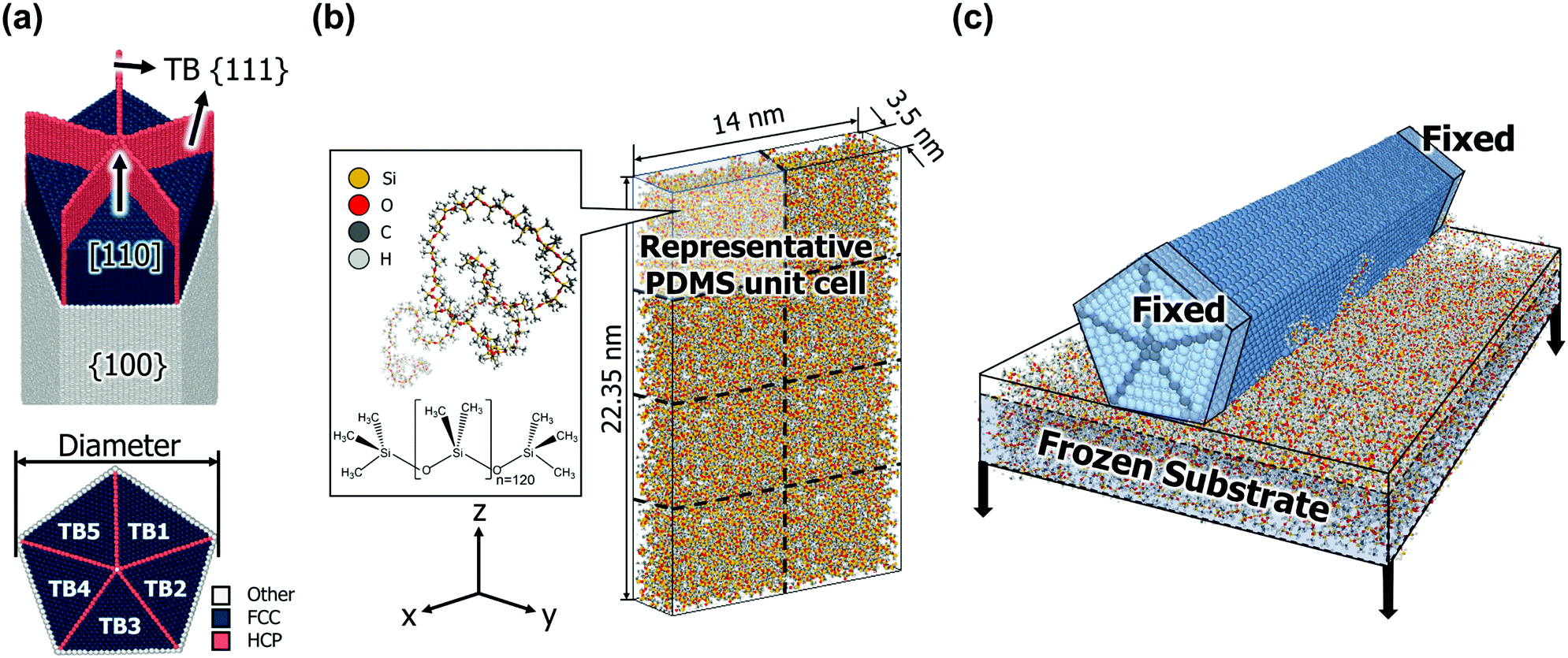 | ||
| Fig. 1 All-atom structural model used in this study. (a) [110]-oriented penta-twinned AgNW with {111} TBs and {100} free surfaces (up) and cross-section with twin variants of TB1–TB5 (down); (b) structure of the PDMS substrate. An amorphous PDMS unit cell containing eight polymer chains is first modelled, and the entire substrate is constructed by replicating the PDMS unit cell twice along the x-axis and four times along the z-axis. (c) Bow deformation model of an AgNW on a PDMS substrate. | ||
The geometries of the considered AgNWs are listed in Table 1. The models are classified by the diameter of the NWs, which range from 2.80 nm to 6.53 nm. The lengths in the z direction are the same (22.35 nm). Each diameter model is replicated in the [110] axial direction to make the aspect ratio in the unit cell range from a minimum of 3.42 to a maximum of 17.97.
| Diameter (nm) | Length (nm) | Aspect ratio (L/d) |
|---|---|---|
| 2.80 | 22.35 | 7.98 |
| 3.73 | 5.99 | |
| 4.67 | 4.78 | |
| 6.53 | 3.42 | |
| 3.73 | 44.70 | 11.98 |
| 4.67 | 9.57 | |
| 6.53 | 6.84 | |
| 3.73 | 67.05 | 17.97 |
| 4.67 | 14.35 | |
| 6.53 | 10.26 |
The interaction between Ag atoms was defined as an embedded atom method (EAM) potential.37 The total energy, Etot, is given by
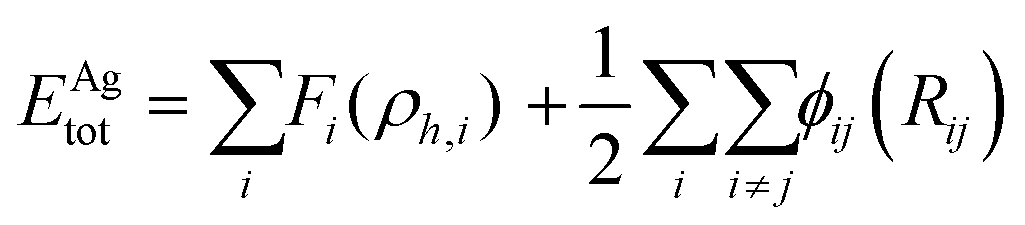 | (1) |
For the structural relaxation of each modelled nanowire, an NVT ensemble simulation with a periodic boundary condition along the z direction was performed at 300 K for 2 ns, which resulted in the embodiment of the infinite length condition. Subsequently, an NPT ensemble simulation was conducted at 300 K and 0.1 MPa for 2 ns to determine the effective unit length of the AgNW model. A timestep of 1 fs was applied, and the equations of motion were integrated using the Verlet algorithm. Note that the validity of the potential used in this study was assessed by uniaxial tensile load testing of the AgNWs. The size-dependent mechanical properties of the AgNWs as well as the phase transformation associated with stacking fault decahedron (SFD) were successfully reproduced as reported in previous studies (see Fig. S1 and S2, ESI†). Accordingly, the force field selection for AgNWs is considered appropriate within the range of mechanical properties covered in this study.
The polydimethylsiloxane (PDMS) substrate was defined as a polymer consistent force field (PCFF) potential, where the total energy (Etot) is described as38
| EPDMStot = Ebond + Eangle + Etorsion + Eoop + Ecross + EvdW + ECoulombic | (2) |
Fig. 1b shows the PDMS substrate model used in this study. Each single PDMS chain contains 120 repeated units, and the representative unit cell consists of the eight PDMS chains in an amorphous state. To achieve natural entanglement while avoiding unexpected interference between chains, the allocation of the initial chain positions was performed under the condition of a low density of 0.2 g cc−1. Subsequently, the density of the unit cell was gradually increased while preserving the periodic boundary conditions in all directions. The process continued until the density of the unit cell reached an experimentally determined value (0.965 g cc−1).40 The density was increased by reducing the length of the unit cell box while maintaining the fractional coordinates of all atoms. When the density of the system increased by 0.2 g cc−1 (0.165 g cc−1 in the last stage), the potential energy was minimized using the conjugated gradient method.
For the structural relaxation of the modelled PDMS unit cell, an NVT ensemble simulation at 300 K for 1 ns and an NPT ensemble simulation at 300 K and 0.1 MPa for 1 ns were conducted sequentially with the timestep of 1 fs. The temperature, density, and energy convergence profiles of the NPT simulations are shown in Fig. S3 (ESI†). The density is converged to 0.971 g cc−1 at 300 K, which is very close to the desired density. A PDMS substrate model in contact with an AgNW was constructed by replicating the PDMS unit cell. The unit cell was replicated twice along the x-axis and four times along the z-axis; therefore, the size of the substrate was 14 × 3.5 × 22.35 nm.3 The PDMS substrate model was replicated once more in the z direction up to 3 times according to the length of the AgNW model.
The equilibrated PDMS substrate and AgNW models were attached together, which is depicted in Fig. 1c. First, a very thick vacuum layer (more than 14 nm depending on the model) was inserted in the y direction of the PDMS model to secure a space for the AgNW. To relax the surface stress of the PDMS substrate, an NVT ensemble at 300 K was applied for 1 ns with the timestep of 1 fs to the upper 20% area of the substrate. Subsequently, the AgNW was aligned ∼5 Å above the substrate surface while maintaining the periodic boundary conditions in the x and z directions, and applied an NVT ensemble simulation at 300 K for 1 ns with the timestep of 0.5 fs. After the two components were in contact, 5 Å of the regions at both ends of the AgNW were clamped, whereas the lower 80% area of the PDMS (defined as the frozen substrate region in Fig. 1c) was pulled in the y direction. Delamination simulations were carried out under the NVT ensemble at 0.1 K with a timestep of 0.5 fs, and the pull-out speed of the substrate was set as 1 m s−1. It was confirmed that the given pull-out rate of PDMS can suitably produce the quasi-static behaviour experienced by the AgNWs (Fig. S4, ESI†).
The atomic interaction between the Ag and PDMS constituent atoms was described by the 9–6 Lennard-Jones potential (ELJ), which is expressed as follows:
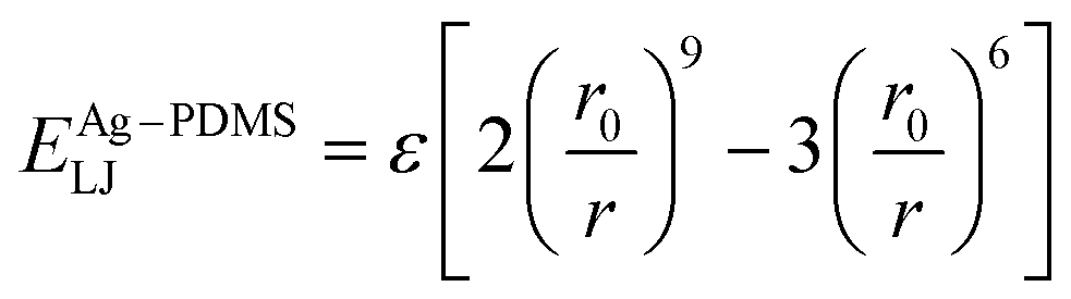 | (3) |
Results and discussion
Fig. 2a shows the mechanical behaviour of a representative AgNW (diameter of 4.67 nm and aspect ratio of 4.78) in bow deformation and recovery. The nanowire experienced a large deformation at approximately 13% strain, but then returned to its original position without fracture during the detachment of the PDMS substrate. Three critical points are indicated by arrows in Fig. 2a. The first point (point A) corresponds to the yielding when an initial dislocation nucleation occurs.43 After the yielding of the AgNW, many dislocations nucleate and start to slip at the TBs. As the strain increases further, dislocations cut across the TBs, and slips are triggered by partial dislocation nucleation.24 At the second point (point B), the AgNW undergoes maximum displacement, whereas the dislocations begin to diminish. The Peach–Koehler force, a repulsive force between TBs and a curved dislocation loop, acts on the dislocations and causes the intrinsic force field to promote the retraction of the dislocations.44 The resultant dislocations at large deformations start to retract back, which results in strain recovery. The last point (point C) corresponds to the equilibrium structure after the strain recovery is complete. Upon unloading, several dislocations do not fully return to their initial locations. The stacking fault decahedron (SFD) also disappears, but the stage leaves sessile dislocations at the TBs and hinders the complete recovery of the plastic deformation. Such an imperfect release of bending stress is also in good agreement with the unbending response of a five-fold AgNW demonstrated by Schrenker et al.26 However, we focused on the fact that the present AgNW model consists of TBs having a coherent atomic structure, low energy, and high symmetry. The nucleated dislocations are blocked by the TBs, which not only play a role in strain hardening but also act as barriers to dislocations. Such dislocation–TB interactions allow the diffusion and sliding processes to be significantly suppressed, suggesting a reversible plastic strain recovery behaviour upon unloading. Specifically, the residual stress remaining in the AgNW after the PDMS delamination can be almost completely removed, depending on the shape of the AgNW. This will be discussed in more detail in the next section on the results for various D and AR changes of the AgNWs. Fig. 2b shows the atomic structure of the above-mentioned representative AgNW when it reaches the maximum strain. Multiple permanent defects remain, particularly in the central region and both ends of the AgNW, which experience the largest strain. The contact area between the AgNW and PDMS reduces as the PDMS substrate is detached, and only the central part of the AgNW interacts with PDMS until the end.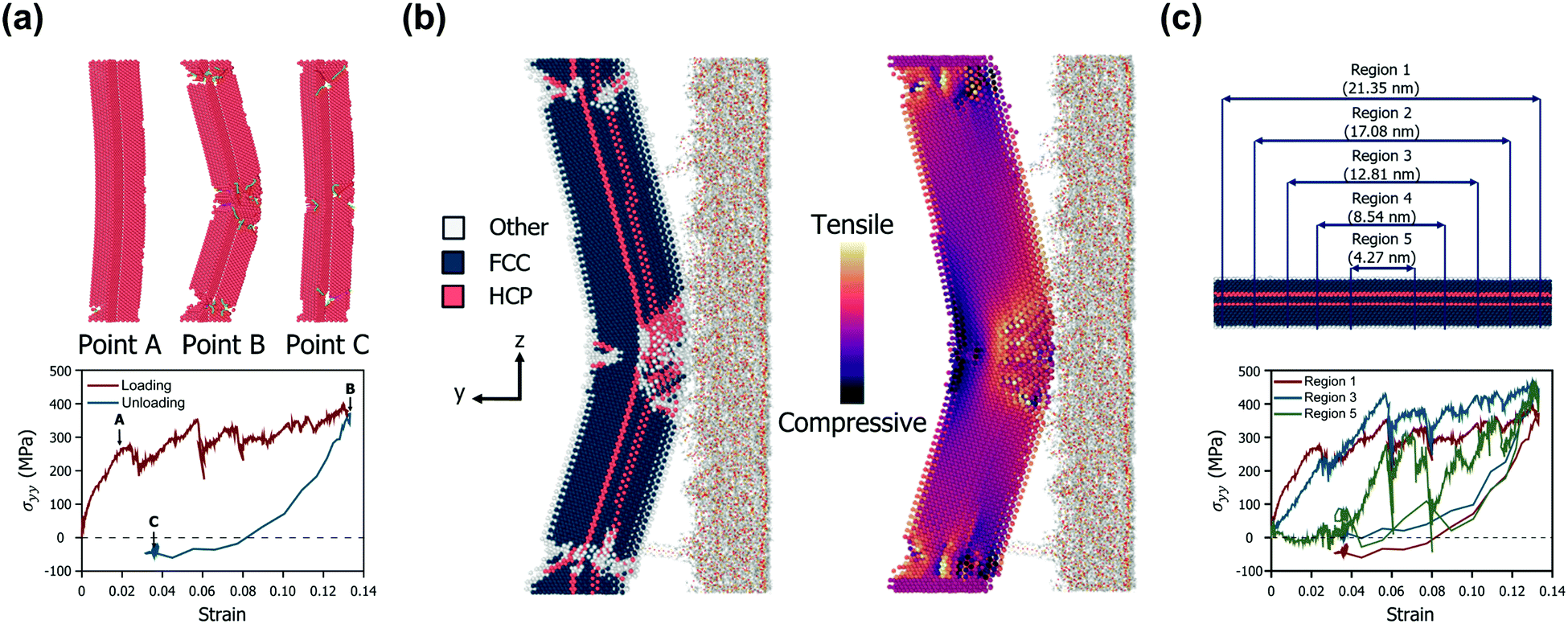 | ||
| Fig. 2 Bow deformation and subsequent recovery behaviour experienced by an AgNW with diameter of 4.67 nm and aspect ratio of 4.78 during detachment from the PDMS substrate. (a) Overall stress–strain curve in the y direction (down) and key snapshots of atomic structure and dislocations are depicted (up). For clarification, only the hexagonal close packed structure is presented. (b) Internal crystal structure and atomic stress distribution of the σzz component when the AgNW experiences maximum strain. (c) Subdivision regions in the undeformed AgNW and profiles of σyy during detachment from the PDMS substrate. | ||
Thus, many dislocations nucleate and propagate in the center of the AgNW, followed by the largest deformation.
Meanwhile, the normal stress distribution along the AgNW is depicted on the right in Fig. 2b. The stress tensor of the AgNW (σij) during the bow deformation is calculated using the virial theorem expressed in eqn (4).45
 | (4) |
In order to further analyse the intrinsic stress distribution of the AgNW from a volumetric point of view, we set subdivision regions by length as depicted in Fig. 2c. The profiles of the average value of σyy for each region during the detachment process are shown in the lower part of Fig. 2c.
Under the condition of a small strain of less than 0.02, the magnitude of the stress component is measured to be smaller as the observation area becomes closer to the center of the AgNW. This suggests that most of the stress concentration occurs at both ends of the AgNW in an environment where all regions of the AgNW fully interact with the PDMS substrate. This also agrees well with the result that the first partial dislocation occurs at both ends of the AgNW. However, as the deformation continues, the effective region of the stress-resisting detachment and the resulting plastic deformation extend to the central region of the AgNW. When the maximum strain is reached, only the region belonging to the center of the AgNW directly interacts with the PDMS, and thus, the maximum stress occurs in this region. Finally, after the PDMS substrate is completely peeled off, a permanent strain of approximately 3% remains in the AgNW, and the residual stress for each region is highly distributed. The changes in the stress distributions of all AgNW models during the bow deformation and the subsequent separation from the PDMS substrate are shown in Video S1 (ESI†).
The rupture point caused by the bow deformation behaviour of each AgNW could be precisely identified by the change in the interfacial energy formed with PDMS. The interfacial energy density (Γint) between each AgNW and the PDMS substrate is calculated as follows:
| Γint = (Utotal − (UAg + UPDMS))/A | (5) |
 | ||
| Fig. 3 (a) Illustration of the interfacial energy density (left) formed at the contact region (right) during PDMS separation. (b) Stress–strain curves of AgNWs with a length of 67.04 nm during bow deformation and (c) corresponding interfacial energy density profiles. (d) Representative snapshots when each AgNW experiences maximum strain. | ||
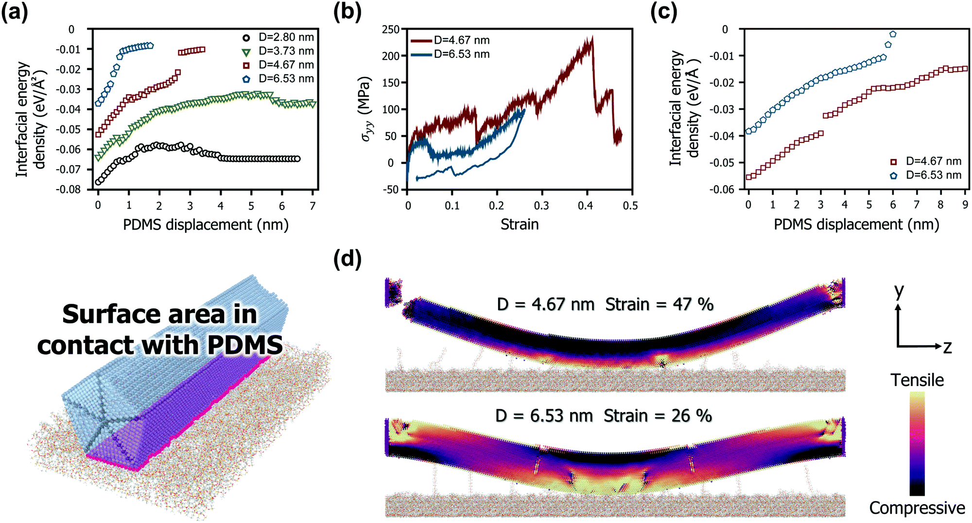
The differences in the bow deformation behaviour according to the geometries of the AgNWs were more closely explored from a structural perspective. Fig. 3b shows the mechanical behaviour of two representative AgNWs with a length of 67.04 nm (diameters of 4.67 nm and 6.53 nm, resulting in aspect ratios of 14.36 and 10.26, respectively). For the AgNW with a diameter of 4.67 nm, dislocations begin to form at both ends as the strain reaches 0.3, whereas the middle region retains the pristine structure. As the strain progresses further and reaches 0.47, a severe tensile stress is locally generated on one side of both ends, causing one end to fracture. On the other hand, the AgNW with a diameter of 6.53 nm is completely separated from the PDMS before the axial stress reaches 100 MPa and returns to its original position.
Such a difference is also clearly observed through the interfacial energy densities based on the change in the effective area of the AgNWs in contact with PDMS, as depicted in Fig. 3c. For the AgNW with a diameter of 6.53 nm, its interaction energy with PDMS rapidly decreases as the PDMS displacement exceeds 6 nm. However, for the AgNW with a diameter of 4.67 nm, the contact area with PDMS is maintained high during the entire deformation. Therefore, the rate of decrease in the interaction energy density according to displacement is relatively low. In particular, as the AgNW that failed to transfer along with the fracture return to the PDMS surface, the interfacial energy density is rather slightly recovered.
Fig. 3d shows the internal stress distribution at the moment each AgNW experiences the maximum strain. Note that the snapshots show the point of failure for the 4.67 nm diameter model and the maximum stress point for the 6.53 nm diameter model. First, the results for the case of the 4.67 nm in diameter model suggest that the central contact area with PDMS is very wide over all periods. This is due to the strong interaction energy density of the small diameter AgNWs, as shown in Fig. 3a and c. Good adherence to the PDMS substrate causes both ends of the nanowire to undergo a large angular strain during bow deformation, causing stress concentration. While tensile stress is concentrated at both ends, compressive stress is evenly distributed in most areas of the nanowire, and thus, fracture is triggered only by the tensile stress. Another interesting finding is that no phase transformation was observed in the region in contact with the PDMS substrate at the moment of fracture. Accordingly, the ruptured AgNW has few defects in the middle region. In contrast, the edges of the 6.53 nm diameter model show no fractures despite many dislocations and defects. The AgNW under this condition not only has a sufficiently small bending strain but also forms V-shaped defects in the middle region. The defects significantly relieve the internal stress by changing the bending moment at the middle region to kink deformation. Consequently, neither end of the nanowire is subjected to a large angular strain. In particular, as shown In Fig. 2b, these V-shaped defects are almost completely eliminated, and the AgNW almost returns to its pristine state by strain recovery after the separation of PDMS. The stress contour generated by the tensile and compressive stresses during bow deformation is also properly distributed in balance.
Experimental validation of the proposed AgNW transfer process was achieved by the successive application of the laser-induced photothermal bonding technique, which was recently developed by our group.33 In a typical experiment, as shown in Fig. 4a, AgNWs (D: 66.1–149 nm, length: 100–200 μm, ACS Material) dispersed in ethanol at 0.033 wt% were firstly deposited on a PDMS donor substrate by drop casting. Subsequently, the PDMS donor substrate is attached to an acceptor polyimide (PI) film by a motorized linear stage. The two ends of the target AgNW are then exposed to a 532 nm wavelength continuous-wave laser (Sprout-G-5 W, Lighthouse Photonics) focused by a 5× objective lens at 90 mW power for 100 ms to enhance the adhesion between PDMS and PI in a spatially selective manner. The laser-induced bonding switches the adhesive failure between PI and PDMS to a cohesive failure within PDMS.33 Thus, both ends of the Ag NW are effectively anchored to the PI film immediately after the laser exposure, providing analogous boundary conditions employed in the MD simulations. Therefore, we anticipate that the AgNW experiences bow deformation upon the detachment step, as shown in the schematics. A real-time movie clip of the entire transfer process is included in Video S2 (ESI†). The success or failure of the proposed process is determined by the transfer characteristics of the middle section of the target AgNW which is not subject to the laser exposure. Optical microscopy (BX53M, Olympus) images of two representative cases are shown in Fig. 4b and c. The successful transfer enables precise relocation of the entire AgNWs to the acceptor substrate without any observable damage (Fig. 4b). In contrast the AgNW experiences failure to abandon the middle section of the PDMS donor substrate if the distance between the two laser exposures exceeds a certain threshold value (Fig. 4c). The disconnection of the AgNW is frequently found in the vicinity of the anchoring points that experience the maximum tensile stress, as predicted from the simulations. A closer examination of the transferred AgNWs with SEM (JSM-7600f, JEOL and MIRA3, Tescan) and energy-dispersive X-ray spectroscopy (EDS), on the other hand, showed no signs of significant structural deformation (Fig. 4d) or alteration in elemental composition, brightening the prospect of the proposed process as a facile transfer technique for a single AgNW. Due to the unique transfer mechanism proposed in this study, the maximum length of the AgNW that is transferrable by the proposed process is limited, depending on the diameter of the corresponding AgNW, as validated by both simulations and experiments.
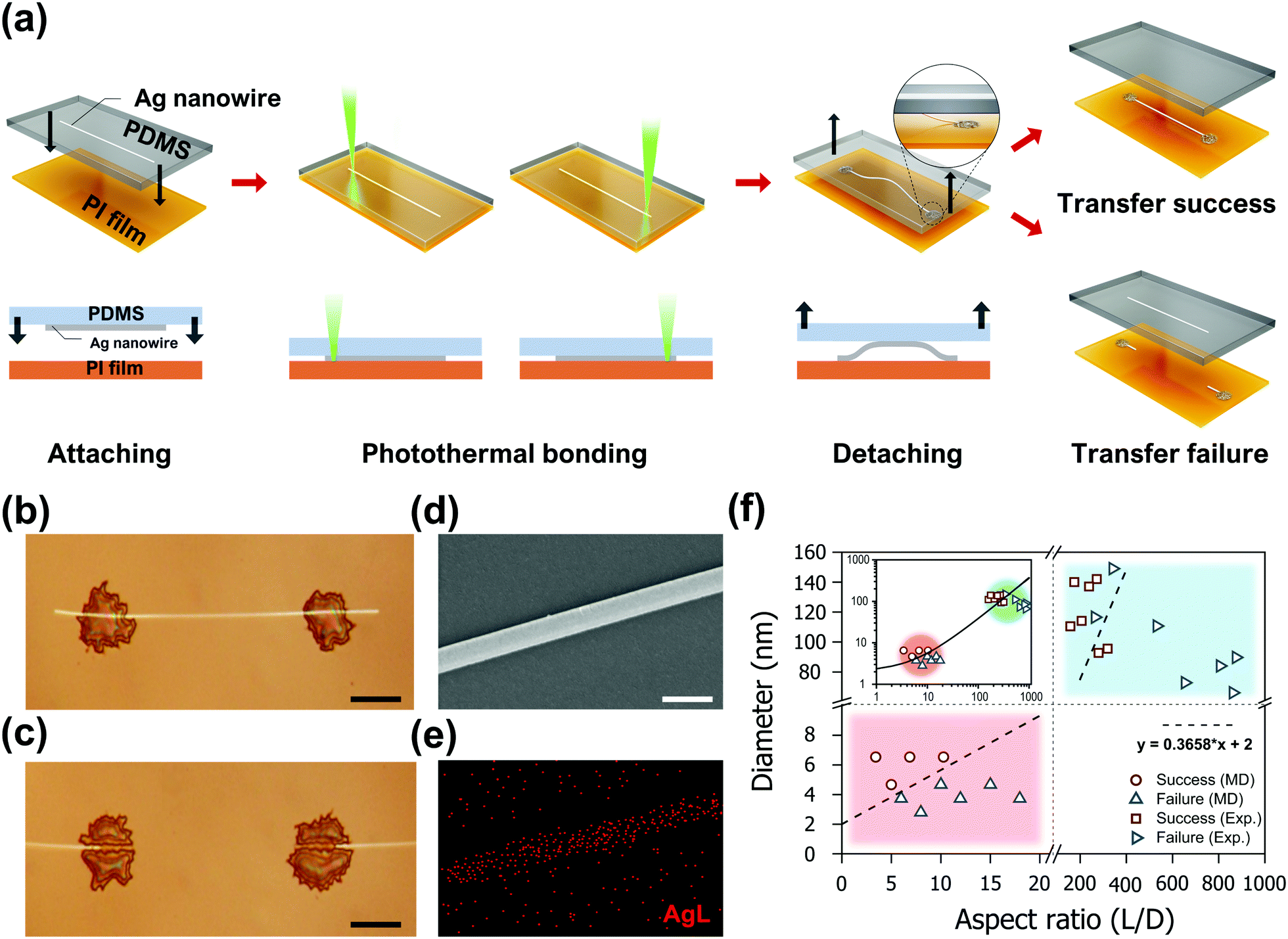 | ||
| Fig. 4 (a) Schematic flow (top) and front view (bottom) of the laser-induced AgNW transfer process. Optical microscopy images of each sample when the transfer process (b) succeeds and (c) fails (scale bar: 5 μm). (d) Close-up SEM image of the sample after a successful transfer process (scale bar: 250 nm). (e) EDS mapping of the Ag element corresponding to image (d). (f) Transfer process success/failure model that integrates MD simulation results and experimental observations (not breaks in axes). Inset plots are fitting data in log–log scales. | ||
On the basis of the MD simulation results and the experimental findings, an empirical model considering the shape parameter of the AgNWs for the transfer process was proposed. For the assessment of the transferrable length, the simulation and experimental results are plotted simultaneously, as shown in Fig. 4f. Subsequently, a linear estimation condition was found that distinguishes the success and failure of the laser-induced transfer process. Despite the significant dimensional difference between the MD simulations and the experiments, the fitted line predicts the success or failure of the process with high precision, except for a few experimental values in the transient region. Also refer to the inset of Fig. 4f for the regression results plotted combinedly on a log–log scale. From a quantitative perspective, the model suggests that AgNWs with a diameter of 100 nm can be transferred to a length of ∼20 μm. This is an important finding as it demonstrates that single AgNWs with dimensions usable as ultra-small electrodes can be fabricated by the laser transfer process.49
Conclusions
In conclusion, in this study, the bow deformation behaviour of single penta-twinned AgNWs attached to PDMS substrates was investigated. The structural and interfacial stabilities of the AgNWs were evaluated through MD simulations by calculating the stress distribution generated by the laser irradiation process. The process results according to the diameters and aspect ratios of the AgNWs were systematically analysed from the virial stress and the interfacial energy density. The AgNW transfer process following laser irradiation of PDMS was realized in experiments. Based on the MD simulation results and the experimental observations, an empirical model of the transfer process considering the AgNW geometry was established.So far, many experimental studies have been reported on the change in the adhesion strength of metallic nanomaterials with polymeric surfaces by laser irradiation. However, there have been no systematic studies on the mechanical stress experienced by nanomaterials during the transfer process and their critical structures. The present study is the first attempt to systematically understand the transfer process of a single AgNW at the interface between dissimilar materials. The mechanisms of dislocation nucleation, propagation and slip occurring inside the AgNW during the detachment of the PDMS substrate were also successfully characterized. In particular, the results suggested that for AgNWs with specific dimensions, the phase change can be elastically restored to the original state with complete separation of PDMS. The phase transformation caused by dislocation–TB interactions was reversibly released as the nucleated dislocations were blocked and retracted by the TBs.
This finding can be further extended to the mechanical design of nanowire electrodes where internal defects and transformations significantly affect the overall performance. By minimizing the structural damage of the AgNW involved in the transfer process, single nanowire electrode devices can be fabricated without loss of conductivity. Several other efforts are also underway to assess the effect of the bidirectional interaction between the donor and acceptor substrates, improvement in the adhesive strength due to the physicochemical surface treatment of the donor substrate, and imperfect bonding effect at the edge of the nanowire.
Author contributions
Minseok Kang: methodology, software, visualization, writing – original draft. Hyunkoo Lee: methodology, validation. Sukjoon Hong: conceptualization, supervision, writing – review & editing Joonmyung Choi: conceptualization, supervision, writing – review & editing.Conflicts of interest
The authors declare that they have no known competing financial interests or personal relationships that could have appeared to influence the work reported in this paper.Acknowledgements
This research was supported by the National R&D Program of the National Research Foundation of Korea (NRF) (2022R1F1A1063199, 2022R1C1C1006593). Also, this work was supported by the research fund of Hanyang University (HY-2021-2594).References
- F. Xu and Y. Zhu, Adv. Mater., 2012, 24, 5117–5122 CrossRef CAS PubMed.
- Y. Zhu, Q. Qin, F. Xu, F. Fan, Y. Ding, T. Zhang, B. J. Wiley and Z. L. Wang, Phys. Rev. B: Condens. Matter Mater. Phys., 2012, 85, 045443 CrossRef.
- S. De, T. M. Higgins, P. E. Lyons, E. M. Doherty, P. N. Nirmalraj, W. J. Blau, J. J. Boland and J. N. Coleman, ACS Nano, 2009, 3, 1767–1774 CrossRef CAS PubMed.
- A. R. Madaria, A. Kumar and C. Zhou, Nanotechnology, 2011, 22, 245201 CrossRef PubMed.
- X.-Z. Xiang, W.-Y. Gong, M.-S. Kuang and L. Wang, Rare Met., 2016, 35, 289–298 CrossRef CAS.
- J. Chavalitkul, O. Margeat, J. Ackermann and S. T. Dubas, Thin Solid Films, 2020, 711, 138272 CrossRef CAS.
- S. Kang, T. Kim, S. Cho, Y. Lee, A. Choe, B. Walker, S.-J. Ko, J. Y. Kim and H. Ko, Nano Lett., 2015, 15, 7933–7942 CrossRef CAS PubMed.
- J. Lee, P. Lee, H. B. Lee, S. Hong, I. Lee, J. Yeo, S. S. Lee, T.-S. Kim, D. Lee and S. H. Ko, Adv. Funct. Mater., 2013, 23, 4171–4176 CrossRef CAS.
- H.-G. Im, J. Jin, J.-H. Ko, J. Lee, J.-Y. Lee and B.-S. Bae, Nanoscale, 2014, 6, 711–715 RSC.
- A. C. Myers, H. Huang and Y. Zhu, RSC Adv., 2015, 5, 11627 RSC.
- M. Lagrange, D. P. Langley, G. Giusti, C. Jiménez, Y. Bréchet and D. Bellet, Nanoscale, 2015, 7, 17410 RSC.
- C. Mayousse, C. Celle, A. Fraczkiewicz and J.-P. Simonato, Nanoscale, 2015, 7, 2107 RSC.
- S. Park, A. W. M. Tan, J. Wang and P. S. Lee, Nanoscale Horiz., 2017, 2, 199 RSC.
- A. Tao, F. Kim, C. Hess, J. Goldberger, R. He, Y. Sun, Y. Xia and P. Yang, Nano Lett., 2003, 3, 1229–1233 CrossRef CAS.
- S. Shanmukh, L. Jones, J. Driskell, Y. Zhao, R. Dluhy and R. A. Tripp, Nano Lett., 2006, 6, 2630–2636 CrossRef CAS PubMed.
- J. Jung, H. Cho, R. Yuksel, D. Kim, H. Lee, J. Kwon, P. Lee, J. Yeo, S. Hong, H. E. Unalan, S. Han and S. H. Ko, Nanoscale, 2019, 11, 20356 RSC.
- X. Liang, T. Zhao, W. Jiang, X. Yu, Y. Hu, P. Zhu, H. Zheng, R. Sun and C.-P. Wong, Nano Energy, 2019, 59, 508–516 CrossRef CAS.
- S. Cho, S. Kang, A. Pandya, R. Shanker, Z. Khan, Y. Lee, J. Park, S. L. Craig and H. Ko, ACS Nano, 2017, 11, 4346–4357 CrossRef CAS PubMed.
- L. Hu, H. S. Kim, J.-Y. Lee, P. Peumans and Y. Cui, ACS Nano, 2010, 4, 2955–2963 CrossRef CAS PubMed.
- Q. Che, Q. Zhao, M. Hu, R. Qin, G. Shan and J. Yang, ACS Appl. Nano Mater., 2021, 4, 12726–12736 CrossRef CAS.
- S. Vlassov, B. Polyakov, L. M. Dorogin, M. Antsov, M. Mets, M. Umalas, R. Saar, R. Lõhmus and I. Kink, Mater. Chem. Phys., 2014, 143, 1026–1031 CrossRef CAS.
- S. E. H. Murph, C. J. Murphy, A. Leach and K. Gall, Cryst. Growth Des., 2015, 15, 1968–1974 CrossRef.
- H. Zhao, A. S. Eggeman, C. P. Race and B. Derby, Acta Mater., 2020, 185, 110–118 CrossRef CAS.
- T. Filleter, S. Ryu, K. Kang, J. Yin, R. A. Bernal, K. Sohn, S. Li, J. Huang, W. Cai and H. D. Espinosa, Small, 2012, 8, 2986–2993 CrossRef CAS PubMed.
- D. Kim, S.-H. Kim, J. H. Kim, J.-C. Lee, J.-P. Ahn and S. W. Kim, Sci. Rep., 2017, 7, 45903 CrossRef CAS PubMed.
- N. J. Schrenker, Z. Xie, P. Schweizer, M. Moninger, F. Werner, N. Karpstein, M. Mačković, G. D. Spyropoulos, M. Göbelt, S. Christiansen, C. J. Brabec, E. Bitzek and E. Spiecker, ACS Nano, 2021, 15, 362–376 CrossRef CAS PubMed.
- K. Cao, Y. Han, H. Zhang, L. Gao, H. Yang, J. Chen, Y. Li and Y. Lu, Nanotechnology, 2018, 29, 295703 CrossRef PubMed.
- J. Cuny, N. Tarrat, F. Spiegelman, A. Huguenot and M. Rapacioli, J. Phys.: Condens. Matter, 2018, 30, 303001 CrossRef PubMed.
- N. V. Ilawe, M. B. Oviedo and B. M. Wong, J. Mater. Chem. C, 2018, 6, 5857 RSC.
- Z. Liu, M. B. Oviedo, B. M. Wong and C. M. Aikens, J. Chem. Phys., 2022, 156, 154705 CrossRef CAS PubMed.
- L. F. L. Oliverira, N. Tarrat, J. Cuny, J. Morillo, D. Lemoine, F. Spiegelman and M. Rapacioli, J. Phys. Chem. A, 2016, 120, 8469–8483 CrossRef PubMed.
- J. Lim, Y. Kim, J. Shin, Y. Lee, W. Shin, W. Qu, E. Hwang, S. Park and S. Hong, Nanomaterials, 2020, 10, 701 CrossRef CAS PubMed.
- J. Lim, B. Goh, W. Qu, Y. Kim, J. Choi and S. Hong, Appl. Surf. Sci., 2022, 571, 151123 CrossRef CAS.
- P. Sopeña, P. Serra and J. M. Fernández-Pradas, Appl. Surf. Sci., 2019, 476, 828–833 CrossRef.
- Y. Gao, L. Song, P. Jiang, L. F. Liu, X. Q. Yan, Z. P. Zhou, D. F. Liu, J. X. Wang, H. J. Yuan, Z. X. Zhang, X. W. Zhao, X. Y. Dou, W. Y. Zhou, G. Wang, S. S. Xie, H. Y. Chen and J. Q. Li, J. Cryst. Growth, 2005, 276, 606–612 CrossRef CAS.
- J. Monk, J. J. Hoyt and D. Farkas, Phys. Rev. B: Condens. Matter Mater. Phys., 2008, 78, 024112 CrossRef.
- S. M. Foiles, M. I. Baskes and M. S. Daw, Phys. Rev. B: Condens. Matter Mater. Phys., 1986, 33, 7983–7991 CrossRef CAS PubMed.
- H. Sun, J. Comput. Chem., 1994, 15, 752–768 CrossRef CAS.
- R. W. Hockney and J. W. Eastwood, Computer Simulation Using Particles, Taylor & Francis, 1989 Search PubMed.
- S. T. Choi, B. S. Son, G. W. Seo, S.-Y. Park and K.-S. Lee, Opt. Express, 2014, 22, 6133–6146 CrossRef PubMed.
- S. Plimpton, J. Comput. Phys., 1995, 117, 1–19 CrossRef CAS.
- A. Stukowski, Modell. Simul. Mater. Sci. Eng., 2010, 18, 015012 CrossRef.
- R. A. Bernal, A. Aghaei, S. Lee, S. Ryu, K. Sohn, J. Huang, W. Cai and H. Espinosa, Nano Lett., 2015, 15, 139–146 CrossRef CAS PubMed.
- Q. Qin, S. Yin, G. Cheng, X. Li, T.-H. Chang, G. Richter, Y. Zhu and H. Gao, Nat. Commun., 2015, 6, 5983 CrossRef CAS PubMed.
- D. M. Heyes, Phys. Rev. B: Condens. Matter Mater. Phys., 1994, 49, 755 CrossRef CAS PubMed.
- T. Radetic, F. Lancon and U. Dahmen, Phys. Rev. Lett., 2002, 89, 085502 CrossRef CAS PubMed.
- G.-S. Liu, C. Liu, H.-J. Chen, W. Cao, J.-S. Qiu, H.-P. D. Shieh and B.-R. Yang, Nanoscale, 2016, 8, 5507–5515 RSC.
- G.-S. Liu, J.-S. Qiu, D.-H. Xu, X. Zhou, D. Zhong, H.-P. Shieh and B.-R. Yang, ACS Appl. Mater. Interfaces, 2017, 9, 15130–15138 CrossRef CAS PubMed.
- A. Heinzig, S. Slesazeck, F. Kreupl, T. Mikolajick and W. N. Weber, Nano Lett., 2012, 12, 119–124 CrossRef CAS PubMed.
Footnote |
| † Electronic supplementary information (ESI) available. See DOI: https://doi.org/10.1039/d2nh00212d |
| This journal is © The Royal Society of Chemistry 2022 |