
Patterning submicron photomechanical features into single diarylethene crystals using electron beam lithography†
Wangxiang
Li
 a,
Daichi
Kitagawa
b,
Seiya
Kobatake
b,
Elena
Bekyarova
a and
Christopher J.
Bardeen
*a
a,
Daichi
Kitagawa
b,
Seiya
Kobatake
b,
Elena
Bekyarova
a and
Christopher J.
Bardeen
*a
aDepartment of Chemistry, University of California, Riverside, 501 Big Springs Road, Riverside, CA 92521, USA. E-mail: christopher.bardeen@ucr.edu
bDepartment of Applied Chemistry, Graduate School of Engineering, Osaka City University, 3-3-138 Sugimoto, Sumiyoshi-ku, Osaka, 558-8585, Japan
First published on 20th June 2022
Abstract
Lithography methods are commonly used to create structures in inorganic semiconductors like silicon but have not been widely applied to organic crystals. In this work, electron beam lithography (EBL) is used to pattern structures into single organic photomechanical crystals composed of 1,2-bis(2-methyl-5-phenyl-3-thienyl)perfluorocyclopentene. The electron beam creates amorphous regions of decomposed molecules, while the reactivity of the unexposed crystal regions is preserved under a removable Au coating. Exposure of the patterned crystal to 365 nm light causes ridges of amorphous material to increase in height by 30–70%. This height increase can be reversed by visible light exposure and undergo multiple cycles. The reversible surface morphology changes are strong enough to rupture a sheet of graphene placed on top of the patterned crystal. Surprisingly, the change in dimensions of the EBL features is an order of magnitude larger than the changes in overall crystal dimensions as deduced from X-ray diffraction experiments and microscopy observations. A dynamic extrusion model is presented to explain how nanoscale features imprinted into single crystals can amplify molecular-level photomechanical changes. This work demonstrates the capability of EBL methods to produce sub-micron structural features on single photomechanical crystals, providing a new route to monolithic light-powered actuator devices.
Introduction
The semiconductor industry uses optical and electron beam lithography to precisely place nanoscale features into high purity single crystals of silicon.1 The advantage of this top-down approach is that the desirable features of a single crystal, like high charge carrier and exciton mobilities, can be distributed across many smaller functionalities. Organic electronic materials exhibit a similar trend, in that the highest performance tends to originate from single crystal devices. Interestingly, this field has concentrated on the growth of arrays of single crystals,2–4 each functioning in a stand-alone device, rather than integrating multiple elements onto a single crystal. It is an open question as to whether it is possible to use lithography techniques to create functional units across a single organic crystal, similar to what is done for silicon crystals.While the technology for creating features in inorganic crystals is well-developed, the solubility of molecular crystals in organic solvents precludes the use of standard photoresist techniques. The creation of surface patterns using photolithography on polymers is well-established,5 and techniques have been developed to deposit metal patterns on molecular crystals as well.6 In order to modify the underlying crystal structure, focused ion beam7,8 and electron beam methods9–15 have been successfully used to pattern nano- and microscale features into organic and organometallic molecular solids. For cocrystals incorporating a volatile component, light can also be used to carve features into single crystals.16 These patterned structures are generally passive, for example waveguides and gratings that modulate the light emission of optoelectronic devices. The creation of active microscale structures in single organic crystals has not been demonstrated to our knowledge. Active electronic elements like transistors, present special challenges since they would require spatial control of doping. But the creation of simpler physical features, like trenches or islands, could be useful if the crystal itself was composed of an active material. For example, photomechanical crystals composed of molecules that undergo photoisomerization can undergo mechanical deformations in response to light exposure.17–20 Lithographically defined features in such crystals could give rise to patterned surface shape changes upon light exposure, similar to what has been observed in polymers and gels.21–28
The reversible diarylethene ring-open to ring-closed electrocyclization shown in Scheme 1 is an example of a photochemical reaction that has been harnessed for photomechanical actuation.29–34 Single microcrystals can undergo anisotropic expansions that generate substantial forces.35 To create macroscopic actuator structures based on this photochromism, we recently developed a bottom-up approach that assembled crystalline diarylethene nanowires inside a porous ceramic host material.36,37 This approach was successful in generating useful mechanical motion, e.g. tilting mirrors, but variations in the template quality and filling made the production of reproducible samples a challenge. Moreover, recent work suggests that the nanowire morphology may lack the fatigue resistance and mechanical robustness seen in larger single crystals.38 The creation of actuator structures in monolithic single crystals could avoid these problems while exhibiting higher fatigue resistance and/or larger force generation.
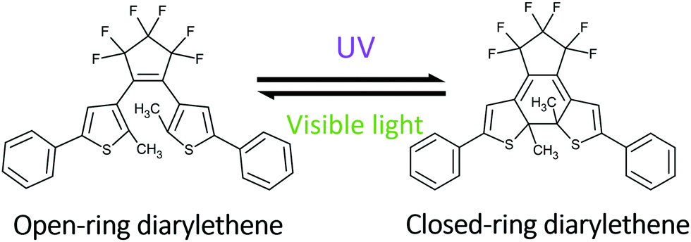 | ||
| Scheme 1 Reversible photochemical reaction between open-ring and closed-ring isomers of 1,2-bis(2-methyl-5-phenyl-3-thienyl)perfluorocyclopentene (DAE). | ||
The goal of this paper is to illustrate the use of electron beam lithography (EBL) to create actuator structures in single crystals that exhibit reversible mechanical motion. The substrate crystal is composed of 1,2-bis(2-methyl-5-phenyl-3-thienyl)perfluorocyclopentene, whose structure is shown in Scheme 1 and referred to as DAE in this paper. EBL is used to create amorphous regions of decomposed DAE molecules, while the reactivity of the unexposed regions is preserved under a removable Au coating. Exposure of the patterned crystal to ultraviolet (UV) light causes ridges of amorphous material to increase in height by ∼50%, and this height increase can be reversed by visible light exposure. Remarkably, the change in dimensions of the EBL features is an order of magnitude larger than the changes in overall crystal dimensions as deduced from X-ray diffraction experiments and microscopy observations. We present a model for how nanoscale features imprinted into single crystals can amplify the molecular-level photomechanical changes. This work shows that nanoscale patterning of single photomechanical crystals provides a route to light-powered devices with precise structural features. These chip-scale photomechanical devices could have applications as optomechanical elements or micromachines.
Results and discussion
The challenge in patterning an organic crystal using EBL is to avoid damaging the entire crystal with the high energy electrons. If the intramolecular bonds of the DAE are broken by electron impact, the molecules will no longer be able to undergo photoisomerization. If the intermolecular bonds are disrupted, crystalline order will be lost and there will no longer be a coordinated, macroscopic mechanical response. To protect the crystal, we encapsulated it with a 5 nm Au layer to avoid accumulation of charge during electron beam scanning and imaging.8 We also minimized the electron beam energy during the positioning stage. After exposure to the high-energy patterning electron beam, the Au coating was removed using a KI/I2 etching solution which does not dissolve nor damage the underlying organic DAE crystal. The preparation sequence is illustrated in Fig. 1a. | ||
| Fig. 1 (a) Flowchart of electron beam lithography (EBL) process for patterning DAE single crystals. (b) SEM image of a gold-coated EBL pattern on a DAE single crystal. The line ridges are step edges on the DAE crystal. | ||
Fig. 1b shows a SEM image of an Au-coated crystal after EBL pattering. The pattern contains the letters “UCR” written with a 1 μm line width. A clear extrusion of the EBL features from the DAE surface is visible under the gold layer, indicating that EBL creates localized vertical morphology changes. No changes in the horizontal direction beyond the boundaries of the EBL exposure could be detected. After removal of the Au overcoating, the crystal could be imaged under crossed polarizers, allowing its birefringence (crystallinity) to be assessed. Fig. 2a shows another DAE single crystal patterned with “UCR”, 1 × 1 μm2 squares, and 1 μm-wide lines aligned with the two orthogonal crystal axes in the horizontal plane. When the crystal's long axis was aligned with the polarizer (ESI,† Fig. S1), transmission through the crystal was extinguished, indicating that the optic axis of the DAE crystal is parallel to the plate's long axis, corresponding to the b-axis of the unit cell. However, no matter how the crystal was rotated, the EBL-exposed regions remained dark, indicating a loss of crystallinity. Raman microscopy of the crystals showed a loss of signature DAE Raman peaks in the EBL areas as well (ESI,† Fig. S2). When the crystal was exposed to ultraviolet light, the unexposed regions exhibited a strong photochromic response due to the DAE ring-closing reaction, while the color change of the EBL features was much less pronounced as shown in Fig. 2a. The decreased photochromism is consistent with destruction of the DAE molecules and formation of an amorphous phase. There are many examples of DAE molecules that photoisomerize in the amorphous phase,39–41 suggesting that surviving DAE molecules give rise to the weak photochromism observed in the EBL regions. Taken together, these results suggest that the electron beam disrupts both the inter-molecular packing and the intra-molecular bonds, turning exposed regions into an amorphous solid that contains predominantly DAE fragments with a few surviving DAE photochromes.
 | ||
| Fig. 2 (a) Photochromic response of patterned DAE crystal. (b) AFM images of the reversible height change of E-beam exposed feature after light irradiation. (c) Five UV-vis irradiation cycles induce reversible height changes of EBL features as measured by AFM. | ||
The loss of crystallinity due to electron beam exposure would be expected to decrease the density in the EBL region. Since no mass is lost, this lower density leads to a volume expansion, and since the region is surrounded by intact crystal that presumably resists horizontal expansion, the amorphous regions can only expand vertically. Although the EBL features themselves are not photoactive, the collective movement of the entire crystal under light irradiation does affect the morphology of the features embedded in the crystal surface, as shown in Fig. 2b. The EBL lines exhibit a 67% reversible height change from ∼90 nm to ∼150 nm during a UV-vis irradiation cycle. Other EBL features on different crystals showed similar height changes on the order of 10–60 nm, or 30–70% of their initial height (ESI,† Fig. S3–S5). The observed height change also depended on the orientation of the EBL lines. When the same crystal was studied, lines oriented perpendicular to the expansive a-axis showed a 22 nm height increase, while lines parallel to the a-axis showed only a 10 nm height increase (ESI,† Fig. S4). The reversible photomechanical behavior was seen in all samples and could be observed over multiple irradiation cycles, as shown in Fig. 2c. These photomechanical structures could be patterned down to the 100 nm lengthscale (ESI,† Fig. S5).
In principle, the reversible shape change could be used to modulate the shape of a coating layer on top of the crystal. We first attempted this by leaving the protective Au coating on the crystal. Unfortunately, UV irradiation destroyed the Au-coated EBL features instead. The Au layer reflects and absorbs most of the UV light, resulting in less photochemistry but more surface heating, which eventually caused the E-beam exposed regions sublime and break through the Au coating, as shown in ESI† Fig. S6. We reasoned that a more transparent overlayer might reduce heating and permit more light to access the crystal underneath, enabling the mechanical response. After patterning the DAE crystal and removing the Au coating, we transferred a monolayer sheet of graphene to the surface. The AFM and SEM images in Fig. 3 and ESI† Fig. S7 show a graphene covered EBL-DAE sample. Under UV irradiation, the crystal EBL feature height rose by almost 100%, carrying the graphene along with it. A part of the graphene was even ruptured by this displacement, showing that the light-induced morphology change can generate significant local forces. In principle, this stress should give rise to a shift in the position of the G-peak in the Raman spectrum as well.42 Unfortunately, we could not detect any light-induced change in the Raman peak position even after testing multiple samples. One obstacle to this measurement was the tendency of the 780 nm Raman probe laser to convert the closed-ring DAE back to its open form. Furthermore, we found that the EBL regions contributed a large fluorescent background signal that obscured the graphene peaks. Lastly, it is also possible that microscopic tears in the graphene sheets released the stress generated by the crystal displacement.
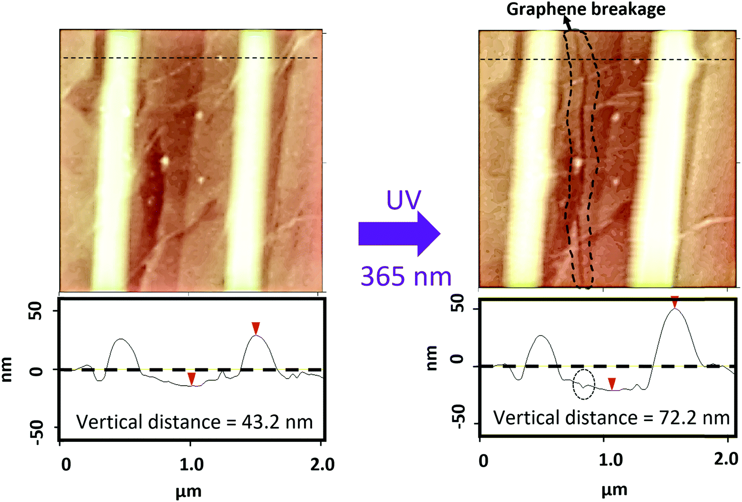 | ||
| Fig. 3 Graphene covered EBL pattern on a DAE single crystal. A large ∼100% height change in the EBL feature displaces the graphene coating and even causes a rupture in the sheet (black dashed outline). | ||
We now turn to the mechanism underlying the photomechanical motion of the EBL features. At the molecular scale, the ring-closing reaction of DAE molecules forms a covalent bond between its two thienyl arms, as illustrated in Fig. 4a. This creates a contraction along the crystal c-axis and expansion along the a-axis. Under UV illumination, the crystal expanded 1.2% along the short axis (a-axis) while no change was detectable along the long axis (b-axis), as shown in ESI,† Fig. S8. The crystal thickness (c-axis) decreased by 2.1% under UV light (ESI,† Fig. S10). The crystals returned back to their original dimensions after visible light irradiation. But these dimensional changes amount to a few percent at most, while the EBL features changed by 30–70%.
 | ||
| Fig. 4 (a) Molecular structure change after the ring-closing photoisomerization leads to compression of the molecule along the c-axis and expanding the molecule along the a-axis. (b–d) AFM images of reversible depth change of the trenches created after sublimation of the EBL features. Colored regions represent cross-sectional areas of the trenches. Pixel counting of the colored areas shows a 25% reversible change during a UV-vis irradiation cycle. | ||
In order to explain the size of this photomechanical effect, we consider the mixed nature of the EBL patterned crystals, consisting of active crystalline regions surrounding the inert amorphous regions. To gain insight into the geometry of the amorphous regions, we developed a strategy to remove them using sublimation. Our hope was that the fragmented DAE molecules in the electron exposed regions would have a lower sublimation temperature than the unexposed DAE crystal, which has a sublimation temperature of 140 °C. Indeed, the exposed areas partially sublimed away at 100 °C, leaving trenches on the crystal surface. The depth of trenches was around 90 nm after heating for 15 min (ESI,† Fig. S12). Further heating did not increase the trench depth. We note that 90 nm is much less than the total thickness (∼2 μm) of the target crystal. From the birefringence measurement, the E-beam exposed area lost crystallinity across the entire thickness. We suspect that the decrease of the electron energy as it penetrated into the crystal resulted in only the top 90 nm of the crystal undergoing extensive fragmentation that allowed it to be sublimed away, while the lower layers experienced heating that led to amorphization but not compete fragmentation.
If we assume that the trenches formed by sublimation represent the volume of deformable solid created by EBL, then we can measure the volume change due to expansion of the surrounding crystal regions. We expect that expansion along the a-axis and compression along the c-axis both affect the volume available to accommodate the inert material. After UV irradiation, we observed a decrease in the vertical trench depth as well as the horizontal cross-section, as shown in Fig. 4b and c. The change could be reversed through 532 nm light irradiation. When the dimensional transformations of the DAE crystal decrease the free volume inside the crystal that can accommodate the inert EBL amorphous region, this amorphous material will be squeezed above the crystal surface. Geometry changes of a 90 nm deep trench before and after UV exposure are shown by the colored areas in Fig. 4b–d. Given the ∼25% decrease in volume shown in Fig. 4b–d, we calculated that it would be sufficient to drive a 22 nm height change, assuming the amorphous solid is squeezed vertically. Visible light converts the DAE back to its open-ring form, and the reverse movement of the crystal lattice restores the free volume, allowing the amorphous solid to retreat back into the crystal. The crystal shape change basically extrudes the amorphous EBL region out of the bulk crystal. Surprisingly, this dynamic extrusion is highly reversible.
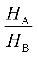
The extrusion mechanism helps explain why the change in trench size (∼25%) is so much larger than the volume change for the entire crystal (∼2%). If we divide the crystal into regions A (intact DAE) and B (inert fragments), we can consider the simple two-dimensional geometry outlined in Fig. 5, where HA/LA and HB/LB are the initial heights/lengths of regions A and B. Photoisomerization drives a dimensional change of region A by a fractional amount of fH and fL along the height and length, respectively. If h and h′ represent the vertical heights of region B above the surface of region A before and after irradiation, we can solve for the ratio h/h′ (ESI,† Fig. S14):
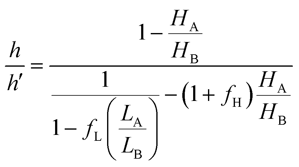 | (1) |
 and
and 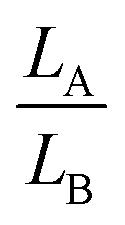 ratios) and the crystal dimensional changes fH and fL. For example, the model predicts that the height ratio
  should decrease for larger HA/HB values (i.e. thicker crystals should have a larger height change, see Table S1 in the ESI,†). Preliminary observations on different DAE crystals are consistent with the predicted trend, although a more systematic study would be needed to confirm this.
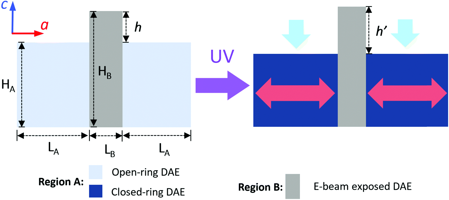 | ||
| Fig. 5 Schematic illustration of the dynamic extrusion mechanism that gives rise to the height change of EBL features under UV irradiation. Expansion along a-axis and shrinkage along c-axis in region A compress the electron beam exposed area B and lead to the increase of feature height from h to h′. | ||
Conclusion
This work has demonstrated the ability of EBL to pattern functional structures into single organic crystals. Nanoscale features written into a photomechanical DAE crystal can be reversibly raised and lowered by alternating UV and visible illumination. The fractional height change of the EBL features ranges from 30–70%, much larger than the changes in overall crystal dimensions. We present evidence for a dynamic extrusion mechanism that enables the dimensional changes of the surrounding crystal to be amplified by the embedded EBL features. This work represents a significant advance in the ability to control molecular crystal morphology and add functionality using lithography methods. Functional optoelectronic devices created by this approach could enable new applications. For example, an array of optically controlled actuators could be used for the reversible localized strain modulation of low dimensional materials to control their electronic and optical properties.43Experimental
Diarylethene crystal growth
The synthesis and crystal structure of 1,2-bis(2-methyl-5-phenyl-3-thienyl)perfluorocyclopentene (DAE) have been described previously.44 To grow plate-like crystals, a DAE powder is first irradiated with 532 nm light to make sure the molecule is in its open-ring form. The powder is then spread onto the bottom of watch glass and heated to 130 °C on a hotplate. A clean glass slide is put on top of the powder at a distance of around 5 mm. The whole setup is covered with aluminum foil to avoid light exposure. Plate-like DAE single crystals with thicknesses of 1–3 μm are formed on the glass slide in 3 hours. Longer deposition times result in thicker and larger crystals.Electron beam lithography on diarylethene single crystals
Glass slides with DAE crystals are coated with 5 nm gold using electron beam evaporation. The gold-coated sample is then mounted in a Leo XB 1540 SEM/FIB system (Zeiss). After the sample is placed in the vacuum SEM chamber, the target crystal is located and aligned with a predesigned pattern using the scanning mode of the SEM. During the imaging step, the electron beam voltage is kept at a low level (5 kV), and the scanning rate is set to the fastest mode to protect the crystal from unnecessary damage. The crystal axis is aligned with the designed pattern by rotating the stage and then selecting a center point on the crystal. Once the aligning step is completed, the lithography program is executed. The electron beam pattering is controlled using NPGS software with a pre-loaded DesignCAD file. The current is set to 200 pA, and the area dosage is set to 4000 C cm−2. After the EBL is finished, the sample is taken out of the chamber and exposed to a KI/I2 solution (Transene Gold Etchant TFA) to remove the gold layer.Graphene transfer on DAE crystals
The transfer of graphene onto DAE crystals is achieved using a method that avoids organic solvents. Monolayer CVD graphene grown on copper (Graphene Supermarket) is first immersed in DI water at 50 °C for 20 hours to detach the graphene sheet from the copper. Then a 5% polyvinyl alcohol aqueous solution was drop cast on the graphene and dried in an oven at 90 °C. A ∼200 μm thick layer of PVA is formed on the graphene. The copper film can then be peeled away using tweezers or a razor blade, leaving the graphene/PVA bilayer. PDMS is then physically attached to the PVA as a supporting layer on the side without graphene. The PDMS/PVA/graphene trilayer is pressed onto a glass substrate covered with DAE single crystals that undergo EBL patterning. The sample is heated at 120 °C for 5 min to make the PVA layer stick to the glass. After the sample is cooled down, the PDMS is peeled off, leaving PVA/graphene on the DAE-covered glass. Finally, the sample is washed in DI water at room temperature for 2 hours to dissolve the PVA, leaving the graphene sheet covering the DAE crystals on top of a glass substrate.Characterization
Atomic force microscopy (AFM) measurements are carried out using a Digital Instruments Nanoscope IIIA scanning probe microscope system (AFM Probe: NSG01, NT-MDT Spectrum Instruments). 365 nm and 532 nm light sources are placed in front of the sample holder to perform in situ illumination. The 365 nm light has an intensity of 0.3 mW mm−2, while the 532 nm light has an intensity of 1.9 mW mm−2, both measured at the sample plane. The UV light was kept on during scans of closed-ring form crystals to maintain the closed form. In order to reverse the reaction and regenerate the open form, one minute of visible light exposure is sufficient. Cross-sectional analysis is conducted on the AFM images using the Nanoscope Control software. Pixel counting of the cross-sectional images is performed in Adobe Photoshop. Optical imaging and birefringence measurements are performed using an Olympus BX51W1 inverted microscope. Raman spectra are collected in Nicolet Almega XR Dispersive Raman microscope using 780 nm laser excitation through a 50× objective (NA = 0.8) with an estimated focus diameter of 1 μm.Conflicts of interest
There are no conflicts to declare.Acknowledgements
This work was supported by the Office of Naval Research through the MURI on Photomechanical Material Systems (ONR N00014-18-1-2624).References
- W. M. Moreau, Semiconductor Lithography: Principles, Practices, and Materials, Plenum Press,New York, 1988 Search PubMed.
- A. L. Briseno, S. C. B. Mannsfeld, M. M. Ling, S. Liu, R. J. Tseng, C. Reese, M. E. Roberts, Y. Yang, F. Wudl and Z. Bao, Patterning organic single-crystal transistor arrays, Nature, 2006, 444, 913–917, DOI:10.1038/nature05427.
- F. S. Wilkinson, R. F. Norwood, J. M. McLellan, L. R. Lawson and D. L. Patrick, Engineered Growth of Organic Crystalline Films Using Liquid Crystal Solvents, J. Am. Chem. Soc., 2006, 128, 16468–16469, DOI:10.1021/ja066153p.
- W. Deng, Y. Lv, X. Zhang, X. Fang, B. Lu, Z. Lu and J. Jie, High-resolution patterning of organic semiconductor single crystal arrays for high-integration organic field-effect transistors, Mater. Today, 2020, 40, 82–90, DOI:10.1016/j.mattod.2020.06.004.
- A. d Campo and E. Arzt, Fabrication Approaches for Generating Complex Micro- and Nanopatterns on Polymeric Surfaces, Chem. Rev., 2008, 108, 911–945, DOI:10.1021/cr050018y.
- Y. Yao, L. Zhang, T. Leydecker and P. Samorì, Direct Photolithography on Molecular Crystals for High Performance Organic Optoelectronic Devices, J. Am. Chem. Soc., 2018, 140, 6984–6990, DOI:10.1021/jacs.8b03526.
- M. S. Alias, Y. Yang, T. K. Ng, I. Dursun, D. Shi, M. I. Saidaminov, D. Priante, O. M. Bakr and B. S. Ooi, Enhanced Etching, Surface Damage Recovery, and Submicron Patterning of Hybrid Perovskites using a Chemically Gas-Assisted Focused-Ion Beam for Subwavelength Grating Photonic Applications, J. Phys. Chem. Lett., 2016, 7, 137–142, DOI:10.1021/acs.jpclett.5b02558.
- W. Li, J. v Baren, A. Berges, E. Bekyarova, C. H. Lui and C. J. Bardeen, Shaping Organic Microcrystals Using Focused Ion Beam Milling, Cryst. Growth Des., 2020, 20, 1583–1589, DOI:10.1021/acs.cgd.9b01327.
- P. H. Schmidt, D. C. Joy, M. L. Kaplan and W. L. Feldmann, Electron beam pattern generation in thin film organic dianhydrides, Appl. Phys. Lett., 1982, 40, 93–95, DOI:10.1063/1.92902.
- L. Mutter, M. Koechlin, M. Jazbinsek and P. Gunter, Direct electron beam writing of channel waveguides in nonlinear optical organic crystals, Opt. Express, 2007, 15, 16828–16838, DOI:10.1364/OE.15.016828.
- L. Persano, A. Camposeo, D. Pisignano, A. Burini, P. Spearman and S. Tavazzi, Electron-Beam Nanopatterning and Spectral Modulation of Organic Molecular Light-Emitting Single Crystals, Langmuir, 2014, 30, 1643–1649, DOI:10.1021/la4033833.
- H. J. Park, M. S. Kim, J. Kim and J. Joo, Fine Control of Photoluminescence and Optical Waveguiding Characteristics of Organic Rubrene Nanorods Using Focused Electron-Beam Irradiation, J. Phys. Chem. C, 2014, 118, 30179–30186, DOI:10.1021/jp508402y.
- W. Tiddi, A. Elsukova, H. T. Le, P. Liu, M. Beleggia and A. Han, Organic Ice Resists, Nano Lett., 2017, 17, 7886–7891, DOI:10.1021/acs.nanolett.7b04190.
- D. Zhao, B. Chang and M. Beleggia, Electron-Beam Patterning of Vapor-Deposited Solid Anisole, ACS Appl. Mater. Interfaces, 2020, 12, 6436–6441, DOI:10.1021/acsami.9b19778.
- Y. Kawata, K. Aoki, Y. Inada, T. Yamao and S. Hotta, Direct fabrication of diffraction grating onto organic single crystals by electron beam lithography, Jpn. J. Appl. Phys., 2018, 57, 03EH11, DOI:10.7567/JJAP.57.03EH11.
- T. H. Borchers, F. Topić, J.-C. Christopherson, O. S. Bushuyev, J. Vainauskas, H. M. Titi, T. Friščić and C. J. Barrett, Cold photo-carving of halogen-bonded co-crystals of a dye and a volatile co-former using visible light, Nat. Chem., 2022, 14, 574–581, DOI:10.1038/s41557-022-00909-0.
- J. M. Abendroth, O. S. Bushuyev, P. S. Weiss and C. J. Barrett, Controlling Motion at the Nanoscale: Rise of the Molecular Machines, ACS Nano, 2015, 9, 7746–7768, DOI:10.1021/acsnano.5b03367.
- P. Naumov, S. Chizhik, M. K. Panda, N. K. Nath and E. Boldyreva, Mechanically Responsive Molecular Crystals, Chem. Rev., 2015, 115, 12440–12490, DOI:10.1021/acs.chemrev.5b00398.
- T. J. White, Photomechanical Materials, Composites, and Systems, Wiley, Hoboken, New Jersey, 1st edn, 2017 Search PubMed.
- H. Koshima, Mechanically Responsive Materials for Soft Robotics, Wiley, Weinheim, Germany, 2020 Search PubMed.
- J. Yoon, P. Bian, J. Kim, T. J. McCarthy and R. C. Hayward, Local Switching of Chemical Patterns through Light-Triggered Unfolding of Creased Hydrogel Surfaces, Angew. Chem., Int. Ed., 2012, 51, 7146–7149, DOI:10.1002/anie.201202692.
- D. Liu, C. W. M. Bastiaansen, J. M. J. D. Toonder and D. J. Broer, Light-Induced Formation of Dynamic and Permanent Surface Topologies in Chiral–Nematic Polymer Networks, Macromolecules, 2012, 45, 8005–8012, DOI:10.1021/ma301628h.
- D. Liu, C. W. M. Bastiaansen, J. M. J. D. Toonder and D. J. Broer, Photo-Switchable Surface Topologies in Chiral Nematic Coatings, Angew. Chem., Int. Ed., 2012, 51, 892–896, DOI:10.1002/anie.201105101.
- K. G. Yager and C. J. Barrett, Photomechanical Surface Patterning in Azo-Polymer Materials, Macromolecules, 2006, 39, 9320–9326, DOI:10.1021/ma061733s.
- M. Saccone, V. Dichiarante, A. Forni, A. Goulet-Hanssens, G. Cavallo, J. Vapaavuori, G. Terraneo, C. J. Barrett, G. Resnati, P. Metrangolo and A. Priimagi, Supramolecular hierarchy among halogen and hydrogen bond donors in light-induced surface patterning, J. Mater. Chem. C, 2015, 3, 759–768, 10.1039/c4tc02315c.
- S.-k Ahn, T. H. Ware, K. M. Lee, V. P. Tondiglia and T. J. White, Photoinduced Topographical Feature Development in Blueprinted Azobenzene-Functionalized Liquid Crystalline Elastomers, Adv. Funct. Mater., 2016, 26, 5819–5826, DOI:10.1002/adfm.201601090.
- Y. S. Zholdassov, D. J. Valles, S. Uddin, J. Korpanty, N. C. Gianneschi and A. B. Braunschweig, Orthogonal Images Concealed Within a Responsive 6-Dimensional Hypersurface, Adv. Mater., 2021, 33, 2100803, DOI:10.1002/adma.202100803.
- A. M. Wong, D. J. Valles, C. Carbonell, C. L. Chambers, A. Y. Rozenfeld, R. W. Aldasooky and A. B. Braunschweig, Controlled-Height Brush Polymer Patterns via Surface-Initiated Thiol-Methacrylate Photopolymerizations, ACS Macro Lett., 2019, 8, 1474–1478, DOI:10.1021/acsmacrolett.9b00699.
- M. Irie, T. Fukaminato, K. Matsuda and S. Kobatake, Photochromism of Diarylethene Molecules and Crystals: Memories, Switches, and Actuators, Chem. Rev., 2014, 114, 12174–12277, DOI:10.1021/cr500249p.
- S. Kobatake, S. Takami, H. Muto, T. Ishikawa and M. Irie, Rapid and reversible shape changes of molecular crystals on photoirradiation, Nature, 2007, 446, 778–781, DOI:10.1038/nature05669.
- F. Terao, M. Morimoto and M. Irie, Light-driven molecular-crystal actuators: rapid and reversible bending of rodlike mixed crystals of diarylethene derivatives, Angew. Chem., Int. Ed., 2012, 51, 901–904, DOI:10.1002/anie.201105585.
- D. Kitagawa and S. Kobatake, Crystal Thickness Dependence of Photoinduced Crystal Bending of 1,2-Bis(2-methyl-5-(4-(1-naphthoyloxymethyl)phenyl)-3-thienyl)perfluorocyclopentene, J. Phys. Chem. C, 2013, 117, 20887–20892, DOI:10.1021/jp4083079.
- D. Kitagawa, H. Nishi and S. Kobatake, Photoinduced twisting of a photochromic diarylethene crystal, Angew. Chem., Int. Ed., 2013, 52, 9320–9322, DOI:10.1002/anie.201304670.
- D. Kitagawa, H. Tsujioka, F. Tong, X. Dong, C. J. Bardeen and S. Kobatake, Control of Photomechanical Crystal Twisting by Illumination Direction, J. Am. Chem. Soc., 2018, 140, 4208–4212, DOI:10.1021/jacs.7b13605.
- M. Morimoto and M. Irie, A diarylethene cocrystal that converts light into mechanical work, J. Am. Chem. Soc., 2010, 132, 14172–14178, DOI:10.1021/ja105356w.
- X. Dong, F. Tong, K. M. Hanson, R. O. Al-Kaysi, D. Kitagawa, S. Kobatake and C. J. Bardeen, Hybrid Organic-Inorganic Photon Powered Actuators Based on Aligned Diaryethene Nanocrystals, Chem. Mater., 2019, 31, 1016–1022, DOI:10.1021/acs.chemmater.8b04568.
- X. Dong, T. Guo, D. Kitagawa, S. Kobatake, P. Palffy-Muhoray and C. J. Bardeen, Effects of Template and Molecular Nanostructure on the Performance of Organic-Inorganic Photomechanical Actuator Membranes, Adv. Funct. Mater., 2019, 1902396, DOI:10.1002/adfm.201902396.
- T. I. Lansakara, F. Tong, C. J. Bardeen and A. V. Tivanski, Mechanical Properties and Photomechanical Fatigue of Macro- and Nanodimensional Diarylethene Molecular Crystals, Nano Lett., 2020, 20, 6744–6749, DOI:10.1021/acs.nanolett.0c02631.
- H. Utsumi, D. Nagahama, H. Nakano and Y. Shirota, A novel family of photochromic amorphous molecular materials based on dithienylethene, J. Mater. Chem., 2000, 10, 2436–2437, 10.1039/B005067I.
- S. Tanaka, M. Toba, T. Nakashima, T. Kawai and K. Yoshino, Photoelectron Spectroscopy Study of Photoresponsive Change in Electronic Structure of Amorphous Photochromic Diarylethene Film, Jpn. J. Appl. Phys., 2008, 47, 1215–1218, DOI:10.1143/JJAP.47.1215.
- S. Kawai, T. Nakashima, Y. Kutsunugi, H. Nakagawa, H. Nakano and T. Kawai, Photochromic amorphous molecular materials based on dibenzothienylthiazole structure, J. Mater. Chem. C, 2009, 19, 3606–3611, 10.1039/B823354C.
- M. Huang, H. Yan, C. Chen, D. Song, T. F. Heinz and J. Hone, Phonon Softening and Crystallographic Orientation of Strained Graphene Studied by Raman Spectroscopy, Proc. Natl. Acad. Sci. U. S. A., 2009, 106, 7304–7308, DOI:10.1073/pnas.0811754106.
- J. M. Kim, M. F. Haque, E. Y. Hsieh, S. M. Nahid, I. Zarin, K.-Y. Jeong, J.-P. So, H.-G. Park and S. Nam, Strain Engineering of Low-Dimensional Materials for Emerging Quantum Phenomena and Functionalities, Adv. Mater., 2022, 2107362, DOI:10.1002/adma.202107362.
- T. Yamada, K. Muto, S. Kobatake and M. Irie, Crystal Structure–Reactivity Correlation in Single-Crystalline Photochromism of 1, 2-Bis(2-methyl-5-phenyl-3-thienyl)perfluorocyclopentene, J. Org. Chem., 2001, 66, 6164–6168, DOI:10.1021/jo010117l.
Footnote |
| † Electronic supplementary information (ESI) available. See DOI: https://doi.org/10.1039/d2nh00205a |
| This journal is © The Royal Society of Chemistry 2022 |