DOI:
10.1039/D0NH00139B
(Communication)
Nanoscale Horiz., 2020,
5, 1088-1095
Reconfigurable all-dielectric Fano metasurfaces for strong full-space intensity modulation of visible light†
Received
3rd March 2020
, Accepted 24th April 2020
First published on 27th April 2020
Abstract
Dynamically reconfigurable nanoscale tuning of visible light properties is one of the ultimate goals both in the academic field of nanophotonics and the optics industry demanding compact and high-resolution display devices. Among various efforts incorporating actively reconfigurable optical materials into metamaterial structures, phase-change materials have been in the spotlight owing to their optical tunability in wide spectral regions including the visible spectrum. However, reconfigurable modulation of visible light intensity has been limited with small modulation depth, reflective schemes, and a lack of profound theoretical background for universal design rules. Here, all-dielectric phase-change Fano metasurface gratings are demonstrated for strong dynamic full-space (reflection and transmission) modulation of visible intensities based on Fano resonances. By judicious periodic couplings between densely arranged meta-atoms containing VO2, phase-change induced thermo-optic modulation of full-space intensities is highly enhanced in the visible spectrum. By providing intuitive design rules, we envision that the proposed study would contribute to nanophotonics-enabled optoelectronics technologies for imaging and sensing.
New concepts
Among various efforts incorporating actively reconfigurable optical materials into metamaterial structures, particularly nanophotonic devices using phase-change materials have been in the spotlight owing to their relatively large optical tunability in wide spectral regions including the visible spectrum. However, in the visible regime, reconfigurable modulation with phase-change materials has been limited with small modulation depth, reflective schemes, and a lack of profound theoretical background for universal design rules. Here, all-dielectric phase-change Fano metasurface gratings are proposed and studied to relieve such conventional drawbacks. We theoretically and experimentally demonstrated strong dynamic full-space (reflection and transmission) modulation of visible intensities based on Fano resonances in all-dielectric metasurface gratings. It is verified that the concept of all-dielectric Fano resonance is highly effective for enhancing phase-change-induced thermo-optic modulation of full-space intensities in the visible spectrum. By providing both intuitive design rules and high performances, we envision that the proposed study would contribute to nanophotonics-enabled optoelectronics technologies for practical imaging and sensing applications.
|
1. Introduction
By the virtue of simple nanofabrication processes and unprecedented optical functionalities within an ultracompact volume, metasurfaces have facilitated the development of a wide range of flat optical applications including displays and sensors.1–5 Their geometric structures are designed in terms of individual subwavelength antennas and their periodic coupling to exhibit the ability of resonant trapping and re-scattering of an incident beam with a desired vectorial wavefront. Ultrathin and functional optical-elements have been demonstrated and studied to effectively replace bulky ray optical elements. By modulating the phase, polarization, and amplitude of reflected or transmitted beams, it has been possible to focus,6 absorb,7 filter,8 and steer9 light with desired properties. These exciting properties of passive functional metasurfaces with fixed optical functions have prompted research on dynamically tunable metasurfaces providing new opportunities, most notably chipscale beam steering devices and ultrathin modulators. Actively tunable material platforms including graphene,10–12 semiconductors,13–15 transparent conducting oxides,16–18 liquid crystals,19 phase-change materials (PCM),20–31 and mechanical actuators32–34 have been extensively studied in the last decade. However, due to the extremely short interaction length for light–matter interactions in resonant metasurfaces, all of these platforms lack good performances of practical value. Thus, it is hard to achieve large tunability, high efficiency, and modulation capability in multiple optical properties using a single resonant metadevice. In particular, modulation of visible light waves in free space has been hardly achieved despite its substantial practical value in miniaturized display and sensing technologies with extremely high resolution. Rather than the other materials and platforms mentioned above, PCMs such as vanadium dioxide (VO2) and chalcogenide compounds show large thermo-optic tunability of the dielectric functions in the visible and near-infrared regime.20–31 PCM-based metadevices provide a large design degree of freedom in the optical regime by virtue of their relatively large tunability of the dielectric function compared to other material platforms. Several experimental studies have reported modulation of optical intensities using PCMs in the optical range. Compared to the near and mid infrared range, nanophotonic designs of visible range metadevices based on PCMs are very challenging since they show relatively small tunability and large absorption coefficients with low quality factors at visible wavelengths. The empirical demonstration of large intensity modulation based on a strong physical background and intuition has been elusive. Moreover, despite the clear significance and necessity of extremely miniaturized and integrated flat optics systems, dynamic and effective full-space modulation of both reflection and transmission beams has never been studied thoroughly except for several passive metasurfaces.35,36
In this paper, we propose a holistic study on simple and effective Fano-resonance methods to tune full-space visible wave intensities using all-dielectric phase-change metasurface gratings based on VO2 phase-change. Via theoretical and experimental studies, we show that judicious combinations of Fano resonance phenomena in metasurface gratings and the insulator-to-metal transition (IMT) of a VO2 film exhibit good modulation performances in simple structures in the visible range. Here, a framework of optical Fano resonance, one of the general phenomena in nanophotonic systems, is introduced for systematic and intuitive understanding.37–44 For rigorous theoretical design and analysis, zeroth and second-order effective medium theory (EMT), temporal coupled mode theory (TCMT) and Rayleigh–Wood's anomaly (RWA) are introduced in three different types of metasurface devices. The rest of the paper is as follows. Firstly, the thermo-optic properties of a VO2 film, VO2 nano-waveguide modes, and resonators are investigated as a fundamental step of the study. Then, nanostructured VO2 metafilms and diffractive silicon–VO2 hybrid metagratings are demonstrated with different dynamic modulation characteristics. Last, concluding remarks are made with future perspectives.
2. Results and discussion
2.1 Thermo-optic properties of VO2 waveguides and resonators
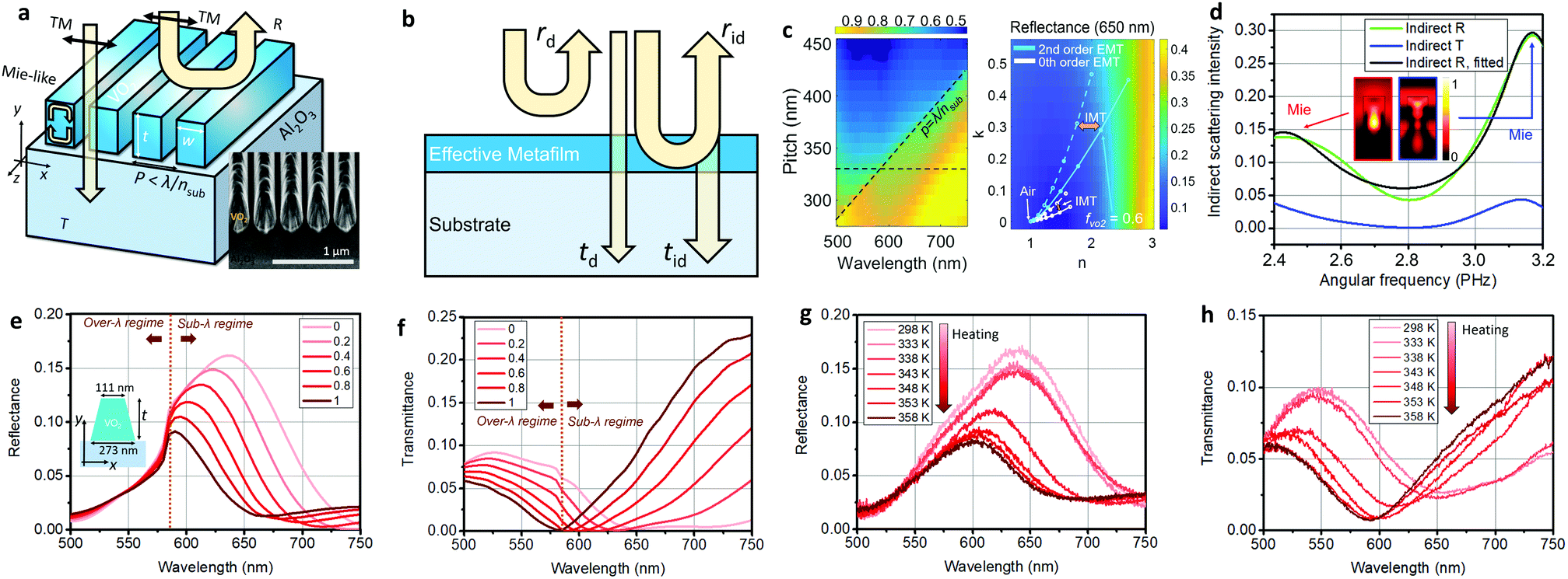
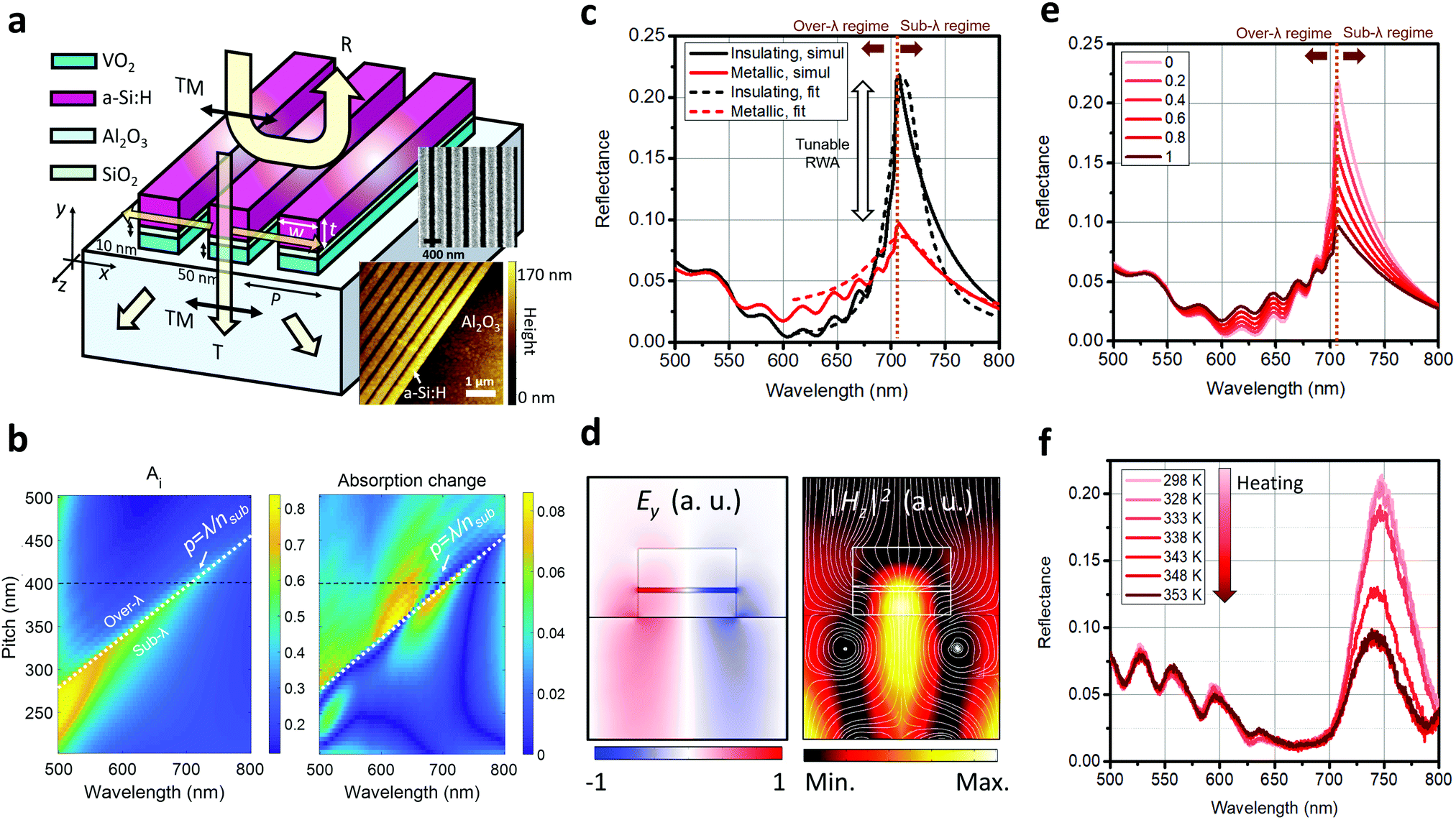
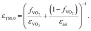
Ahead of reconfigurable metadevice design, we characterized a tunable VO2 thin film made by conventional pulsed laser deposition on a sapphire substrate45,46 (see part 1 of the ESI†). The dielectric function implies that VO2 is a highly absorptive dielectric in the visible range and it shows a decrease and increase of its refractive index in heating and cooling processes. Based on such tunable VO2 properties and low loss materials47 (see part 2 of the ESI† for the optical properties of a-Si:H), the design strategy is focused on incorporating this thin film into all-dielectric Fano metasurfaces for simultaneous effective control of reflection, absorption, and transmission as shown in Fig. 1(a). In general, an optical Fano resonance with an asymmetric spectral lineshape is constructed by coherent interference of bright continuum scattering and resonant dark mode scattering.37,39 Thus, individual VO2-containing meta-atoms and their periodic coupling effects are considered rigorously to design tunable and strong Fano interference. As depicted in the inset figures of Fig. 1(a), nano-resonators with Mie resonances48 and gap photonic mode resonances (GPMR),49 which confine light mostly in the VO2 and lossless low-index SiO2 regions, respectively, are considered as unit cell meta-atoms. The first one inherits the conventional advantages of strong magnetic Mie resonances owing to the relatively large refractive index of VO2 so that light–VO2 interactions are enhanced easily. On the other hand, a novel GPMR meta-atom shows more advantages with respect to signal efficiency and quality factor as the field penetration into an active VO2 region is lowered compared to the Mie type meta-atom. The GPMR meta-atom shows interesting field-confining features resembling gap plasmon resonances50 which exhibit plasmon-assisted utlracompact capacitive field confinement. However, as a-Si:H and SiO2 show low absorption loss in the visible regime, GPMR is more advantageous for modulating both reflection and transmission beams rather than gap plasmon resonances. Fig. 1(b) shows an analytical comparison of the effective quality factors and tunability of the refractive index in a homogeneous VO2 medium, 100 nm-thick VO2 waveguide, and hybrid a-Si:H (50 nm-thick)–SiO2 (10 nm-thick)–VO2 (50 nm-thick) waveguide at room temperature. Numerical full-field simulations are conducted using the RF solver of COMSOL Multiphysics 5.3 and custom-built rigorous coupled wave analysis. The solid, dashed, and short dashed lines refer to the homogeneous VO2, VO2 waveguide, and hybrid a-Si:H–SiO2–VO2 waveguide, respectively. It is clearly shown that the intrinsic material quality factor, Q = |ε1/ε2|, of about 3 is too low to make a strong resonance in the bare film. Here, ε1 and ε2 are the real and imaginary parts of the dielectric function, respectively. On the other hand, the nanostructured waveguides show improved effective quality factor (Qeff = |ε1,eff/ε2,eff|) according to their geometry and wavelength, as described in Fig. 1(b). The effective guided mode index, neff, is the square root of ε1,eff + iε2,eff. By sacrificing a bit of effective mode index tunability, it is expected that a more efficient and narrower resonance design could be achieved based on the waveguide study. In Fig. 1(c) and (d), Mie-like resonances and GPMR are numerically investigated with good tunability and enhanced resonance strength compared to the bare film. The two sub-figures in Fig. 1(c) show two strong absorption resonances in a 2-dimensional VO2 nanobeam resonator. The sub-figures in Fig. 1(d) describe the electromagnetic field properties at the GPMR with enhanced Q-factor compared to the Mie-like one (Fig. 1(c)). Based on the two distinct resonance properties, tunable Fano metasurface gratings are demonstrated with judicious periodic arrangements of the reconfigurable meta-atoms for modulation of reflection and transmission. A 1-dimensional grating structure is advantageous to study fundamental physical principles of reconfigurable Fano resonances and to apply electrodes for electrical heating without harm to designed optical functions,14,16–18 rather than 2-dimensionally patterned metasurfaces.
 |
| | Fig. 1 (a) Concepts of full-space modulation by a reconfigurable all-dielectric Fano metasurface designed using efficient meta-atoms and their periodic coupling. rd, rid, td, and tid correspond to direct reflection, indirect reflection, direct transmission, and indirect transmission coefficients, respectively. (b) Comparison of the calculated waveguide effect in terms of the effective quality factor in the insulating phase (left y-axis, black lines) and effective mode index change (right y axis, blue lines). Solid, dashed, and dotted lines denote a homogeneous VO2 medium, 100 nm-thick VO2 slab waveguide, and hybrid a-Si:H–SiO2–VO2 waveguide, respectively. The inset field profiles show the normalized Ey field of the guided TM-polarized modes in the VO2 slab waveguide and the hybrid waveguide in the insulating phase (wavelength: 600 nm). (c) VO2 phase-change-induced absorption modulation of the VO2 ridge resonator (width = 100 nm, thickness = 320 nm). The sub-figures denote the normalized magnetic field intensity at the resonance peaks excited by TM-polarized normal incidence from the top. The white stream lines in the sub-figures present the power flow of incident TM illumination around the resonator. (d) VO2 phase-change-induced absorption modulation of the hybrid silicon–silicon dioxide–VO2 resonator. The resonator width, a-Si:H thickness, SiO2 thickness, and VO2 thickness are 200 nm, 50 nm, 10 nm, and 50 nm, respectively. The subplots show the normalized real part of the Ey field (left) and magnetic field intensity (right) at the insulating phase resonance (wavelength: 600 nm) under TM illumination. | |
2.2 Fano-resonant modulation of a VO2 metafilm
We first propose a nanostructured metafilm modulator made of periodic subwavelength VO2 nanobeams. The metafilm strategy has been widely studied for various nanoscale optoelectronics and photonics applications51–54 in terms of Mie resonances and their periodic coupling effect owing to its simple but extraordinary properties of light trapping and modulation with large design extensibility. Since VO2 shows significantly tunable dielectric properties in the visible range, densely arranged subwavelength VO2 nanobeams can be of great advantage to generate strongly reconfigurable Fano resonances with large absorption. As depicted in Fig. 2(a), we propose a Fano-resonant phase-change VO2 metafilm excited by normal illumination with transverse magnetic (TM) polarization for a dielectric magnetic-like Mie resonance. We fix the thickness (tVO2) of the VO2 at 320 nm and the width of each VO2 nanobeam (w) at 180 nm considering fabrication stability of pulsed laser deposition (VO2 deposition) and focused ion beam milling (nano-patterning). The inset figure in Fig. 2(a) shows a well-defined fabricated metafilm cross-section image captured by scanning electron microscopy assisted by focused ion beam milling (see the detailed fabrication process in part 3 of the ESI†). The working principle of the resonant metafilm device can be described as an effective tunable metafilm with direct and indirect resonant scattering for two radiation channels (Fig. 2(b)). The effective metafilm is constructed from a composite of air and VO2 nanobeams. The design and analysis of the device are conducted based on the 0th and 2nd order EMTs55,56 and TCMT formalism38–42 as follows. As shown in the left 2-dimensional plot of Fig. 2(c), when t and w are fixed, variation of the unit cell pitch (p) critically affects the optical resonance spectra as the filling factor (fVO2 = w/p) of VO2 in the metafilm layer and its effective refractive index (εTM and εTE) change. Such effective medium analysis of the metafilm can be further studied via the 0th and 2nd order effective medium theories. According to the 0th order EMT of such a 2-dimensional periodic nanobeam structure,55 the effective dielectric functions for TE and TM polarizations are described as follows.| | | εTE,0 = fVO2εVO2 + (1 − fVO2)εair, | (1) |
| |  | (2) |
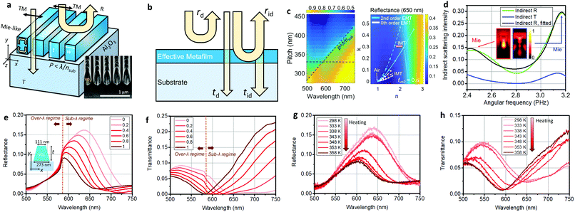 |
| | Fig. 2 (a) Schematic diagram of the nanostructured VO2 metafilm (t = 320 nm and w = 180 nm). The subplot shows a scanning electron micrograph of the fabricated device (b) Schematic diagram of the two-port Fano-resonance mechanism in the metafilm assisted by effective medium theory. rd, rid, td, and tid correspond to the direct reflection, indirect reflection, direct transmission, and indirect transmission coefficients, respectively. (c) Design of the dynamically tunable metafilm. The left 2-dimensional plot shows the absorptance spectra according to varying pitch (p) of the unit cell. The oblique and horizontal black dashed lines refer to the diffraction phase-matching condition and p = 330 nm condition, respectively. The right figure shows the reflectance of the approximated metafilm (thickness = 320 nm) effective medium depicted in (b) according to varying refractive index and extinction coefficient at a wavelength of 650 nm. The white and sky blue coloured lines denote the 1st and 2nd order effective medium theory for TM polarization as the filling factor of VO2 (fVO2) varies from 0 to 0.7. The solid and dashed lines exhibit the location of the effective index coordinate in the insulating and metallic phases of VO2, respectively. (d) Indirect scattering intensity of transmission and reflection. The bright green, blue, and black legends refer to indirect reflectance, indirect transmittance, and doubly resonant Lorentzian fitting results of indirect reflectance. The sub-figures show the two indirect resonances via normalized magnetic field intensity profiles. The full-field simulation results of gradually tunable (e) reflectance and (f) transmittance spectra according to the filling factor (legends) of the metallic phase VO2. The simulations are conducted for the tapered metafilm (inset figure of (e)). Measurement results of gradually tunable (g) reflectance and (h) transmittance spectra in the heating process. The legends in (e) and (f) denote the filling factors of metallic VO2, and thus the 0 and 1 values correspond to the insulating and metallic phases, respectively. The legends in (g) and (h) denote device temperatures in the heating process. | |
However, it is well known that the 2nd order EMT is much more accurate than the 0th order one when the pitch of the unit cell is not much smaller than the wavelength, as is the case with photonic crystals and general metasurfaces exhibiting Fano resonances.51–56
| |  | (3) |
As shown in
eqn (3), the second order EMT for TM polarization is determined by adding an additional 2nd order compensation term proportional to (
p/
λ)
2 based on the 0th order formulas in
eqn (1) and (2). We analytically calculated the reflectance resonance of the effective metafilm at a wavelength of 650 nm using Airy's formula for various effective complex refractive indices of the metafilm. The two distinct 0th and 2nd order EMT calculation curves in the 2-dimensional reflectance map show that the 2nd order curves accurately account for the reflectance at the wavelength of 650 nm both in the insulating and metallic phases of VO
2 in comparison to the full-field simulation results. While the 2nd order EMT is useful to estimate effective metafilm characteristic more accurately, the 0th order EMT is highly advantageous to explain the Fano resonance mechanism. The reflection and transmission beams are generated by interference between the direct background scattering (bright mode) and indirect resonant scattering (dark mode) of the metafilm.
37–44 Since the 0th order EMT is based on the assumption of the deep subwavelength limit and it cannot explain subwavelength Mie or plasmonic resonances in metamaterials,
rd and
td are the reflection and transmission coefficients of the thin metafilm with dielectric functions of the 0th order EMT. On the other hand,
rid and
tid originate from local subwavelength optical resonances with Lorentzian characteristics. Thus, using temporal coupled mode theory with the 0th order EMT, two port radiation (reflection and transmission) of a single Fano resonance mode can be modelled analytically as follows (part 4 of the ESI
†).
38–42| |  | (4) |
| |  | (5) |
| |  | (6) |
rtot,
ttot,
rd,
rid,
td, and
tid in the above equations are the complex coefficients of total reflection, total transmission, direct reflection, indirect reflection, direct transmission, and indirect transmission, respectively. It is known that direct scatterings
rd and
td are analytically calculated as Fabry–Pérot scatterings of reflection and transmission of a dielectric film with a dielectric function of the zeroth order EMT in
eqn (2). Then, the
rid and
tid indirect resonant pathways account for Lorentzian type optical resonance in the system. Thus, we conducted numerical fitting of indirect scattering intensities |
rid|
2 and |
tid|
2 by determining
a,
b,
ω0, and
γtot (part 5 of the ESI
†). However, the formulation of TCMT does not perfectly account for the low
Q-factor resonance and multi-resonant case.
41 As depicted in
Fig. 2(d), dual indirect resonances are observed in the subwavelength regime. The inset figures of the magnetic field intensity profiles show two resonances with large field enhancement inside the VO
2 nanobeams. We conducted numerical fitting in the insulating phase based on an approximated single resonance formulation near the resonances. By approximately fitting two different Lorentzian resonances independently and adding them, the full spectrum of the reflection is fitted. It is also worth noting that the |
tid|
2 spectrum is very similar to |
rid|
2 in terms of the resonance location, which matches well with the TCMT formulation (see part 5 of the ESI
† for detailed fitting results).
The simulation results considering the fabricated device with tapering walls in Fig. 2(e) and (f) exhibit gradually tunable reflection and transmission via the phase change of VO2 similar to the non-tapered ideal design (part 6 of the ESI†). The gradual phase change is analytically approximated as the Maxwell-Garnett EMT for intermediate phases between the insulating and metallic phases (part 7 of the ESI†). The measurement results in the heating process in Fig. 2(g) and (h) also match well with the simulation results (see part 8 of the ESI† for reconfigurable and repetitive thermo-optic measurement results). It is remarkable that a large modulation depth reaching 0.8 in a broad bandwidth is achieved both in the visible reflection and transmission intensities (part 8 of the ESI†). Here, the modulation depth (η) is defined as η = |Ii − Im|/max(Ii,Im), which is a positive value between 0 and 1. Ii and Im denote the signal intensities in the insulating and metallic phases, respectively.
2.3 Fano-resonant modulation of a VO2 metafilm with a transparent dielectric coating
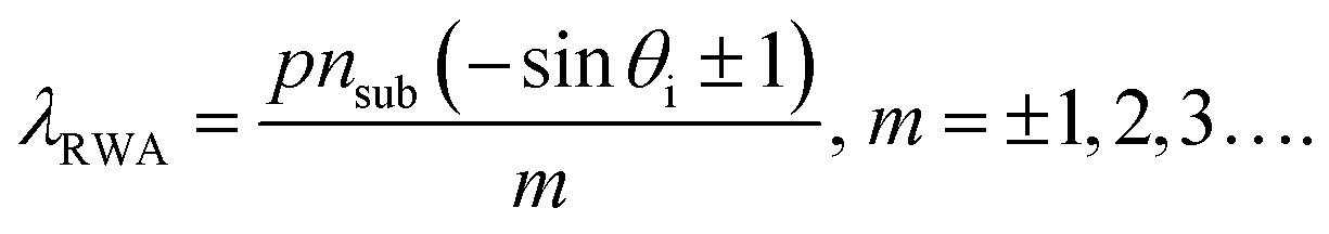
In the previous section, it is verified that nano-structuring of a VO2 thick film as a nanobeam type metafilm is simple and effective to modulate full-space visible intensities. In this section, we propose a simple additional method of a transparent optical coating on the metafilm to improve the Q-factor (spectral bandwidth) and to make use of a different Fano-resonance mechanism, RWA, in addition to coupled Mie resonance. By spin-coating a transparent optical film (hydrogen silsesquioxane, HSQ, with a refractive index of 1.41) on the VO2 metafilm device, an additional sharp Fano resonance is generated and the tunability of the coupled Mie resonance can be enhanced. Fig. 3(a) shows a schematic illustration of the transparent dielectric-coated metafilm device, and the inset figure shows the fabricated device image captured by a scanning electron micrograph (see the detailed fabrication process in part 3 of the ESI†). A full-field simulation is conducted to investigate the effect of the HSQ spin coating thickness on the absorption resonance spectra (Fig. 3(b)). Here, Δt is the difference between the HSQ thickness (thsq) and VO2 thickness (t = 320 nm). As shown in the plots of Fig. 3(b), two absorption resonances are generated. One is the strong near-unity absorption resonance with coupled Mie scatterings excited near the wavelength of the RWA condition of phase-matching as described in eqn (7).57–61| |  | (7) |
Here, nsub and θi are the refractive index of the substrate (sapphire) and the incident illumination angle. In addition another Mie resonance is generated with relatively weak resonance strength in the red–near infrared wavelength region. In the case of the weaker one, EMT is an effective way to analyse the resonance (Fig. 3(c)). The 2nd order EMT accurately accounts for sub-wavelength range resonance switching of reflectance compared to the 0th order EMT. The inset figure of Fig. 3(c) of the HSQ coated metafilm describes the reflectance calculation scheme using EMT. The 320 nm-thick metafilm layer made of VO2 nanobeams and HSQ nanobeams is capped between the 80 nm-thick HSQ coating and half-infinite sapphire substrate, and the effective dielectric function of the metafilm layer is described by EMT.
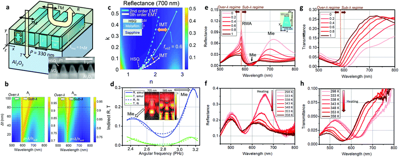 |
| | Fig. 3 (a) Schematic diagram of the transparent dielectric-covered VO2 metafilm (p = 330 nm, t = 320 nm, and w = 180 nm). The subplot shows a cross-sectional scanning electron micrograph of the fabricated device. (b) Design of the dynamically tunable metafilm. The 2-dimensional plots show the absorptance spectra according to varying pitch (p) of the unit cell in the insulating (left) and metallic (right) phases, respectively. The horizontal black dashed and vertical white dashed lines refer to the selected HSQ deposition condition (thsq = t + 80 nm) and diffraction phase-matching condition, respectively. (c) Reflectance map of the approximated metafilm (thickness = 320 nm) effective medium according to varying refractive index and extinction coefficient at a wavelength of 700 nm. The white and sky blue coloured lines denote the 1st and 2nd order effective medium theory for TM polarization as the filling factor of VO2 (fVO2) varies from 0 to 0.7. The solid and dashed lines exhibit the location of the effective index coordinate in the insulating and metallic phases of VO2, respectively. (d) Indirect scattering intensity of transmission and reflection. The bright green and blue legends refer to indirect transmittance and indirect reflectance, respectively. The doubly resonant Lorentzian fitting results of indirect scatterings correspond to the dashed lines. The subplots of (d) show the resonant magnetic field intensity profiles in the insulating phase at a wavelength of 585 nm (left) and 705 nm (right) normalized equally. Phase-change induced gradually tunable reflectance spectra from (e) simulations and (f) measurements. The inset figure of (e) describes the simulation unit cell considering tapering walls. Phase-change induced gradually tunable transmittance spectra from (g) simulations and (h) measurements. The experimental results of (f) reflectance and (h) transmittance spectra are measured in the heating process. The legends in (e) and (g) denote the filling factors of metallic VO2, and thus the 0 and 1 values correspond to the insulating and metallic phases, respectively. The legends in (f) and (h) denote device temperatures in the heating process. | |
As discussed in the previous section, the 0th order EMT explains direct scatterings while indirect scatterings can be modelled via Lorentzian resonance. The plots in Fig. 3(d) show dual resonances of indirect reflection and transmission Lorentzian resonance (see detailed fitting results in part 9 of the ESI†). The inset figures of the magnetic field intensity show that two Lorentzian resonances are excited as coupled Mie-like resonances with large field enhancement and different field profiles. The resonance at higher frequencies shows higher coupling between neighbouring meta-atoms, while the other one shows higher confinement only in the VO2 region rather than the HSQ region. This abrupt evanescent coupling induced RWA resonance occurs since the metafilm layer is composed of HSQ (refractive index of about 1.41) and VO2 so that the index contrast is lowered and the nearest-neighbour coupling effect of meta-atoms is increased compared to the air–VO2 composite metafilm.57–61 As the indirect absorption resonance at higher frequency is well overlapped with the RWA wavelength in the spectrum, a strong RWA resonance is formed. Such two different resonances contribute to large tunability in reflectance and transmittance (Fig. 3(e)–(h)). Fig. 3(e) and (f) show the reflectance tuning results of numerical calculations and measurements, respectively. Fig. 3(g) and (h) present the transmittance results of simulations and measurements, respectively. While the reflectance and transmittance resonances show blue and red shifts on heating and cooling of the device, the Mie resonance anti-reflection effect, RWA, and Mie resonances are tuned with large modulation depths reaching about 0.8 and 1 (see Fig. 3(e)–(h) and part 10 of the ESI†). The difference between the calculation and the experiment seen in Fig. 3(e) and (f) mainly originates from the inherent angle sensitivity of the sharp RWA resonance. It is numerically found that portions of slightly oblique incidence light due to the highly focusing objective lens (50×) in the microscopy setup critically suppress the sharp RWA resonance and induce the blue shifted resonance with a lowered Q-factor (see the detailed numerical analysis in parts 11 and 12 of the ESI†).57–61
2.4 Fano-resonant Rayleigh–Wood's anomaly in a hybrid metagrating
In this section, we propose a Fano-resonant diffractive metagrating for enhanced Q-factor and efficiency. Since it is hard to make a high Q-factor even with conventional low loss dielectric metasurfaces and nanoantennas, achieving a high Q-factor with high signal efficiency and its reconfigurable modulation in lossy PCM metasurfaces is limited with conventional dielectric resonances including the Mie resonant VO2 metafilms proposed in the previous section.
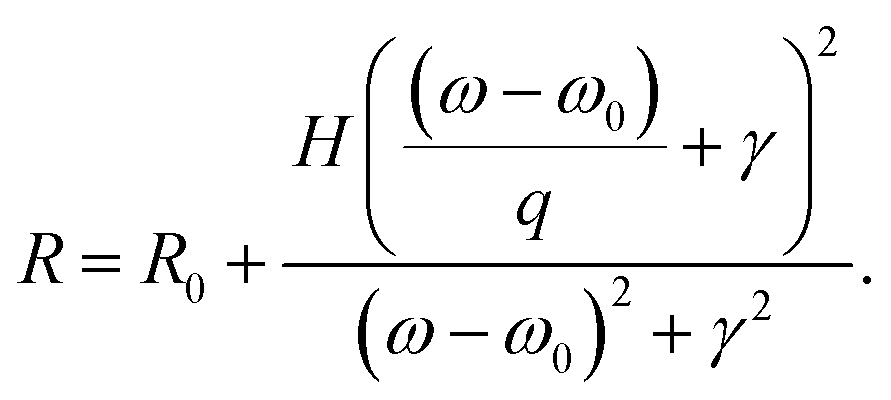
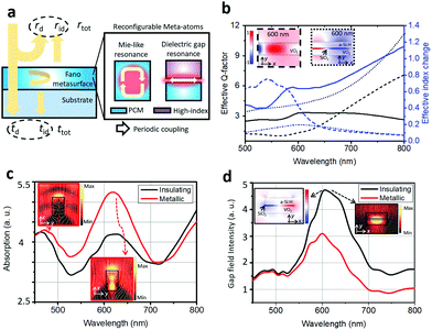
Our idea to relieve these limitations is to combine the less lossy GPMR meta-atom (Fig. 1(a) and (d)) and RWA resonance phenomenon at the RWA diffraction condition (p = λ/nsub). Fig. 4(a) describes a schematic diagram of the metagrating device. The two inset figures of the scanning electron micrograph (upper) and atomic force micrograph (lower) of the top-view image show a fabricated metagrating with a 400 nm pitch produced by the conventional e-beam lithography technique using a thin sputtered VO2 thin film (see the details in part 13 and 14 of the ESI†). In a diffractive regime (p < λ/nsub), as discussed in the previous section, the 1st and −1st diffraction channels are generated and RWA occurs with extraordinary resonance effects leading to sharp spectral change, which can be engineered by designing individual unit cell nanostructures.57–61 In this case, to enhance the Q-factor, the low loss GPMR meta-atom is adopted. It is expected that the phase-change of VO2 would only affect the strength of the sharp resonance peak at the RWA wavelength (λRWA) but not the location of the resonance wavelength according to eqn (7). To investigate the principles of the hybrid metagrating, we calculated absorption spectra according to varying pitch length in the insulating phase as shown in Fig. 4(b) (left). With the fixed geometry of the unit cell structure, the pitch is chosen to be 400 nm for achieving a sharp resonance with large tunability within the visible regime (black dashed lines in Fig. 4(b)). With such an abrupt sharp absorption resonance peak, the reflectance peak is significantly modulated with a narrow and asymmetric Fano lineshape near resonance (Fig. 4(c)).57–61 The numerically calculated and measured reflectance spectra in both VO2 phases are successfully fitted to the conventional Fano resonance formula (Fig. 4(c) and part 15 of the ESI†),37
| | 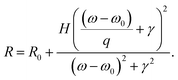 | (8) |
Here,
R,
R0, H,
q,
γ,
ω, and
ω0 refer to the reflectance, baseline reflectance, resonance strength, asymmetry factor, decay rate, angular frequency, and resonant angular frequency, respectively. The electromagnetic field profiles in
Fig. 4(d) at the resonance show that the GPMR phenomenon with large field confinement occurs and a large amount of absorption is generated at the VO
2 region rather than the SiO
2 and a-Si:H regions. Gradual full-space modulation performances with enhanced
Q-factor and efficiency are verified both in simulations (
Fig. 4(e)) and measurements (
Fig. 4(f)). Moreover, the transmittance dip can be modulated significantly near the RWA resonance (part 16 of the ESI
†). Similar to the case in the previous section, the little discrepancy between the calculations and experiments seen in
Fig. 4(e) and (f) mainly originates from the angle sensitivity of the sharp RWA resonance. Owing to portions of oblique incidence light due to the focusing objective lens (10×) in the microscopy setup (part 12 of the ESI
†), the
Q-factor and resonance location of the RWA resonance are a little distorted (see the detailed numerical discussions in part 17 of the ESI
†).
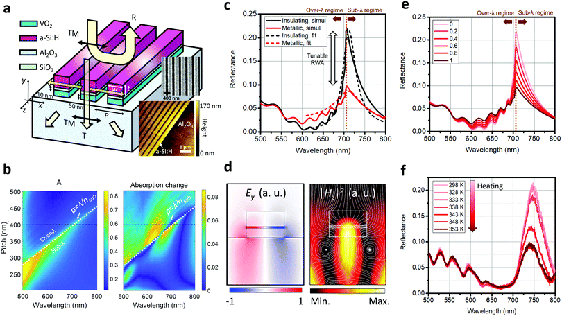 |
| | Fig. 4 (a) Schematic diagram of the hybrid metagrating (t = 80 nm and w = 200 nm). The subplots show top-view images of the scanning electron micrograph (up) and atomic force micrograph (down) of the fabricated device with a pitch of 400 nm. (b) Investigation of the pitch effect on the dynamically tunable metagrating. The 2-dimensional plots show the insulating phase absorptance (left) and phase-change-induced absolute difference of absorptance spectra (right) according to the varying pitch of the unit cell. The horizontal black dashed and oblique white dashed lines refer to the selected pitch condition (p = 400 nm) and diffraction phase-matching condition, respectively. (c) Numerically calculated reflectance spectra in the insulating and metallic phases (solid lines) with Fano-resonance fitting results (dashed lines) (d) Normalized profiles of the Ey field (left) and magnetic field intensity (right) at the insulating phase resonance. The white streamlines in the left sub-figure denote the power flow of TM-polarized incident light toward the resonator. (e) Simulation and (f) measurement results of reflectance. The legends in (e) denote the filling factors of metallic VO2, and thus the 0 and 1 values correspond to the insulating and metallic phases, respectively. The legends in (f) denote the device temperature in the heating process. | |
3. Conclusions
In conclusion, inspired by Fano resonances with EMT and RWA in periodic nanophotonic gratings, we demonstrated simple and effective metasurface devices to dynamically modulate the visible light intensity in both reflection and transmission beams for the first time. We proposed and studied three different types of Fano-resonant grating devices with different modulation characteristics. By simultaneously achieving high modulation depths of both reflection and transmission, we expect that the proposed methods of all dielectric Fano-resonant dynamic light modulation could be applied for practical use in a wide range of optoelectronics technologies such as advanced high-resolution spatial light modulators, structural colours, smart windows, photodetectors, tunable anti-reflection coatings, tunable smart windows, thermal light sources, and image sensors that essentially require strong and efficient visible range operation. Moreover, the universal intuitive design rules provided in this paper would be also fruitful to design reconfigurable nanophotonic devices based on other active material platforms. It seems to be very promising that a spatial light modulator with the proposed metasurface grating pixels can be also demonstrated with pixel-by-pixel electro-thermal control if transparent conductors like indium tin oxide and graphene are introduced for electrical heating.
Conflicts of interest
There are no conflicts to declare.
Acknowledgements
This research was supported by the National Research Foundation of Korea (NRF) funded by the Ministry of Science and ICT (2020R1A2B5B02002730) and the BK21 Plus Project in 2020 (21A20131612805). The authors thank Dr Sang-Eun Mun for fruitful discussions. I. K. and J. R. acknowledge the Global PhD fellowship (NRF-2016H1A2A1906519) and a NRF grant (CAMM-2019M3A6B3030637), respectively funded by NRF-MSIT of the Korean government. H. Y. and J. S. acknowledge the support from the Basic Science Research Program through the National Research Foundation of Korea (NRF) funded by the Ministry of Science and ICT (2020R1A2C2006389). Parts of this study have been performed using facilities at the IBS Center for Correlated Electron Systems, Seoul National University and Electronics and Telecommunications Research Institute.
References
- N. Yu and F. Capasso, Nat. Mater., 2014, 13, 139–150 CrossRef CAS.
- N. I. Zheludev and Y. S. Kivshar, Nat. Mater., 2012, 11, 917–924 CrossRef CAS.
- Y. Lee, S.-J. Kim, H. Park and B. Lee, Sensors, 2017, 17, 1726 CrossRef.
- P. Genevet and F. Capasso, Rep. Prog. Phys., 2015, 78, 024401 CrossRef.
- X. Luo, D. Tsai, M. Gu and M. Hong, Chem. Soc. Rev., 2019, 48, 2458–2494 RSC.
- M. Khorasaninejad, W. T. Chen, R. C. Devlin, J. Oh, A. Y. Zhu and F. Capasso, Science, 2016, 352, 1190–1194 CrossRef CAS PubMed.
- M. A. Kats and F. Capasso, Laser Photonics Rev., 2016, 10, 735–749 CrossRef CAS.
- N. Yu, F. Aieta, P. Genevet, M. A. Kats, Z. Gaburro and F. Capasso, Nano Lett., 2012, 12, 6328–6333 CrossRef CAS.
- N. Yu, P. Genevet, M. A. Kats, F. Aieta, J. P. Tetienne, F. Capasso and Z. Gaburro, Science, 2011, 334, 333–337 CrossRef CAS.
- Y. Yao, M. A. Kats, P. Genevet, N. Yu, Y. Song, J. Kong and F. Capasso, Nano Lett., 2013, 13, 1257–1264 CrossRef CAS.
- V. W. Brar, M. S. Jang, M. Sherrott, J. J. Lopez and H. A. Atwater, Nano Lett., 2013, 13, 2541–2547 CrossRef CAS.
- S. Kim, M. S. Jang, V. W. Brar, K. W. Mauser, L. Kim and H. A. Atwater, Nano Lett., 2018, 18, 971–979 CrossRef CAS PubMed.
- P. P. Iyer, N. A. Butakov and J. A. Schuller, ACS Photonics, 2015, 2, 1077–1084 CrossRef CAS.
- Y. Horie, A. Arbabi, E. Arbabi, S. M. Kamali and A. Faraon, ACS Photonics, 2017, 5, 1711–1717 CrossRef.
- T. Lewi, P. P. Iyer, N. A. Butakov, A. A. Mikhailovsky and J. A. Schuller, Nano Lett., 2015, 15, 8188–8193 CrossRef CAS PubMed.
- J. Park, J. H. Kang, X. Liu and M. L. Brongersma, Sci. Rep., 2015, 5, 15754 CrossRef CAS PubMed.
- Y.-Y. Huang, H. W. Lee, R. Sokhoyan, R. A. Pala, K. Thyagarajan, S. Han, D. P. Tsai and H. A. Atwater, Nano Lett., 2016, 16, 5319–5325 CrossRef CAS.
- G. K. Shirmanesh, R. Sokhoyan, R. A. Pala and H. A. Atwater, Nano Lett., 2018, 18, 2957–2963 CrossRef.
- S. Q. Li, X. Xu, R. M. Veetil, V. Valuckas, R. P. Domínguez and A. I. Kuznetsov, Science, 2019, 364, 1087–1090 CrossRef CAS.
- M. J. Dicken, K. Aydin, I. M. Pryce, L. A. Sweatlock, E. M. Boyd, S. Walavalkar, J. Ma and H. A. Atwater, Opt. Express, 2009, 17, 20975–20990 CrossRef.
- S.-J. Kim, H. Yun, K. Park, J. Hong, J.-G. Yun, K. Lee, J. Kim, S. J. Jeong, S.-E. Mun, J. Sung, Y. W. Lee and B. Lee, Sci. Rep., 2017, 7, 43723 CrossRef.
- M. Seo, J. Kyoung, H. Park, S. Koo, H. S. Kim, H. Bernien, B. J. Kim, J. H. Choe, Y. H. Ahn, H.-T. Kim, N. Park, Q.-H. Park, K. Ahn and D.-S. Kim, Nano Lett., 2010, 10, 2064–2068 CrossRef CAS.
- S.-J. Kim, S. Choi, C. Choi, Y. Lee, J. Sung, H. Yun, J. Jeong, S.-E. Mun, Y. W. Lee and B. Lee, Opt. Express, 2018, 26, 34641–34654 CrossRef CAS PubMed.
- J. Rensberg, S. Zhang, Y. Zhou, A. S. McLeod, C. Schwarz, M. Goldflam, M. Liu, J. Kerbusch, R. Nawrodt, S. Ramanathan, D. N. Basov, F. Capasso, C. Ronning and M. A. Kats, Nano Lett., 2016, 16, 1237–1243 CrossRef PubMed.
- M. A. Kats, D. Sharma, J. Lin, P. Genevet, R. Blanchard, Z. Yang, M. M. Qazilbash, D. N. Basov, S. Ramanathan and F. Capasso, Appl. Phys. Lett., 2012, 101, 221101 CrossRef.
- F. Ligmajer, L. Kejík, U. Tiwari, M. Qiu, J. Nag, M. Konečný, T. Sikola, W. Jin, R. F. Haglund Jr, K. Appavoo and D. Y. Lei, ACS Photonics, 2018, 5, 2561–2567 CrossRef CAS.
- N. A. Butakov, I. Valmianski, T. Lewi, C. Urban, Z. Ren, A. A. Mikhailovsky, S. D. Wilson, I. K. Schuller and J. A. Schuller, ACS Photonics, 2018, 5, 371–377 CrossRef CAS.
- X. Yin, T. Steinle, L. Huang, T. Taubner, M. Wuttig, T. Zentgraf and H. Giessen, Light: Sci. Appl., 2017, 6, e17016 CrossRef CAS PubMed.
- A. Karvounis, B. Gholipour, K. F. MacDonald and N. I. Zheludev, Appl. Phys. Lett., 2016, 109, 051103 CrossRef.
- N. R. Hosseini and J. Rho, Appl. Sci., 2019, 9, 564 CrossRef.
- N. R. Hosseini and J. Rho, Materials, 2017, 10, 1046 CrossRef.
- A. L. Holsteen, A. F. Cihan and M. L. Brongersma, Science, 2019, 365, 257–260 CrossRef CAS PubMed.
- E. Arbabi, A. Arbabi, S. M. Kamali, Y. Horie, M. F. Dana and A. Faraon, Nat. Commun., 2018, 9, 812 CrossRef PubMed.
- A. L. Holsteen, S. Raza, P. Fan, P. G. Kik and M. L. Brongersma, Science, 2017, 358, 1407–1410 CrossRef CAS PubMed.
- J. Sung, G.-Y. Lee, C. Choi, J. Hong and B. Lee, Adv. Opt. Mater., 2019, 7, 1801748 CrossRef.
- M. A. Ansari, I. Kim, I. D. Rukhlenko, M. Zubair, S. Yerci, T. Tauqeer, M. Q. Mehmood and J. Rho, Nanoscale Horiz., 2020, 5, 57–64 RSC.
- B. Luk'yanchuk, N. I. Zheludev, S. A. Maier, N. J. Halas, P. Nordlander, H. Giessen and C. T. Chong, Nat. Mater., 2010, 9, 707–715 CrossRef PubMed.
-
H. A. Haus, Waves and fields in optoelectronics, Prentice-Hall, 1984 Search PubMed.
- S. Fan, W. Suh and J. D. Joannopoulos, J. Opt. Soc. Am. A, 2003, 20, 569–572 CrossRef PubMed.
- A. Cordaro, J. V. D. Groep, S. Raza, E. F. Pecora, F. Priolo and M. L. Brongersma, ACS Photonics, 2019, 6(2), 453–459 CrossRef.
- J. W. Yoon and R. Magnusson, Opt. Express, 2013, 21, 17751–17759 CrossRef PubMed.
- J. Park, J. H. Kang, S. J. Kim, X. Liu and M. L. Brongersma, Nano Lett., 2017, 17(1), 407–413 CrossRef PubMed.
- S.-E. Mun, H. Yun, C. Choi, S.-J. Kim and B. Lee, Adv. Opt. Mater., 2018, 6, 1800545 CrossRef.
- M. Pu, C. Hu, C. Huang, C. Wang, Z. Zhao, Y. Wang and X. Luo, Opt. Express, 2013, 21, 992–1001 CrossRef PubMed.
- H.-T. Kim, B.-G. Chae, D.-H. Youn, S.-L. Maeng, G. Kim, K.-Y. Kang and Y.-S. Lim, New J. Phys., 2004, 6, 52–70 CrossRef.
- H. Yoon, M. Choi, T.-W. Lim, H. Kwon, K. Ihm, J. K. Kim, S.-Y. Choi and J. Son, Nat. Mater., 2016, 15, 1113–1119 CrossRef CAS PubMed.
- I. H. Malitson, J. Opt. Soc. Am., 1965, 55, 1205–1208 CrossRef.
- S. Kruk and Y. Kivshar, ACS Photonics, 2017, 4, 2638–2649 CrossRef.
- S. J. Kim and M. L. Brongersma, Opt. Lett., 2017, 42, 5–8 CrossRef PubMed.
- M. G. Nielsen, A. Pors, O. Albrektsen and S. I. Bozhevolnyi, Opt. Express, 2012, 20, 13311–13319 CrossRef.
- S. J. Kim, P. Fan, J. H. Kang and M. L. Brongersma, Nat. Commun., 2015, 6, 7591 CrossRef PubMed.
- M. Esfandyarpour, E. C. Garnett, Y. Cui, M. D. McGehee and M. L. Brongersma, Nat. Nanotechnol., 2014, 9, 542–547 CrossRef PubMed.
- S. J. Kim, J. Park, M. Esfandyarpour, E. F. Pecora, P. G. Kik and M. L. Brongersma, Nano Lett., 2016, 16, 3801–3808 CrossRef CAS PubMed.
- C. L. Holloway, M. A. Mohamed, E. F. Kuester and A. Dienstfrey, IEEE Trans. Electromagn. Compat., 2005, 47, 853–865 CrossRef.
-
W. Cai and V. Shalaev, Optical metamaterials: fundamentals and applications, Springer Science & Business Media, 2009 Search PubMed.
- D. H. Raguin and G. M. Morris, Appl. Opt., 1993, 32, 1154–1167 CrossRef CAS PubMed.
- M. Sarrazin and J.-P. Vigneron, Europhys. News, 2007, 38, 27–31 CrossRef CAS.
- U. Fano, J. Opt. Soc. Am. A, 1941, 31, 213–222 CrossRef.
- M. Sarrazin, J.-P. Vigneron and J.-M. Vigoureux, Phys. Rev. B: Condens. Matter Mater. Phys., 2003, 67, 085415 CrossRef.
- X. Zhang, S. Feng and T. Zhai, Photonics Nanostruct., 2013, 11, 109–114 CrossRef.
- A. Maurel, S. Félix, J. F. Mercier, A. Ourir and Z. E. Djeffal, J. Eur. Opt. Soc., Rapid Publ., 2014, 9, 14001 Search PubMed.
Footnote |
| † Electronic supplementary information (ESI) available. See DOI: 10.1039/d0nh00139b |
|
| This journal is © The Royal Society of Chemistry 2020 |
Click here to see how this site uses Cookies. View our privacy policy here. 
 Open Access Article
 This Open Access Article is licensed under a Creative Commons Attribution-Non Commercial 3.0 Unported Licence
 d,
Yong Wook
Lee
c,
Junsuk
Rho
d,
Yong Wook
Lee
c,
Junsuk
Rho