
Fast deposition of an ultrathin, highly crystalline organic semiconductor film for high-performance transistors†
Xiali
Zhang
,
Wei
Deng
 *,
Bei
Lu
,
Xiaochen
Fang
,
Xiujuan
Zhang
and
Jiansheng
Jie
*
*,
Bei
Lu
,
Xiaochen
Fang
,
Xiujuan
Zhang
and
Jiansheng
Jie
*
Institute of Functional Nano & Soft Materials (FUNSOM), Jiangsu Key Laboratory for Carbon-Based Functional Materials & Devices, Soochow University, Suzhou, Jiangsu 215123, P. R. China. E-mail: dengwei@suda.edu.cn; jsjie@suda.edu.cn
First published on 5th May 2020
Abstract
Ultrathin organic semiconductor (OSC) crystalline films hold the promise of achieving high-performance, flexible, and transparent organic electronic devices. However, fast and high-throughput solution deposition of uniform pinhole-free ultrathin OSC crystalline films over a large area remains a challenge. Here, we demonstrate that a mixed solvent system can obviously alter the fluid flow dynamics and significantly improve the blade-coating quality of the film, enabling us to achieve a large-area continuous and smooth bis(triethylsilylethynyl)anthradithiophene (Dif-TES-ADT) ultrathin film at a fast coating speed of ∼1 mm s−1, much superior to the 30–50 μm s−1 for conventional methods. Also, the ultrathin, highly crystalline Dif-TES-ADT film-based organic thin-film transistors (OTFTs) exhibit a maximum mobility up to 5.54 cm2 V−1 s−1, which is on par with the Dif-TES-ADT single crystal-based devices and among the highest for Dif-TES-ADT film-based devices. This finding should open a new route to achieve ultrathin OSC crystalline film-based high-performance flexible and transparent electronics.
New conceptsThe momentum of organic thin-film transistor (OTFT) development has created a spectrum of relevant applications. The blade-coating method is considered as one of the most promising methods for low-cost and high-efficiency deposition of organic semiconductor (OSC) thin films. However, the fast production of ultrathin OSC films with high uniformity remains a challenge. Here, we demonstrate that a mixed solvent system can improve the quality of blade-coated ultrathin OSC crystalline films at a high coating speed. In the mixed solvent, a surface tension gradient would be produced along the air–meniscus interface. This would remarkably enhance the molecule transport and thus effectively resolved the problem of insufficient supply of organic molecules at the contact line, which allows us to fabricate continuous and pinhole-free bis(triethylsilylethynyl)anthradithiophene (Dif-TES-ADT) ultrathin films at a fast speed of 1 mm s−1. A uniform and smooth Dif-TES-ADT film with a thickness of ∼4.62 nm was achieved within 50 s in 2-inch size. OTFTs based on the ultrathin Dif-TES-ADT film exhibited a maximum mobility of 5.54 cm2 V−1 s−1. Benefit from the ultrathin property of the Dif-TES-ADT film, flexible and transparent OTFTs with good bending stability were achieved. |
1. Introduction
The momentum of organic thin-film transistor (OTFT) development has created a spectrum of relevant applications in flexible displays, analog circuits, radio-frequency identification (RFID) tags and sensors.1–10 These applications call for a high current on–off ratio, low turn-on and threshold voltages and a high carrier mobility for OTFTs. In the commonly used top-contact device geometry, the OTFT performance significantly depends on the contact resistance coming from vertical transport of injected carriers through the film. An ultrathin (<10 nm) organic semiconductor (OSC) film as a channel provides a possible route to build high-performance OTFTs, where the interlayer resistance will be remarkably reduced.10,11 On the other hand, OSCs usually have strong absorption for visible light because they are typically designed as π-conjugated molecules.12–14 Therefore, ultrathin OSC films enable the fabrication of highly transparent devices. In comparison with single crystals or thick films, ultrathin OSC films also possess superior bending stability, which is beneficial for the fabrication of high-flexibility OFETs.13,14After the demonstration of these prominent properties of ultrathin OSC films in laboratories, the next question is whether they can be scalable and fast produced with high uniformity for real applications. Meniscus-guided coating (MGC) techniques such as blade coating, dip coating, and slot-die coating have been widely applied to deposit ultrathin OSC films or even monolayer organic films.10,12,14–28 MGC techniques are also compatible with high-throughput and continuous roll-to-roll manufacturing, which are thus considered as one of the most promising methods for low-cost and high-efficiency deposition of OSC thin films.14,23,27 However, the high-throughput potential depends on the ability of fast deposition of uniform pinhole-free ultrathin films for industrial scale-up.29 In most of the reported fabrication methods for ultrathin OSC films, the typical deposition speeds are still very low (30–50 μm s−1),10,22,24 and a high deposition speed usually leads to the appearance of many morphological defects like pinholes on the resulting films due to the insufficient supply of organic molecules at the contact line,16,17,20,21,25 which largely limited their further applications. Although recent studies have shown that the deposition speed of OSC films could be improved by adding a polymer additive to the solution,21,30,31 the thick polymer layer will increase the total thickness of the resulting OSC films and the fluctuation of the molecular weight of the polymer additive is also an origin of the non-uniformity of the films. Therefore, a new strategy is in high demand for the fast deposition of large-area uniform ultrathin OSC films for the upscaling of device fabrication.
Here, we demonstrate that a mixed solvent system can obviously improve the quality of blade-coated ultrathin OSC crystalline films at a high coating speed. In the mixed solvent of m-xylene/o-dichlorobenzene (o-DCB), o-DCB has a higher surface tension and a lower volatility than those of m-xylene. The surface tension gradient would remarkably enhance the molecule transport and thus effectively resolved the problem of insufficient supply of organic molecules at the contact line, which allows us to fabricate continuous and pinhole-free bis(triethylsilylethynyl)anthradithiophene (Dif-TES-ADT) ultrathin crystalline films at a very fast speed of 1 mm s−1. A uniform and smooth Dif-TES-ADT crystalline film with a thickness of ∼4.62 nm could be achieved within 50 s in 2-inch size (1900 mm2). OTFTs based on the high-quality ultrathin Dif-TES-ADT crystalline films exhibited a maximum hole mobility of 5.54 cm2 V−1 s−1, along with a high average mobility of 3.12 cm2 V−1 s−1, which was comparable with the single crystal-based devices and much higher than most Dif-TES-ADT film-based devices. Benefiting from the ultrathin property of the Dif-TES-ADT crystalline films, flexible and transparent OTFTs with good bending stability were achieved.
2. Results and discussion
Fig. 1a illustrates the experimental setup for the wafer-scale fast deposition of the ultrathin, highly crystalline OSC film via blade coating. A piece of Si wafer with a thickness of 500 μm was adopted as the blade due to its smooth surface and sharp edge. The Si blade was pre-treated with octadecyltrichlorosilane (OTS) in order to prevent the adhesion of organic molecules. Dif-TES-ADT was dissolved in a mixed solvent of m-xylene and o-dichlorobenzene (o-DCB). About 5 μL solution was then injected between the Si blade and a 2-inch silicon wafer that was covered with a ∼50 nm divinyltetramethyldisiloxane bis(benzocyclobutene) BCB thin layer. The BCB layer could enhance the wettability of the organic solution on the silicon wafer and also provide an electrochemically active group-free interface for carrier transport.32 Afterwards, the blade was moved along the substrate at a constant velocity of 1 mm s−1 by using a motorized translation stage. The gap between the blade and the substrate was set at ∼0.1 mm and the wafer was heated to 50 °C and these values were kept constant during the blade-coating process. With the movement of the blade, a Dif-TES-ADT crystalline film gradually formed at the blade front and eventually covered the entire 2-inch Si wafer. Notably, the obtained Dif-TES-ADT crystalline film exhibited a homogeneous color distribution under cross-polarized light (Fig. 1b, the observation setup can be found in Fig. S1, ESI†). This result clearly identifies that the Dif-TES-ADT crystalline film has a uniform thickness over the entire area, since the sample color is highly sensitive to the thickness variation of the crystalline film under cross-polarized light. Cross-polarized optical microscopy (CPOM) images taken from different positions on the wafer are shown in Fig. 1c and d. The crystalline film shows an oriented and dendritic texture with a growth orientation parallel to the blade-coating direction. In addition, when the growth orientation was rotated 45° relative to the polarizers’ axes, the brightness of the crystalline film changed from bright to dark or vice versa (Fig. 1c and d), indicating the high degree of crystallographic alignment of the Dif-TES-ADT film.14 The morphology of the Dif-TES-ADT crystalline film was further examined by atomic force microscopy (AFM). Oriented ribbon-shaped crystals could be observed on the surface of the Dif-TES-ADT crystalline film from the AFM image in Fig. 1e. As indicated by the AFM line profile, the ribbon-shaped crystals have a thickness of ∼1.6 nm, which is in good agreement with the molecular length of Dif-TES-ADT.33 Moreover, the thickness of the Dif-TES-ADT crystalline film was assessed by partially removing the Dif-TES-ADT thin film using dichloromethane. The height profiles at the boundaries of the Dif-TES-ADT thin films and the BCB substrates were detected using AFM (Fig. S2, ESI†). The histogram of the thickness distribution is shown in Fig. 1f. It is seen that the crystalline film has an average thickness of 4.62 ± 0.94 nm, corresponding to ∼3 molecular layers (ML) of Dif-TES-ADT. The cross-sectional TEM image, Fig. 1g, also indicates that the obtained Dif-TES-ADT crystalline film is atomically flat without trapped impurities. The thickness can be determined to be around 4.05 nm, which is consistent with the AFM measurements.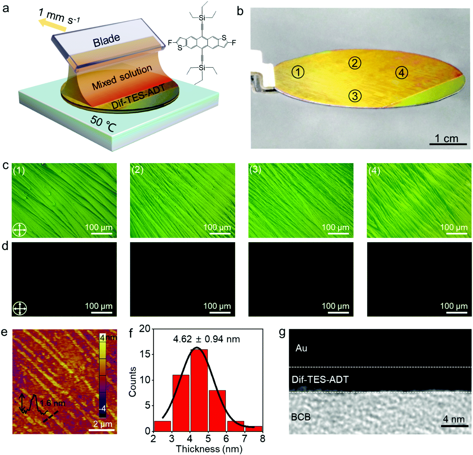 | ||
| Fig. 1 (a) Schematic illustration of the wafer-scale fast deposition of the ultrathin OSC crystalline film. (b) Photograph of the ultrathin Dif-TES-ADT crystalline film captured under cross-polarized light. (c and d) CPOM images of the ultrathin Dif-TES-ADT crystalline film deposited on the wafer. (e) Typical AFM image of the ultrathin Dif-TES-ADT crystalline film. The black line highlights the height profile of the ribbon-shaped crystal on the film surface. (f) Histogram of the thickness distribution of the ultrathin Dif-TES-ADT crystalline films measured from two different samples. 40 positions in these samples were measured, giving rise to an average thickness of 4.62 ± 0.94 nm. (g) Cross-sectional TEM image of the ultrathin Dif-TES-ADT crystalline film. | ||
Next, the crystallinity of the Dif-TES-ADT ultrathin crystalline film was examined through 2D-grazing incidence X-ray diffraction (2D-GIXRD). From the 2D-GIXRD pattern (Fig. 2a), only one diffraction spot can be observed in the out-of-plane direction (qz = 3.86 nm−1), which can be assigned as the (001) plane. The observation of only the first-order peak (001) from the Dif-TES-ADT crystalline film strongly indicates the ultrathin nature of the film. In the in-plane direction (qxy), the clear diffraction spots presented at qy = 9.11 and 10.25 nm−1 can be indexed as (010) and (110), respectively. Fig. 2b and c show the corresponding 1D diffraction profiles with respect to the qz and qxy directions, respectively, extracted from the 2D-GIXRD pattern. In comparison, the spin-coated polycrystalline Dif-TES-ADT film produces diffuse intensities around the (00l) diffraction peaks along with the Debye rings (Fig. S3, ESI†). On the basis of the above 2D-GIXRD data, it can be concluded that the crystallographic orientations of the blade-coated Dif-TES-ADT ultrathin crystalline film are much more ordered than those of the spin-coated polycrystalline film. Further structural characterization of the Dif-TES-ADT ultrathin crystalline film was carried out using a high-resolution atomic force microscope (HR-AFM). HR-AFM images randomly collected from 30 positions on the same sample demonstrate that the Dif-TES-ADT molecules in the film have a very similar packing mode, and the corresponding Fast Fourier Transform (FFT) results show nearly identical patterns (Fig. 2d and e and Fig. S4, ESI†). The lattice constants extracted from such patterns are a = 0.72 ± 0.03 nm, b = 0.73 ± 0.02 nm, and γ = 71.88 ± 2° (Fig. S4, ESI†), which are consistent with the bulk Dif-TES-ADT single crystal.33 The packing orientation of the Dif-TES-ADT molecules in the ultrathin film was further investigated by polarized UV-vis (pUV) absorption (Fig. 2f and g). The pUV absorption spectra were measured, while rotating the polarizer with respect to the blade-coating direction, in order to trace the π–π* transition absorption peaks as a function of the rotation angle. As shown in Fig. 2f, the ultrathin Dif-TES-ADT crystalline film shows absorption peaks at wavelengths of about 420.7, 483.7, 515.4, and 547.5 nm, as were found previously for the Dif-TES-ADT film.34 Among these peaks, the peak at 547.5 nm is corresponding to the π–π* transition. As the polarizer was rotated by 90°, the intensity of this peak decreased gradually, demonstrating a strong anisotropy (Fig. 2g). In particular, when the pUV beam polarization direction was aligned parallel to the growth direction of the Dif-TES-ADT film, a maximum absorption intensity for the π–π* transition was observed. However, when the pUV beam polarization direction was rotated perpendicular to the growth direction of the Dif-TES-ADT film, the peak intensity significantly decreased. This pronounced behavior indicates the anisotropic orientation of Dif-TES-ADT molecules in the ultrathin film; the intermolecular π–π conjugations are mainly oriented along the blade-coating direction, which is highly beneficial for effective charge transport. The above results collectively show that a highly crystalline and ultrathin OSC film has been successfully fabricated at a fast deposition speed of 1 mm s−1, which is higher than that in previous reports (Table S1, ESI†).10,22,24
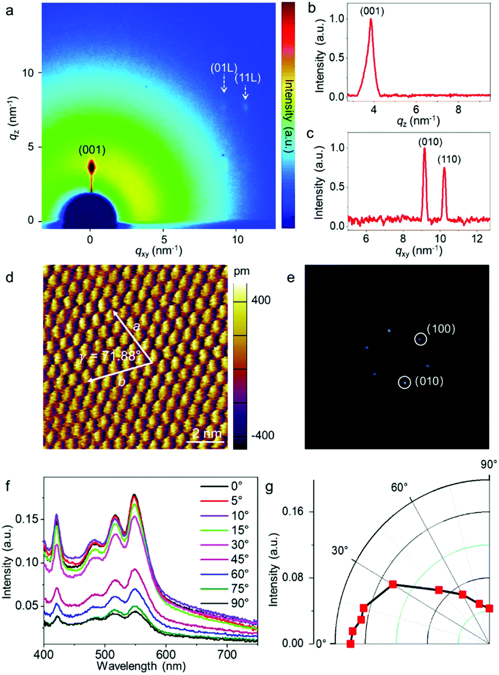 | ||
| Fig. 2 (a) 2D-GIXRD pattern of the ultrathin Dif-TES-ADT crystalline film. (b and c) Corresponding 1D out-of-plane and in-plane profiles. (d and e) HR-AFM image of the ultrathin Dif-TES-ADT crystalline film and the corresponding FFT pattern. (f) pUV absorption spectra of the blade-coated ultrathin Dif-TES-ADT crystalline film. (g) Absorbance dependency of linearly polarized light (547.5 nm) with the polarization direction rotated from 0 to 90°. The coating direction is parallel to the 0° axis of the polarizer. | ||
The influence of the mixed solvents on the morphologies of the Dif-TES-ADT ultrathin crystalline film was then investigated. In these control experiments, Dif-TES-ADT was dissolved in mixtures of o-DCB/m-xylene with different volume ratios at a fixed blade-coating speed of 1 mm s−1. The morphologies of the resultant films were studied using both CPOM and AFM. As shown in Fig. 3, we found a sharp transition in the film morphologies with increasing the volume ratio of o-DCB/m-xylene. When pure m-xylene was used, only discontinuous and thick crystal grains were obtained (Fig. 3a and b). At relatively low o-DCB/m-xylene ratios of 5 v% and 10 v%, many pinholes could be clearly observed in the films (Fig. 3c–f). When the o-DCB content was in the range from 15 to 25 v%, Dif-TES-ADT formed smooth and compact crystalline films (Fig. 3g–l). However, as the o-DCB/m-xylene ratio was increased higher than 25 v%, isotropic and spherulitic films consisting of 1D crystal domains were observed, and these films had obvious topographic defects, such as gaps and pinholes (Fig. 3m–p). At a higher o-DCB concentration, the evaporation rate of the mixed solvent became lower. In this case, the viscous force imposed by the moving blade was dominant over the capillary flow induced by solvent evaporation.35,36 As a result, the solution behind the blade would be dragged out, leading to a longer meniscus (Fig. S5, ESI†). This will induce many more nucleation sites at the front of the meniscus and make the blade lose control of the crystal growth. In the plot of the thickness and surface coverage of the Dif-TES-ADT film versus the o-DCB/m-xylene volume ratio (Fig. 4), it was found that with increasing the o-DCB/m-xylene ratio from 0 to 10 v%, the thickness of the resultant Dif-TES-ADT film dropped from 9.63 to 7.22 nm. Meanwhile the surface coverage of the Dif-TES-ADT film on the substrate increased from 30 to 85%. As the o-DCB/m-xylene ratio was further increased from 15 to 25 v%, the resultant Dif-TES-ADT film became thinner and the substrate could be completely covered by the Dif-TES-ADT film. This scenario shows that the 1D growth mode of the Dif-TES-ADT molecules gradually transformed to a 2D layer-by-layer growth mode with the increase of the o-DCB content.37 When the o-DCB/m-xylene ratio exceeded 30 v%, Dif-TES-ADT molecules would self-assemble into 1D thick and ribbon-like crystals due to the elongated meniscus.
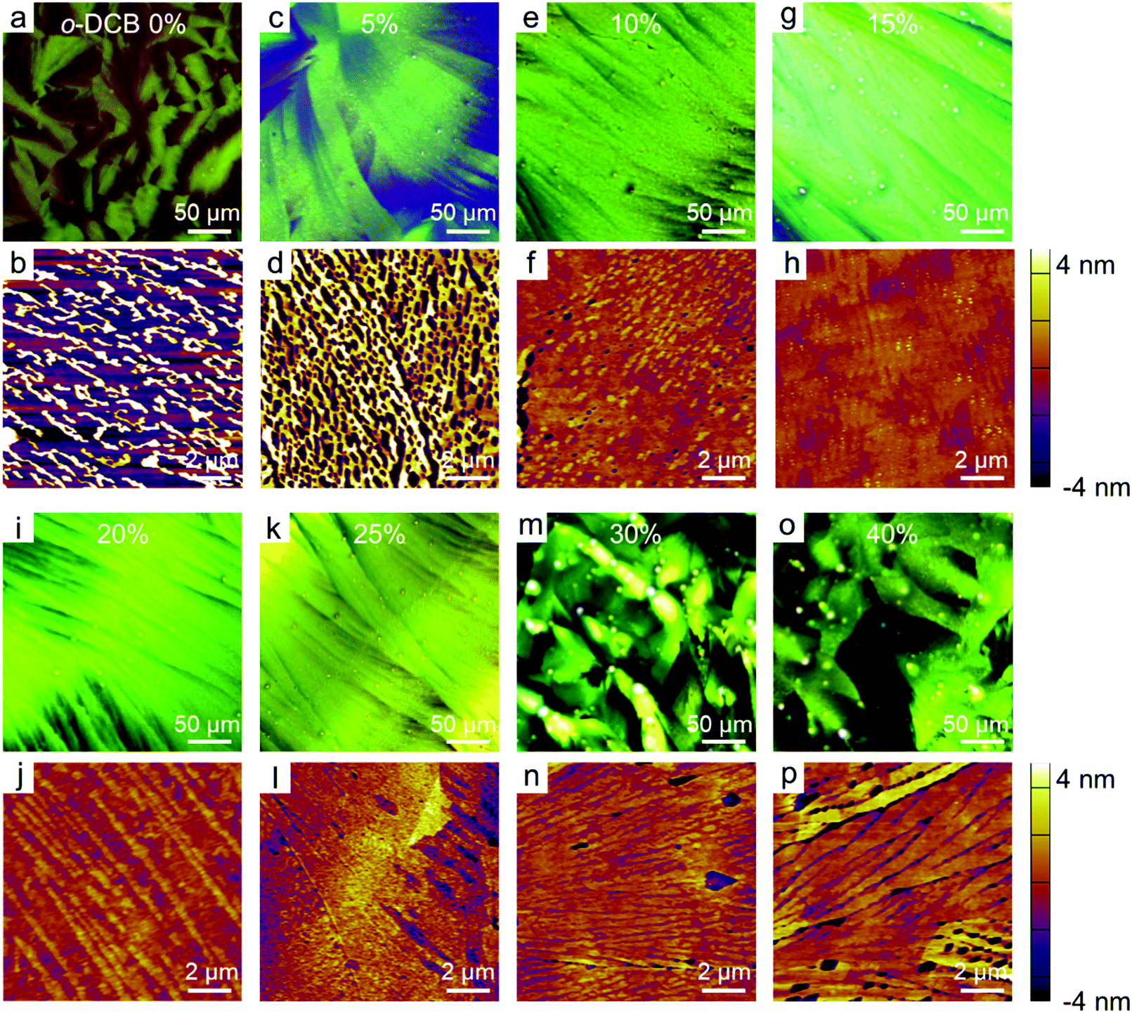 | ||
| Fig. 3 CPOM and AFM images of the Dif-TES-ADT crystalline films obtained from m-xylene/o-DCB solvents with different volume ratios. | ||
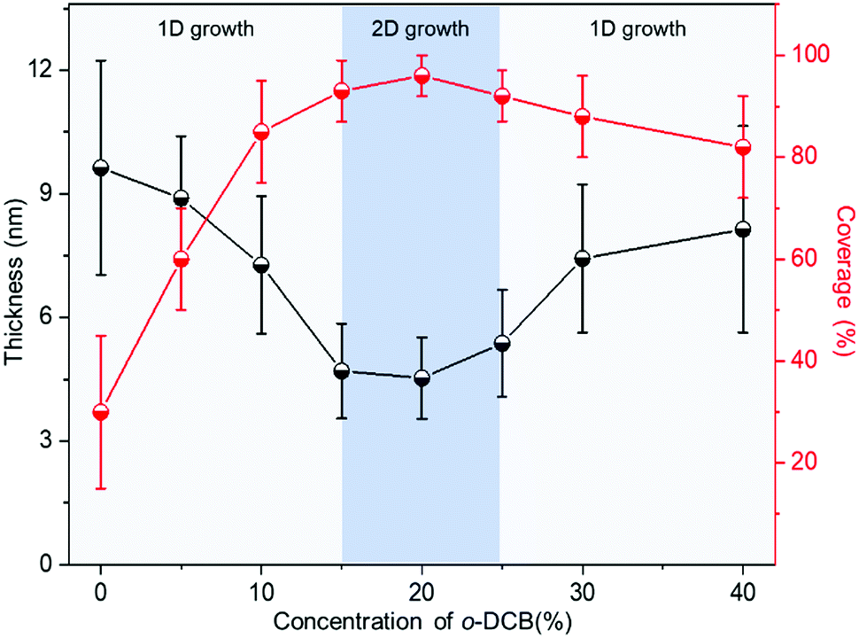 | ||
| Fig. 4 Surface coverage and thickness of the Dif-TES-ADT films with different o-DCB/m-xylene volume ratios. The data are extracted from the AFM measurements. The error bars are computed by averaging 10 different positions on the same sample. | ||
The above results indicate that the use of o-DCB in the mixed solution not only plays a vital role in reducing the structural defects of the OSC films, but also greatly facilitates the 2D assembly of OSC molecules. Accordingly, we compared the different growth mechanisms for the OSC thin films fabricated by using a single solvent and a mixed solvent, as shown in Fig. 5. Previous studies have shown that the optimal blade-coating speed should be close to the crystallization rate of organic semiconductors for the fabrication of high-quality OSC crystals.14,16,21,25,38,39 So, to achieve the fast deposition of OSC crystalline films, rising temperature is a commonly used strategy to increase the crystallization rate of OSCs.17,25,27,38 However, when the substrate is heated, the bottom of the meniscus has a higher temperature than its top (Fig. 5a). The fluid flow inside the meniscus was predicted by COMSOL Multiphysics simulation (details of the COMSOL simulation can be found in the ESI†).20,25,29 It can be seen that temperature-induced convection flow from the higher temperature zone to the lower temperature zone would be generated inside the meniscus, as indicated by the yellow arrows in Fig. 5b. In addition, since the solvent had good wettability on the substrate with a contact angle smaller than 2° (Fig. S6, ESI†), the contact line was strongly pinned by the substrate, and the contact area between the meniscus and the substrate would remain constant at the beginning of the crystal growth process. A capillary flow (indicated by the white arrows in Fig. 5b) of the solvent would occur from its interior to the contact line to replenish the evaporation loss. Under the convection flow and the capillary flow, a vortex formed inside the meniscus. This fluid flow could take molecules away from the contact line (the nucleation sites of molecules), leading to an insufficient supply of organic molecules for nucleation at the contact line (Fig. 5c). The crystallization rate was then reduced accordingly. It is well documented that the optimal blade-coating speed should be close to the crystallization rate of materials to achieve a continuous film.39 When the coating speed is much faster than the crystallization rate, the solution would not fully evaporate after blading, and it will undergo non-uniform crystallization via the “coffee-ring” effect and finally form discontinuous films with crystal domains accompanying many large gaps and pinholes (Fig. 3a).
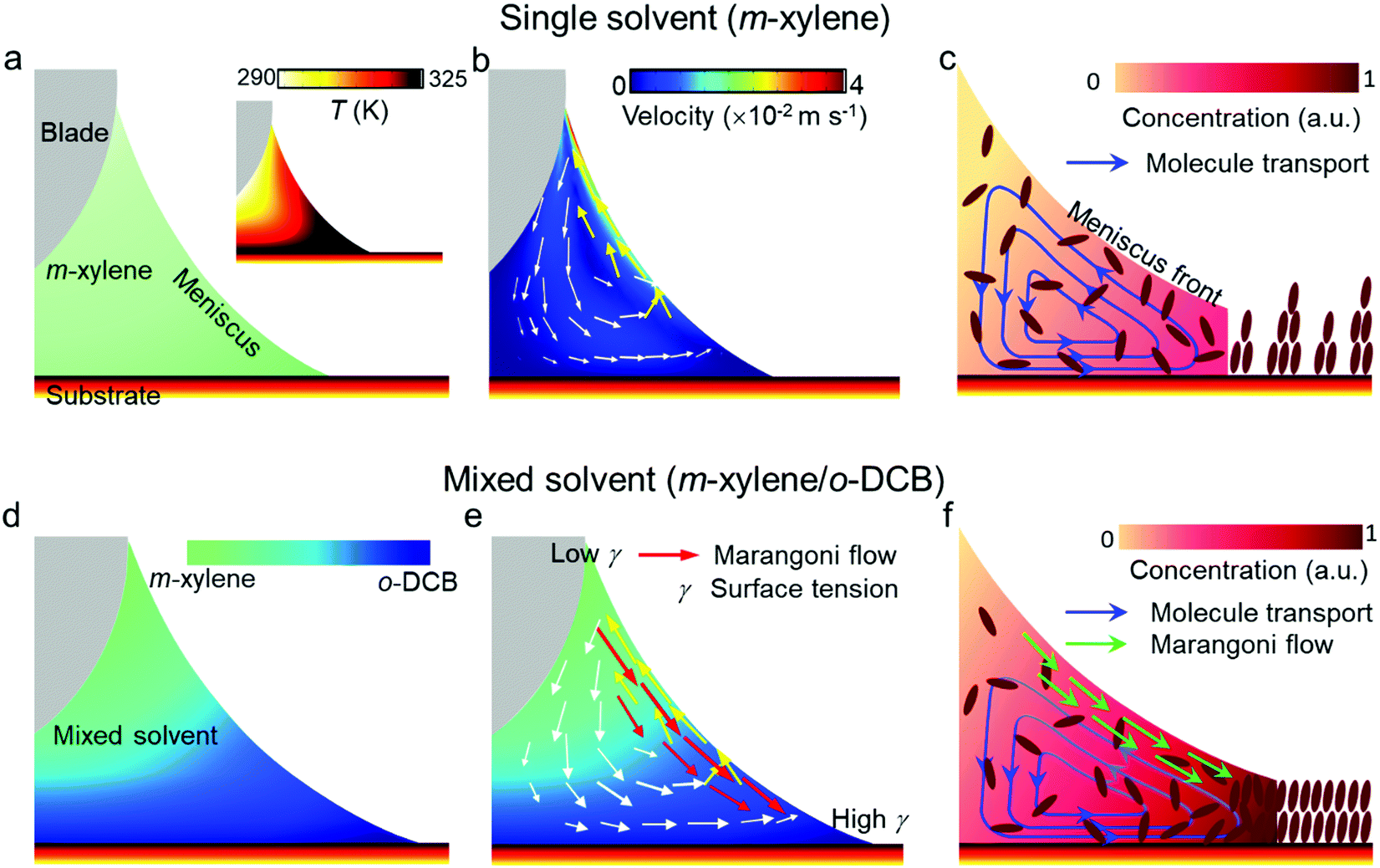 | ||
| Fig. 5 Growth mechanism of the Dif-TES-ADT films in (a–c) a single solvent (m-xylene) and (d–f) a mixed solvent (m-xylene/o-DCB). (a) Meniscus profile of the single solvent m-xylene. The inset shows the simulation result of the temperature distribution in the single solvent meniscus. (b) Simulation result of the velocity distribution in m-xylene. (c) Schematic illustration of molecular aggregation in the meniscus front in m-xylene during blade coating. (d) Solvent composition distribution in the mixed solvent of m-xylene/o-DCB during evaporation. (e) Schematic illustration of the velocity distribution in m-xylene/o-DCB. (f) Schematic illustration of molecular aggregation in the meniscus front of m-xylene/o-DCB during blade coating. | ||
To suppress this fluid flow for the formation of uniform films at a fast coating speed, we introduced another solvent o-DCB with higher surface tension and higher boiling point than m-xylene into the solution. Due to the temperature gradient at the substrate, m-xylene at the bottom of the meniscus would first evaporate. With the loss of m-xylene, more o-DCB appeared at the bottom of the meniscus (Fig. 5d). A surface tension gradient along the air–meniscus interface would induce a Marangoni flow from the lower to higher surface tension regions, as indicated by the red arrows in Fig. 5e. Such Marangoni flow could relieve the temperature-gradient-induced convection flow and draw back some of the molecules from the top of the meniscus to the contact line areas (Fig. 5f). With the enhanced molecule transport to the contact line, the initial gaps and pinholes would be filled, producing high-quality smooth and compact OSC crystalline films. In addition, the crystallization rate was also improved accordingly. On this occasion, fast deposition of a high-quality OSC crystalline thin film was successfully achieved. Although the actual solution growth process is complicated, previous studies have indicated that a high crystallization rate can effectively promote 2D growth of the organic crystals, leading to an enhancement of molecule spread on the substrate.40,41 The mixed solvent system can alter the fluid dynamics by suppressing the initial fluid flow, which not only leads to the formation of uniform pinhole-free films at a fast deposition speed, but also encourages the 2D growth of organic crystals into the ultrathin films. In order to further support the proposed mechanism, other combinations of mixed solvents, m-xylene/2-chlorophenol and m-xylene/iodobenzene, were also used. In these mixed solvents, 2-chlorophenol and iodobenzene both have higher surface tensions and boiling points compared with m-xylene (the properties are listed in Table S2, ESI†). Therefore, a surface tension gradient-induced Marangoni flow could be produced along the meniscus top to the contact line regions. This would also enhance molecule transport toward the contact line and increase the crystallization rate of the OSC. As such, ultrathin Dif-TES-ADT films with thicknesses of 5.22 and 5.86 nm were obtained from the mixed solvents of m-xylene/2-chlorophenol and m-xylene/iodobenzene, respectively, at a fast blade-coating speed of 1 mm s−1 (Fig. S7, ESI†).
To demonstrate the universality of our method, ultrathin crystalline films based on other organic semiconductors, including p-type 6,13-bis(triisopropyl-silylethynyl)pentacene (TIPS-PEN), and 2,6-bis(4-hexylphenyl)anthracene (C6-DPA), and n-type tetrachlorotetraazapentene (4Cl-TIPS-TAP), N,N′-dioctyl-3,4,9,10-perylenedicarboximide (PTCDI-C8), and 6,13-bis((triisopropylsilyl)ethynyl)-5,7,12,14-tetraazapentacene (TIPS-TAP), were also fabricated by using the mixed solvent systems at a fast deposition speed of 1 mm s−1 (Fig. S8, ESI†). The thicknesses of the resultant TIPS-PEN, C6-DPA, 4Cl-TAP, PTCDI-C8, and TIPS-TAP films are measured to be 4.22, 3.87, 7.26, 4.75, and 5.32 nm respectively. Moreover, ultrathin Dif-TES-ADT films with thicknesses of 4.71, 5.34, and 4.25 nm also could be successfully prepared on a glass substrate, Au surface, and poly(ethylenenaphthalate) (PEN) substrate respectively, as shown in Fig. S9, ESI.† These results suggest that the mixed solvent strategy has general applicability in the fast growth of ultrathin OSC crystalline films, and is also applicable to various substrates.
OTFTs were fabricated to investigate the electrical properties of the ultrathin Dif-TES-ADT crystalline film made from the mixed solvent system. OTFTs based on the Dif-TES-ADT films made from pure m-xylene solvent were also fabricated for comparison. All the devices were fabricated in the top-contact, bottom-gate configuration with Au drain and source electrodes (75 nm) and BCB-modified SiO2 dielectric layers. The channel length (L) and width (W) were 25 and 150 μm, respectively (Fig. 6a). Fig. 6b shows the OTFT characteristics of the ultrathin Dif-TES-ADT crystalline film prepared at the optimized volume ratio of o-DCB/m-xylene. The transfer characteristics of the typical device exhibit a small hysteresis and a low threshold voltage (Vth) of about −3 V (Fig. 6b). Besides, the output characteristics show good linearity in the low source–drain voltage (Vds) region (Fig. 6c), which indicates a good ohmic contact between the source/drain electrodes and the ultrathin Dif-TES-ADT crystalline film. The mobility extracted from the saturation regime reaches 5.54 cm2 V−1 s−1, the Ion/Ioff current ratio is ∼105, and the subthreshold slope is about 2.93 V per decade. Fig. 6d plots the mobility distribution of 40 devices (5 × 8 OTFT arrays) on the same substrate. The highest and average mobilities are 5.54 and 3.12 cm2 V−1 s−1, respectively. The transfer characteristics of all the 40 OTFTs are shown in Fig. S10, ESI.† Significantly, the mobilities of the ultrathin Dif-TES-ADT crystalline film exhibit a remarkable improvement compared with that of the film fabricated from pure m-xylene solvent (1.53 cm2 V−1 s−1) (Fig. 6b and Fig. S11, ESI†). Also, the highest mobility of the Dif-TES-ADT ultrathin crystalline film is higher than most previously reported Dif-TES-ADT thin films21,31,42–56 and even is close to that of the reported Dif-TES-ADT single crystals (∼6 cm2 V−1 s−1) (Table S3, ESI†). Furthermore, the contact resistance (Rc) for the ultrathin crystalline film-based OTFT was measured by the transmission line method (TLM) (Fig. S12, ESI†). The channel-width-normalized contact resistance (RcW) for the ultrathin crystalline film-based OTFTs is determined to be 2.2 kΩ cm at a Vg of −45 V, which is 9 times lower than that of the OTFTs fabricated from pure m-xylene solvent (Fig. S12, ESI†). These results unambiguously demonstrate the advantage of the ultrathin OSC crystalline films in the construction of high-performance electronic devices.
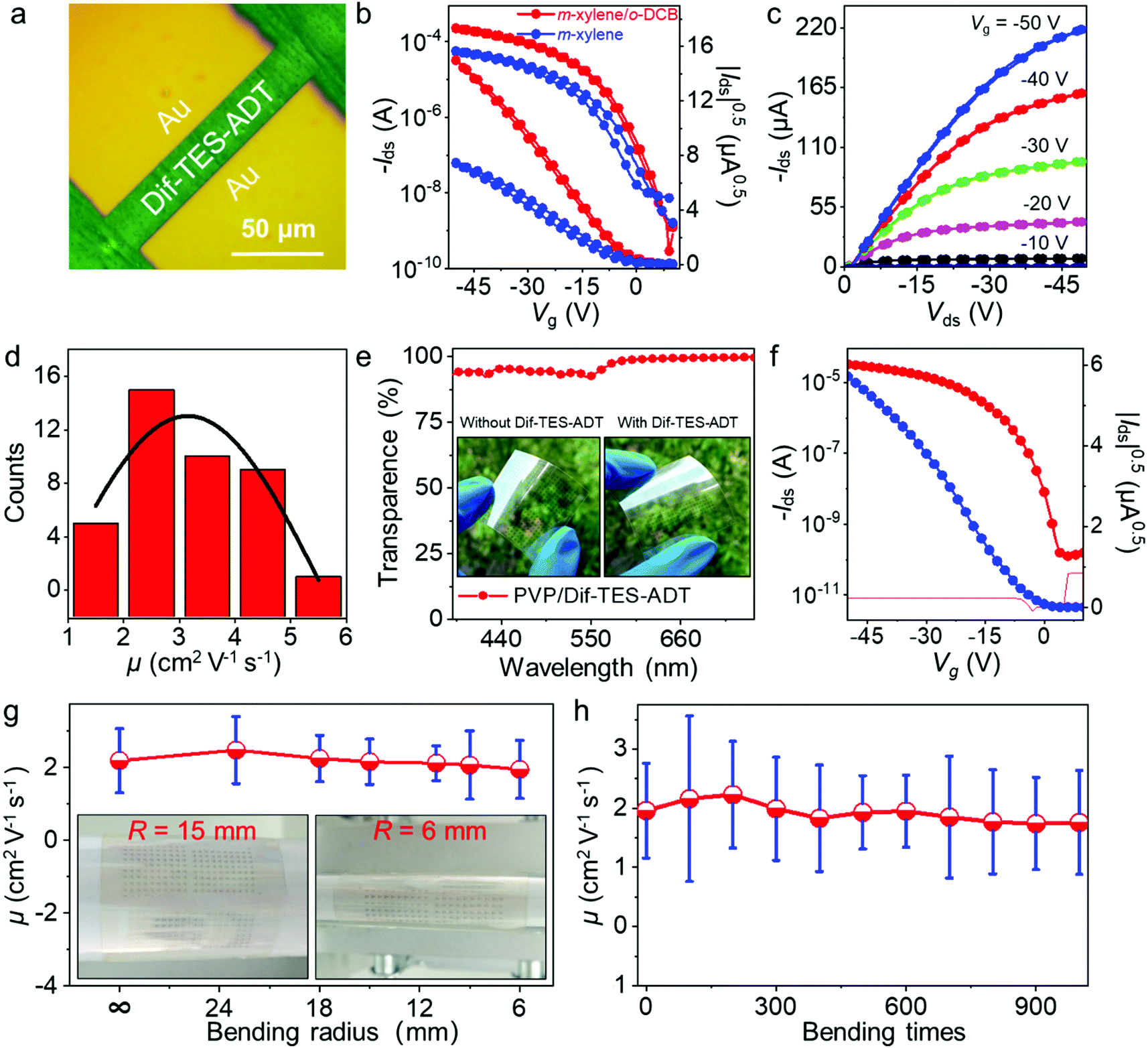 | ||
| Fig. 6 (a) CPOM image of the ultrathin Dif-TES-ADT crystalline film-based OTFT. (b) Comparison of typical OTFT transfer characteristics for the Dif-TES-ADT films fabricated from pure m-xylene solvent and mixed m-xylene/o-DCB solvent, respectively, on BCB/SiO2/Si substrates. (c) Typical output characteristics of the ultrathin Dif-TES-ADT crystalline film-based OTFT. (d) Histogram of hole mobilities measured from the array of 5 × 8 ultrathin Dif-TES-ADT crystalline film-based OTFTs. (e) Transmission spectrum of the ultrathin Dif-TES-ADT crystalline film. Inset: Photographs of corresponding OTFT devices with and without the ultrathin Dif-TES-ADT crystalline film. (f) Typical transfer characteristics of the flexible OTFT device on a PVP substrate. Mobility of the flexible OTFT device as a function of (g) bending radii and (h) bending times. Inset in (g): Photographs of the flexible OTFT device under different bending radii. | ||
Note that the ultrathin Dif-TES-ADT crystalline film shows an excellent transparency of ∼95% in the visible region (Fig. 6e), which is of great interest for flat-panel display backplane applications. Furthermore, compared with thick films or large crystals, ultrathin crystalline films are much softer and thus easily change shape with curved surfaces, giving the corresponding OTFTs excellent flexibility and conformality. To demonstrate the combined merits of the devices with excellent performance, high transparency and outstanding flexibility, we fabricated transparent and flexible OTFTs using the ultrathin Dif-TES-ADT crystalline film as the active layer, cross-linked poly(4-vinylphenol) (PVP) as the dielectric layer, indium tin oxide (ITO) as a gate electrode, and Au as drain and source electrodes. In a flat state, the OTFT exhibits a saturation mobility of 2.64 cm2 V−1 s−1 (Fig. 6f), which is on par with the average mobility of the OTFTs on the rigid SiO2/Si substrate. In addition, the on/off current ratio is 105, the subthreshold slope is about 2 V per decade with a threshold voltage of about −2 V, and hardly any leakage current is observed in the transfer and output characteristics (Fig. 6f and Fig. S13, ESI†). The mechanical flexibility of the OTFTs was further investigated. The electrical characteristics of the flexible OTFTs were recorded in situ under different bending radii (from a flat state to 6 mm). It is observed that the mobility decreases slightly with decreasing the bending radius, revealing a performance degradation of ∼11% of the original value at a bending radius of 6 mm, as shown in Fig. 6g and Fig. S14, ESI.† The variation of the device performance is mainly caused by the degradation of other relatively thick components in the OTFT, including the dielectric, electrodes, and substrate, under the bending-induced mechanical strain. Moreover, the electrical performance of the flexible OTFTs was tested after multiple bending stresses. At a small bending radius of 6 mm, the mobility of the device changes only very slightly even after 1000 bending times (Fig. 6h and Fig. S15, ESI†). We note that the mobilities of the flexible OTFTs can exceed 1.0 cm2 V−1 s−1 during the whole bending process, which is actually high enough for a variety of applications in sensors, wearable devices, electronic skin, and drivers for images.
3. Conclusions
In conclusion, we demonstrate that a mixed solvent system of m-xylene/o-DCB can obviously improve the blade-coating quality of Dif-TES-ADT ultrathin crystalline films at a fast coating speed. Wafer-scale pinhole-free Dif-TES-ADT ultrathin crystalline films were demonstrated. The addition of o-DCB with higher surface tension and lower volatility than m-xylene could introduce a surface tension gradient in the solution and remarkably enhance the mass transport of molecules towards the contact line. As a result, the crystallization rate of Dif-TES-ADT molecules would be remarkably improved, enabling fast 2D layer-by-layer growth of ultrathin Dif-TES-ADT films at a rate of ∼1 mm s−1. 2D-GIXRD and pUV absorption spectroscopy verified the highly crystalline nature and ordered molecular packing of the ultrathin films. Significantly, OTFTs based on the Dif-TES-ADT ultrathin crystalline film exhibited an increased mobility of 5.54 cm2 V−1 s−1, which is close to that of the Dif-TES-ADT single crystal-based devices and higher than that of most Dif-TES-ADT film-based devices. Benefiting from the ultrathin nature, transparent and flexible OTFTs based on the ultrathin Dif-TES-ADT film were demonstrated. We showed that this methodology could be used to quickly deposit various kinds of ultrathin OSC crystalline films, making it potentially suitable for the upscaling of device fabrication for mass production.4. Experimental
Materials
Dif-TES-ADT (Lumtec), TIPS-pentacene (Lumtec), TIPS-TAP (Lumtec), C6-DPA (Lumtec), PTCDI-C8 (Sigma), o-DCB (Aldrich, HPLG), m-xylene (Aldrich, HPLG), 2-chlorophenol (J&K), iodobenzene (J&K), OTS (Aldrich, HPLG), and BCB (Dow Chemicals) were purchased and used without further purification. 4Cl-TAP was provided by Prof. Qian Miao's group.Deposition of ultrathin OSC crystalline films
A homemade blade-coating setup was assembled, which included an OTS-treated SiO2/Si blade, a horizontal translation stage with a speed controller to program the movement of the blade, and a heater with temperature feedback to heat up the substrate. During the shearing process, the temperature of the substrate surface was kept at 50 °C, and the gap between the blade and substrate surface was ∼0.1 mm. ∼5 μL Dif-TES-ADT solution (2 mg mL−1) was dropped into the gap and the blade was pulled at a constant speed on the moving stage. An ultrathin Dif-TES-ADT crystalline film will be deposited on the substrate.Characterization of the ultrathin OSC crystalline films
Microscopic images were taken by using an optical microscope with a cross polarizer (Olympus BX51). UV-vis absorption spectra were recorded on a HITACHI U-3900 spectrophotometer. AFM images were recorded on a tapping-mode AFM (Asylum Research). TEM was performed by using an FEI TecnaiG2 20 STEM system. 2D-GIXRD measurements were performed at the BL14B1 beam line (energy = 10 keV) at Shanghai Synchrotron Radiation Facility. The grazing-incidence angle for all measurements was 0.2°. The sample-to-detector distance (SDD) was 425 mm and the diffraction patterns were mostly acquired for 120 s with a 2D charge-coupled device (CCD) detector.Device fabrication and characterization
Au source/drain electrode pairs were deposited by thermal evaporation through a metal shadow mask to create OTFTs with channel length L = 25 μm and width W = 150 μm. ITO/PET substrates for flexible OTFTs were cleaned with isopropyl alcohol and deionized water for 10 min each, and then exposed to UV-ozone for 30 min. Subsequently, a cross-linked PVP layer was prepared by spin-coating a solution containing 11 wt% PVP and 4.7 wt% poly(melamine-co-formaldehyde) methylated in propylene glycol monomethyl ether acetate solvent on the substrate at 1500 rpm for 20 s. The resultant PVP layer was thermally annealed at 160 °C for 2 h. The fabrication of the ultrathin Dif-TES-ADT crystalline film and Au S/D electrodes for bottom-gate top-contact OTFT arrays followed the sample procedures on the rigid substrates. For Rc measurements, devices with different channel lengths from 40 to 200 μm were utilized in the TLM (Fig. S12a, ESI†). To accurately estimate the conduction currents, the channel bars and square contact pads were cut off by a probe tip. The corresponding transfer curves in the linear regimes at each L were measured at a Vds of −5 V and are plotted in Fig. S12c, ESI.† The channel-width-normalized total resistance (RtW) as a function of the channel length is plotted in Fig. S12b, ESI.† The channel-width-normalized contact resistance (RcW) could be obtained from the intercept with the y-axis by extrapolating the linear fit. All the electrical measurements were performed under ambient conditions at room temperature by using a Keithley 4200-SCS semiconductor parameter analyzer on a probe station (M150, Cascade).Conflicts of interest
There are no conflicts to declare.Acknowledgements
This work was supported by the National Natural Science Foundation of China (Grant No. 51821002, 91833303, 61904117, 51973147, and 51672180), the Natural Science Foundation of Jiangsu Province of China (BK20180845), the Priority Academic Program Development of Jiangsu Higher Education Institutions (PAPD), the 111 Project, and Collaborative Innovation Center of Suzhou Nano Science and Technology (Nano-CIC). The authors also thank the Beamline BL14B1 (Shanghai Synchrotron Radiation Facility) for providing the beam time.Notes and references
- T. Liu, J. Zhao, W. Xu, J. Dou, X. Zhao, W. Deng, C. Wei, W. Xu, W. Guo and W. Su, Nanoscale, 2018, 10, 614 RSC.
- D. Ji, T. Li, Y. Zou, M. Chu, K. Zhou, J. Liu, G. Tian, Z. Zhang, X. Zhang and L. Li, Nat. Commun., 2018, 9, 2339 CrossRef PubMed.
- W. Deng, X. Zhang, H. Dong, J. Jie, X. Xu, J. Liu, L. He, L. Xu, W. Hu and X. Zhang, Mater. Today, 2019, 24, 17 CrossRef CAS.
- J. Xu, S. Wang, G.-J. N. Wang, C. Zhu, S. Luo, L. Jin, X. Gu, S. Chen, V. R. Feig and J. W. To, Science, 2017, 355, 59 CrossRef CAS PubMed.
- S. Wang, J. Xu, W. Wang, G. N. Wang, R. Rastak, F. Molina-Lopez, J. W. Chung, S. Niu, V. R. Feig, J. Lopez, T. Lei, S. K. Kwon, Y. Kim, A. M. Foudeh, A. Ehrlich, A. Gasperini, Y. Yun, B. Murmann, J. B. Tok and Z. Bao, Nature, 2018, 555, 83 CrossRef CAS PubMed.
- N. M. Murari, Y.-J. Hwang, F. S. Kim and S. A. Jenekhe, Org. Electron., 2016, 31, 104 CrossRef CAS.
- S. C. Mannsfeld, B. C. Tee, R. M. Stoltenberg, C. V. H. Chen, S. Barman, B. V. Muir, A. N. Sokolov, C. Reese and Z. Bao, Nat. Mater., 2010, 9, 859 CrossRef CAS PubMed.
- L. Li, P. Gao, M. Baumgarten, K. Mullen, N. Lu, H. Fuchs and L. Chi, Adv. Mater., 2013, 25, 3419 CrossRef CAS PubMed.
- X. Zhang, J. Mao, W. Deng, X. Xu, L. Huang, X. Zhang, S. T. Lee and J. Jie, Adv. Mater., 2018, 30, 1800187 CrossRef PubMed.
- A. Yamamura, S. Watanabe, M. Uno, M. Mitani, C. Mitsui, J. Tsurumi, N. Isahaya, Y. Kanaoka, T. Okamoto and J. Takeya, Sci. Adv., 2018, 4, eaao5758 CrossRef PubMed.
- Q. Wang, S. Jiang, J. Qian, L. Song, L. Zhang, Y. Zhang, Y. Zhang, Y. Wang, X. Wang, Y. Shi, Y. Zheng and Y. Li, Sci. Rep., 2017, 7, 7830 CrossRef PubMed.
- Z. Lin, X. Guo, L. Zhou, C. Zhang, J. Chang, J. Wu and J. Zhang, Org. Electron., 2018, 54, 80 CrossRef CAS.
- W. Deng, X. Zhang, R. Jia, L. Huang, X. Zhang and J. Jie, NPG Asia Mater., 2019, 11, 77 CrossRef CAS.
- W. Zhao, J. Jie, Q. Wei, Z. Lu, R. Jia, W. Deng, X. Zhang and X. Zhang, Adv. Funct. Mater., 2019, 29, 1902494 CrossRef.
- L. Wang, X. Zhang, G. Dai, W. Deng, J. Jie and X. Zhang, Nano Res., 2018, 11, 882 CrossRef CAS.
- M. R. Niazi, R. Li, E. Q. Li, A. R. Kirmani, M. Abdelsamie, Q. Wang, W. Pan, M. M. Payne, J. E. Anthony and D.-M. Smilgies, Nat. Commun., 2015, 6, 8598 CrossRef CAS PubMed.
- G. Giri, E. Verploegen, S. C. Mannsfeld, S. Atahan-Evrenk, D. H. Kim, S. Y. Lee, H. A. Becerril, A. Aspuru-Guzik, M. F. Toney and Z. Bao, Nature, 2011, 480, 504 CrossRef CAS PubMed.
- Z. Qi, J. Cao, H. Li, L. Ding and J. Wang, Adv. Electron. Mater., 2015, 1, 1500173 CrossRef.
- H. Ren, N. Cui, Q. Tang, Y. Tong, X. Zhao and Y. Liu, Small, 2018, 14, 1801020 CrossRef PubMed.
- Z. Zhang, B. Peng, X. Ji, K. Pei and P. K. L. Chan, Adv. Funct. Mater., 2017, 27, 1703443 CrossRef.
- M. R. Niazi, R. Li, M. Abdelsamie, K. Zhao, D. H. Anjum, M. M. Payne, J. Anthony, D. M. Smilgies and A. Amassian, Adv. Funct. Mater., 2016, 26, 2371 CrossRef CAS.
- S. Arai, S. Inoue, T. Hamai, R. Kumai and T. Hasegawa, Adv. Mater., 2018, 30, e1707256 CrossRef PubMed.
- D. Khim, G. S. Ryu, W. T. Park, H. Kim, M. Lee and Y. Y. Noh, Adv. Mater., 2016, 28, 2752 CrossRef CAS PubMed.
- B. Peng, S. Huang, Z. Zhou and P. K. L. Chan, Adv. Funct. Mater., 2017, 27, 1700999 CrossRef.
- B. Peng, Z. Wang and P. K. L. Chan, J. Mater. Chem. C, 2016, 4, 8628 RSC.
- F. Zhang, C. a. Di, N. Berdunov, Y. Hu, Y. Hu, X. Gao, Q. Meng, H. Sirringhaus and D. Zhu, Adv. Mater., 2013, 25, 1401 CrossRef CAS PubMed.
- Z. Zhou, Z. Zhang, Q. Wu, X. Ji, J. Wang, X. Zeng, S.-P. Feng and P. K. L. Chan, ACS Appl. Mater. Interfaces, 2018, 10, 35395 CrossRef CAS PubMed.
- H. A. Becerril, M. E. Roberts, Z. Liu, J. Locklin and Z. Bao, Adv. Mater., 2008, 20, 2588 CrossRef CAS.
- X. Gu, L. Shaw, K. Gu, M. F. Toney and Z. Bao, Nat. Commun., 2018, 9, 534 CrossRef PubMed.
- S. Galindo, A. Tamayo, F. Leonardi and M. Mas-Torrent, Adv. Funct. Mater., 2017, 27, 1700526 CrossRef.
- A. Pérez-Rodríguez, I. S. Temiño, C. Ocal, M. Mas-Torrent and E. Barrena, ACS Appl. Mater. Interfaces, 2018, 10, 7296 CrossRef PubMed.
- K. Kim, J. Bae, S. H. Noh, J. Jang, S. H. Kim and C. E. Park, J. Phys. Chem. Lett., 2017, 8, 5492 CrossRef CAS PubMed.
- O. D. Jurchescu, S. Subramanian, R. J. Kline, S. D. Hudson, J. E. Anthony, T. N. Jackson and D. J. Gundlach, Chem. Mater., 2008, 20, 6733 CrossRef CAS.
- B. T. Lim, J. Cho, K. H. Cheon, K. Shin and D. S. Chung, Org. Electron., 2015, 18, 113 CrossRef CAS.
- B. Song, K. Sneha, J. Gu, K. Zhang, A. Reese, Y. Ying, L. Wang, H. Wang, Y. Li, M. Wang, S. Lu, X. Hao, X. Li, B. Xu. and X. Li, Nat. Commun., 2018, 9, 534 CrossRef PubMed.
- S. K. Park, J. J. Kwok, R. Dilmurat, G. Qu, P. Kafle, X. Luo, S. Jung, Y. Oliver, J. Lee, J. Mei, D. Beljoone and Y. Diao, Sci. Adv., 2019, 5, eaaw7757 CrossRef PubMed.
- B. Kang, M. Jang, Y. Chung, H. Kim, S. K. Kwak, J. H. Oh and K. Cho, Nat. Commun., 2014, 5, 4752 CrossRef CAS PubMed.
- J. Chang, C. Chi, J. Zhang and J. Wu, Adv. Mater., 2013, 25, 6442 CrossRef CAS PubMed.
- R. Janneck, F. Vercesi, P. Heremans, J. Genoe and C. Rolin, Adv. Mater., 2016, 28, 8007 CrossRef CAS PubMed.
- P. Hartman and P. Bennema, J. Cryst. Growth, 1980, 49, 145 CrossRef CAS.
- Q. Wang, J. Qian, Y. Li, Y. Zhang, D. He, S. Jiang, Y. Wang, X. Wang, L. Pan and J. Wang, Adv. Funct. Mater., 2016, 26, 3191 CrossRef CAS.
- C. Pitsalidis, A.-M. Pappa, S. Hunter, M. M. Payne, J. E. Anthony, T. D. Anthopoulos and S. Logothetidis, ACS Appl. Mater. Interfaces, 2015, 7, 6496 CrossRef CAS PubMed.
- N. A. Azarova, J. W. Owen, C. A. McLellan, M. A. Grimminger, E. K. Chapman, J. E. Anthony and O. D. Jurchescu, Org. Electron., 2010, 11, 1960 CrossRef CAS.
- P. J. Diemer, C. R. Lyle, Y. Mei, C. Sutton, M. M. Payne, J. E. Anthony, V. Coropceanu, J. L. Brédas and O. D. Jurchescu, Adv. Mater., 2013, 25, 6956 CrossRef CAS PubMed.
- S. K. Park, D. A. Mourey, S. Subramanian, J. E. Anthony and T. N. Jackson, Appl. Phys. Lett., 2008, 93, 274 Search PubMed.
- S. K. Park, D. A. Mourey, S. Subramanian, J. E. Anthony and T. N. Jackson, IEEE Electron Device Lett., 2008, 29, 1004 CAS.
- S. Subramanian, S. K. Park, S. R. Parkin, V. Podzorov, T. N. Jackson and J. E. Anthony, J. Am. Chem. Soc., 2008, 130, 2706 CrossRef CAS PubMed.
- A. Pierre, M. Sadeghi, M. M. Payne, A. Facchetti, J. E. Anthony and A. C. Arias, Adv. Mater., 2014, 26, 5722 CrossRef CAS PubMed.
- I. Temiño, F. G. Del Pozo, M. Ajayakumar, S. Galindo, J. Puigdollers and M. Mas-Torrent, Adv. Mater. Technol., 2016, 1, 1600090 CrossRef.
- Q. Zhang, F. Leonardi, S. Casalini, I. Temiño and M. Mas-Torrent, Sci. Rep., 2016, 6, 39623 CrossRef CAS PubMed.
- K. Zhao, O. Wodo, D. Ren, H. U. Khan, M. R. Niazi, H. Hu, M. Abdelsamie, R. Li, E. Q. Li and L. Yu, Adv. Funct. Mater., 2016, 26, 1737 CrossRef CAS.
- S. Hunter, J. Chen and T. D. Anthopoulos, Adv. Funct. Mater., 2014, 24, 5969 CrossRef CAS.
- N. Shin, J. Kang, L. J. Richter, V. M. Prabhu, R. J. Kline, D. A. Fischer, D. M. DeLongchamp, M. F. Toney, S. K. Satija and D. J. Gundlach, Adv. Funct. Mater., 2013, 23, 366 CrossRef CAS.
- J. Smith, W. Zhang, R. Sougrat, K. Zhao, R. Li, D. Cha, A. Amassian, M. Heeney, I. McCulloch and T. D. Anthopoulos, Adv. Mater., 2012, 24, 2441 CrossRef CAS PubMed.
- R. Hamilton, J. Smith, S. Ogier, M. Heeney, J. E. Anthony, I. McCulloch, J. Veres, D. D. Bradley and T. D. Anthopoulos, Adv. Mater., 2009, 21, 1166 CrossRef CAS.
- J. Smith, R. Hamilton, M. Heeney, D. M. de Leeuw, E. Cantatore, J. E. Anthony, I. McCulloch, D. D. Bradley and T. D. Anthopoulos, Appl. Phys. Lett., 2008, 93, 448 Search PubMed.
Footnote |
| † Electronic supplementary information (ESI) available. See DOI: 10.1039/d0nh00096e |
| This journal is © The Royal Society of Chemistry 2020 |