DOI:
10.1039/C9NH00341J
(Communication)
Nanoscale Horiz., 2019,
4, 1293-1301
Fully transparent, flexible and waterproof synapses with pattern recognition in organic environments†
Received
23rd May 2019
, Accepted 10th June 2019
First published on 11th June 2019
Abstract
Artificial intelligence applications require bio-inspired neuromorphic systems that consist of electronic synapses (e-synapses) able to perform learning and memory functions. However, all transparent and flexible organic e-synapses have the disadvantage of being easily dissolvable in water or organic solutions. In the present work, a stable waterproof artificial synapse based on a fully transparent electronic device, suitable for wearable applications in organic environments is for the first time demonstrated. Essential synaptic behaviors, including paired-pulse facilitation (PPF), long-term potentiation/depression (LTP/LTD), and learning–forgetting–relearning, were successfully emulated. The artificial synaptic device could achieve an optical transmittance of ∼87.5% in the visible light range, which demonstrated reliable long-term potentiation/depression under bent states with a bending radius of 5 mm. After being immersed in water and 5 types of common organic solvents for over 12 hours, the e-synapse could function with 6000 spikes without noticeable degradation in the organic environment. The neural network was constructed from e-synapses with controllable weights update and a device-to-system level simulation framework was developed with a recognition rate of 92.4%, which demonstrated the feasibility of highly transparent, biocompatible, flexible, and waterproof e-synapses used in artificial intelligence systems.
New concepts
Brain-inspired neuromorphic computational systems composed of e-synapses have shown great potential in artificial intelligence applications beyond the standard von Neumann architecture. The next-generation electronic synapses need to be suitable for multiple application scenarios including wearable, “see-through” and implantable electronics, even in organic environments. However, it's difficult to realize these functions in a single synaptic device. By careful design of the material system, we realize waterproof function and pattern recognition application on an array of wearable, biocompatible and fully transparent artificial synapses for the first time. The novel synaptic device could resist short-period damage by water and organic reagents and could be applied in organic environments.
|
Introduction
The human brain is able to learn, memorize, and perform complex calculations with extremely low energy consumption, inspiring the construction of neuromorphic computing systems able to emulate the function of the brain.1 Novel neuromorphic computing systems are able to overcome the limitations of the classical von Neumann architecture and thereby have become a strong competitor as a new computing paradigm. In the human brain, synapses with plasticity are the basic units of neural networks.2,3 Versatile synaptic functions have been successfully simulated using a single physical device.4–6 Such devices with modulated conductance can be repeatedly distributed to form an array, which is called an artificial neural network. Based on this network, various applications of artificial intelligence have been developed, such as AlphaGo (learning the game of Go), face unlock, and others.7,8 Edge computing is a new technology which calls for data processing that occurs at the edge of the network to solve the problems of latency, security and bandwidth costs. A transparent artificial synaptic device could be integrated into a display and finish computing task in a part of the display. The wide use of novel artificial intelligence devices is inseparable from the development of flexible, transparent, and even biocompatible electronics for pattern recognition, which paves the way for the implementation of next-generation, wearable, “invisible”, and implantable synaptic systems.4,9–13 However, it's hard to integrate the features of full transparency, flexibility and biocompatibility for resisting organic environments in a single artificial synapse due to the inherent characteristics of materials.
In terms of the materials used for the substrate, functional layer, and electrodes, mechanically robust and transparent characteristics are required. The electrodes of most flexible memories are based on opaque metals (e.g., Pt, Au, Cu, and Al), which are not suitable for transparent devices.14–16 Furthermore, most functional transparent materials are metal oxides with wide band gaps (e.g., HfO2, ZrO2, and ZnO), which are not biocompatible17–19 and not beneficial to the development of bio-integrated and implantable electronics.11–13 In order to overcome the aforementioned challenges, attention has been turned to indium tin oxide (ITO) electrodes and stretchable-biocompatible organic polymers. Various novel organic materials have been investigated for the development of artificial synaptic devices, such as chitosan, lignin, P(VDF-TrFE), and polymethyl methacrylate (PMMA).1,5,20–22 However, according to previous studies, these organic semiconductor materials are easily dissolved in water or organic solvents, becoming a bottleneck in the development of organic-based devices.23–28 One of the most promising candidates for functional materials with great transparency, flexibility, and biocompatibility is poly(3,4-ethylenedioxythiophene)/poly-styrene sulfonate (PEDOT/PSS), which has been reported to have been used in electronic plants (implanted in garden roses), as well as in wearable devices or optoelectronics.29–32 It is worth mentioning that PEDOT is hydrophobic and PEDOT:PSS films can crystallize after solvent evaporation.33–35 PEDOT:PSS films with the advantage of high transparency and biocompatibility would not dissolve after immersion in most organic solvents, with the potential to be integrated into a reliable artificial synaptic device.
By carefully designing the structure of the device, a transparent, flexible, biocompatible, and waterproof device (ITO/PEDOT/PSS/ITO) with pattern recognition function, able to prevent degradation of organic solvents, is for the first time proposed. Synaptic behaviors including excitatory/inhibitory postsynaptic current (EPSC/IPSC), paired-pulse facilitation (PPF), long-term potentiation/depression (LTP/LTD), and “learning–forgetting–relearning” behaviors36–39 were demonstrated at the device level. After treatment with water and organic solvents including N,N-dimethylformamide (DMF), acetone (AR), ethanol, methanol, and toluene for over 12 hours, the artificial synapses were still working normally. The stable chemical properties of the developed device could overcome the limitations of traditional organic materials such as PMMA, P(VDF-TrFE), and pentacene, which are easily dissolved in AR, DMF, and toluene, respectively, indicating the potential of this device to be used in organic environments. Based on the developed reliable device, a large-scale artificial neural network was successfully emulated, reaching a handwritten digit recognition rate of 92.4%.
Results and discussion
The fully transparent artificial synapse
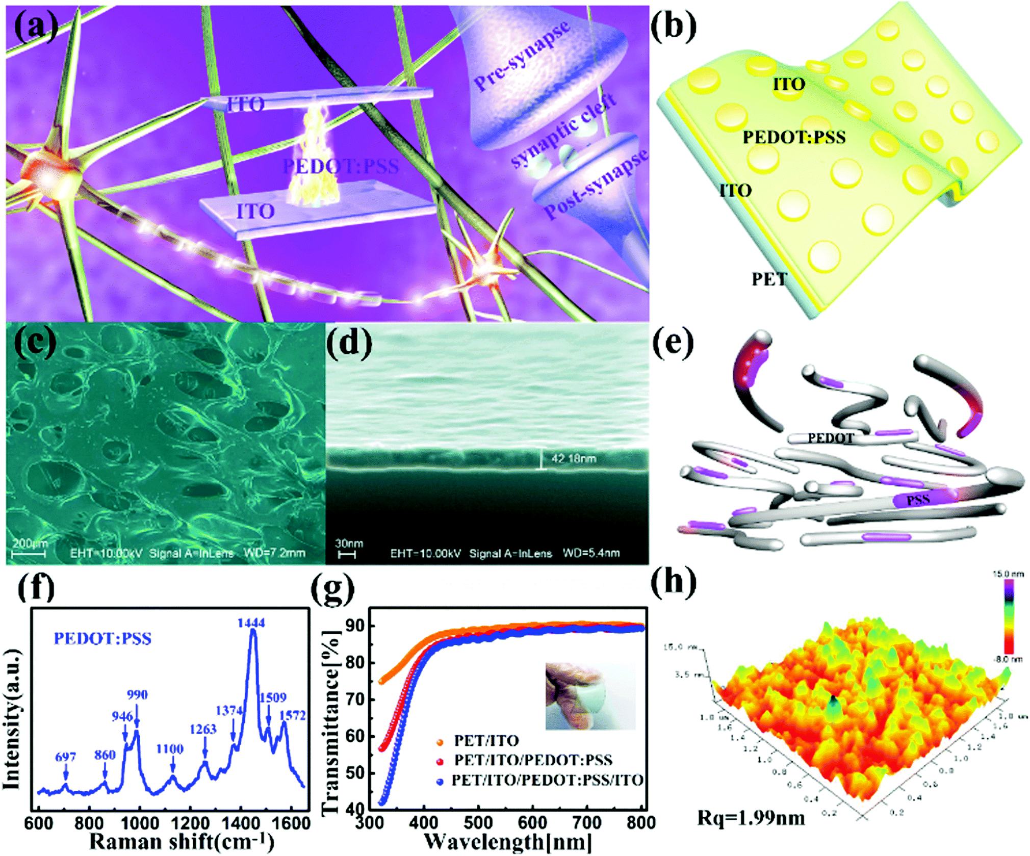
Fully transparent and flexible electronics have drawn attention for applications in optoelectronics, portable displays, and “invisible” wearable products.40–43 For the development of transparent and flexible electronics with synaptic plasticity, highly transparent and stretchable PEDOT:PSS was chosen as the functional layer. Schematic diagrams of a bio-synapse and flexible electronic synapses (e-synapses) are presented in Fig. 1a and b, respectively. After spin-coating and sputtering (Fig. 2a), the active layer of PEDOT:PSS with a roughness of 1.99 nm was sandwiched between identical ITO electrodes (Fig. 1h). The network structure film had a thickness of 42.18 nm, as can be seen in the planar and cross-sectional scanning electron microscopy (SEM) views in Fig. 1c and d, respectively. In the PEDOT:PSS polymer, PEDOT was attached to PSS by ionic interactions (Fig. 1e), which could transform from a non-conductive state (PEDOT0) to an electrically conductive state (PEDOT+) by hole injection.44 The chemical structure of the PEDOT:PSS film was analyzed by Raman spectra in the wavenumber range of 600–1600 cm−1 (Fig. 1f). The typical vibration modes situated at 1572 and 1509 cm−1 were assigned to the asymmetric Cα![[double bond, length as m-dash]](https://www.rsc.org/images/entities/char_e001.gif) Cβ stretching, while the intense peak at 1444 cm−1 originated from the symmetrical stretching of CαCβ. The peaks from Cβ–Cβ stretching, Cα–Cα′ inter-ring stretching, C–O–C deformation, and C–S–C bending were located at 1374, 1263, 1100, and 697 cm−1, respectively. Moreover, the rest of the peaks (at 990, 946, and 860 cm−1) could be attributed to oxyethylene ring deformation, which was consistent with previous reports.45,46 The PEDOT:PSS-based device could achieve 87.5% transparency at 550 nm wavelength, which was in the visible range of the human eye.12 The transmittance of the fabricated device with electrodes had no obvious reduction compared to the PET/ITO substrate (89.5%) and the PEDOT:PSS spin-coated substrate (88.6%), as shown in Fig. 1g.
Cβ stretching, while the intense peak at 1444 cm−1 originated from the symmetrical stretching of CαCβ. The peaks from Cβ–Cβ stretching, Cα–Cα′ inter-ring stretching, C–O–C deformation, and C–S–C bending were located at 1374, 1263, 1100, and 697 cm−1, respectively. Moreover, the rest of the peaks (at 990, 946, and 860 cm−1) could be attributed to oxyethylene ring deformation, which was consistent with previous reports.45,46 The PEDOT:PSS-based device could achieve 87.5% transparency at 550 nm wavelength, which was in the visible range of the human eye.12 The transmittance of the fabricated device with electrodes had no obvious reduction compared to the PET/ITO substrate (89.5%) and the PEDOT:PSS spin-coated substrate (88.6%), as shown in Fig. 1g.
 |
| | Fig. 1 Structure and materials of the transparent and flexible synapses. (a) Illustration of the identical bio-synapse and artificial synapse structures. The two electrodes and the functional layer correspond to pre-synapse, post-synapse, and synaptic cleft, respectively. (b) Schematic of the ITO/PEDOT:PSS/ITO flexible and transparent artificial synaptic device. (c) Top and (d) cross-sectional SEM images of the PEDOT:PSS film on the Si substrate. The film thickness was 42.18 nm. (e) Schematic structure and (f) Raman spectra of PEDOT:PSS. (g) Transmittance spectrum of the PET/ITO, PET/ITO/PEDOT:PSS, and PET/ITO/PEDOT:PSS/ITO structures. (h) AFM image (2 × 2 μm2) of the PEDOT:PSS film on the PET/ITO substrate. Root-mean-square average roughness (Rq) was 1.99 nm. | |
 |
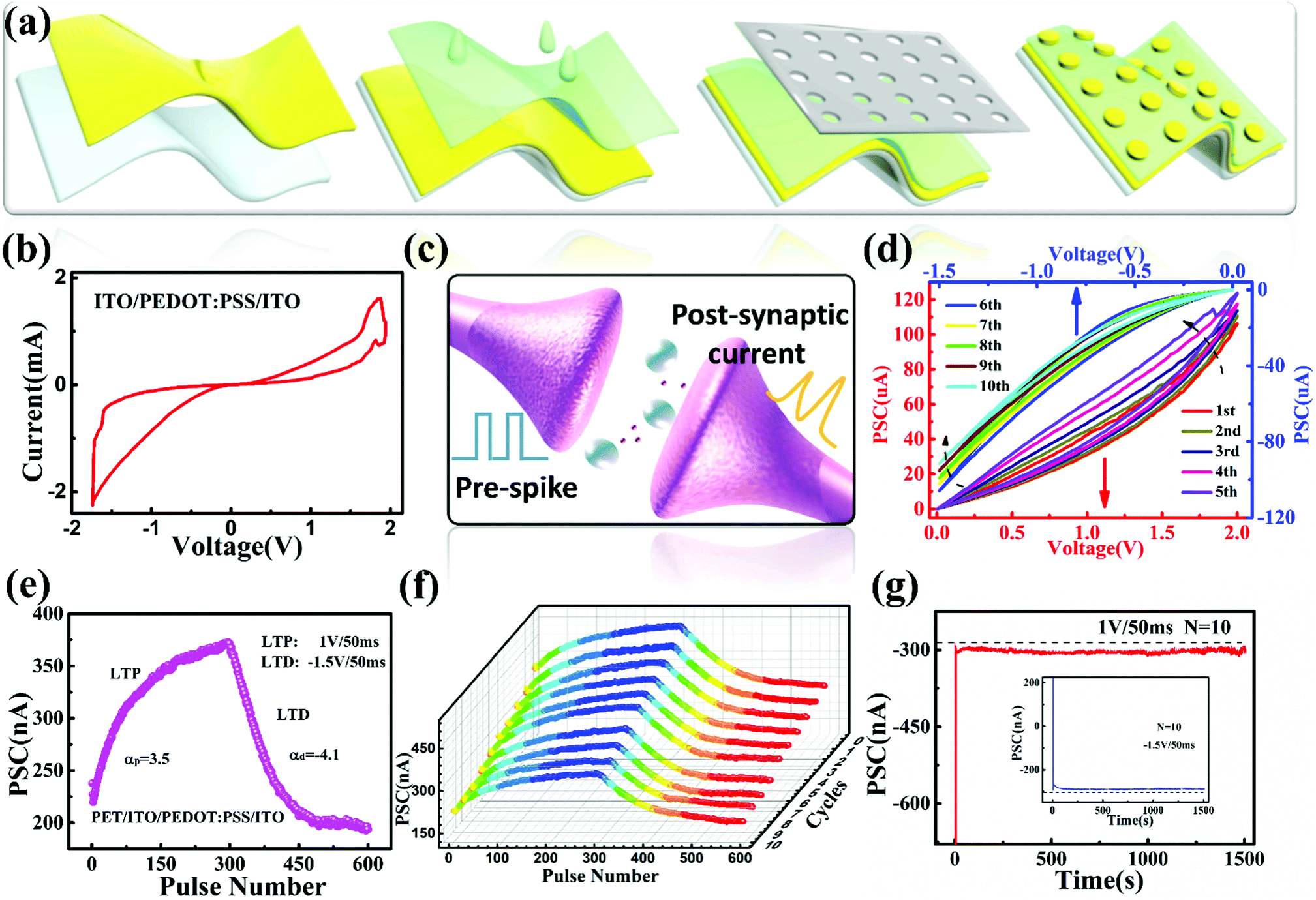
| | Fig. 2 Synaptic plasticity of the PEDOT:PSS-based device. (a) The fabrication process of the flexible artificial synaptic device, which includes spin-coating functional materials (PEDOT:PSS) and sputtering electrodes (ITO) with a hard mask. (b) Nonlinear transmission characteristics of the artificial synapse under a single sweep. (c) Schematic demonstration of a signal transmission between pre- and post-synapses. (d) I–V characteristics with a gradual increase and decrease under successive positive and negative sweeps. (e) LTP and LTD behaviors through a series of potentiating (1 V, 50 ms) and depressing (−1.5 V, 50 ms) pulses. (f) Demonstration of stable LTP/LTD behaviors with 6000 spikes at flat states. (g) Retention characteristics of LTP after 10 positive spikes (1 V, 50 ms). The inset shows retention behaviors of LTD after 10 negative spikes (−1.5 V, 50 ms). | |
Synaptic behaviors of the transparent e-synapse
Typical electrical characteristics of the PEDOT:PSS-based device were demonstrated with a single sweep of DC voltage to the top electrode, while the bottom electrode was grounded (Fig. 2b). The gradual change of current with voltage increase enabled the synaptic measurements. After five cycles of consecutive positive voltage sweeps (0 to 2 V) were applied to the e-synapse, the post-synaptic current showed hysteresis and increased after each loop, while the current level decreased gradually after five negative sweeps (0 to −1.5 V), as shown in Fig. 2d. The artificial synapse is one kind of memristor, which is based on the resistive switching characteristics of devices. It's well known that the common problem of resistive switching memories is the non-uniform distribution of the set/reset voltages. The device in Fig. 2b shows a high current at 1 V in DC mode because the device achieved the set voltage in this cycle and the set process occurred. The current in Fig. 2d at 1 V is lower than that in Fig. 2b, resulting from the facts that the device has not achieved the set voltage in these cycles and the set process did not happen. The gradual modulation characteristics in Fig. 2d were consistent with current characteristics in pulse mode (see Fig. S1 of ESI† for details). The e-synapse was capable of sequentially modulating conductance (i.e. synaptic weight), opening the way for pattern recognition learning function. In biological synapses, synaptic weights play important roles in synaptic strength connection, transferring information, carrying out the commands of neuromorphic systems, and carrying out daily life activities. Action potential from the pre-synapse induced neurotransmitter release and response signals in the post-synapse for signal transmission, as shown in Fig. 2c. Excitatory postsynaptic current (EPSC) and inhibitory postsynaptic current (IPSC) in the e-synapse could be triggered by a single positive or negative electrical pulse (1.5 V/−1.5 V, 10 ms). The postsynaptic current increased or decreased abruptly with pulse application and then relaxed over time after the voltage was removed (see Fig. S2 of ESI† for details).
In order to better simulate the synaptic behavior of LTP/LTD, consecutive pulses (1 V/−1.5 V, 50 ms) were applied to the artificial e-synapse and the post-synaptic current was recorded with a read pulse (0.1 V, 50 ms) after each operation pulse (see Fig. S3 of ESI† for details). The read pulse amplitude was small enough so as not to influence the state of the e-synapse. Fig. 2e shows electrical LTP and LTD, which were the core learning functions in bio-neurons, through repeated operation and read pulses in the developed artificial e-synapse. The nonlinearity coefficient alpha (α) is one of the important parameters to describe the weights update in a synaptic device. As shown in Fig. S4 of the ESI,† the parameters of device in potentiation (αp) and depression (αd) are extracted by fitting the weights update curve, where αp = 3.5 and αd = −4.1.47–49 Based on the typical synaptic weights update behavior and power formula ![[W with combining macron]](https://www.rsc.org/images/entities/i_char_0057_0304.gif) = (V2 × ΔG × t)/Npulse, the average energy consumption of PEDOT:PSS-based devices during the training process in LTP and LTD is 252.7 pJ per spike and 666.7 pJ per spike. The conductance modulation in LTP could be attributed to the formation and strength of the conductive filament PEDOT+. By applying a positive stimulus to the ITO top electrode, PEDOT0 transformed into PEDOT+ by hole injection, and PEDOT+ from the bottom electrode accumulated on the top electrode, which caused an increase in the conductance of the device (see Fig. S5 of ESI†). In contrast, the conductance of the device gradually decreased under identical negative pulses due to hole extraction and because PEDOT+ changed into non-conductive PEDOT0, resulting in the rupture of conductive paths.44,50
= (V2 × ΔG × t)/Npulse, the average energy consumption of PEDOT:PSS-based devices during the training process in LTP and LTD is 252.7 pJ per spike and 666.7 pJ per spike. The conductance modulation in LTP could be attributed to the formation and strength of the conductive filament PEDOT+. By applying a positive stimulus to the ITO top electrode, PEDOT0 transformed into PEDOT+ by hole injection, and PEDOT+ from the bottom electrode accumulated on the top electrode, which caused an increase in the conductance of the device (see Fig. S5 of ESI†). In contrast, the conductance of the device gradually decreased under identical negative pulses due to hole extraction and because PEDOT+ changed into non-conductive PEDOT0, resulting in the rupture of conductive paths.44,50
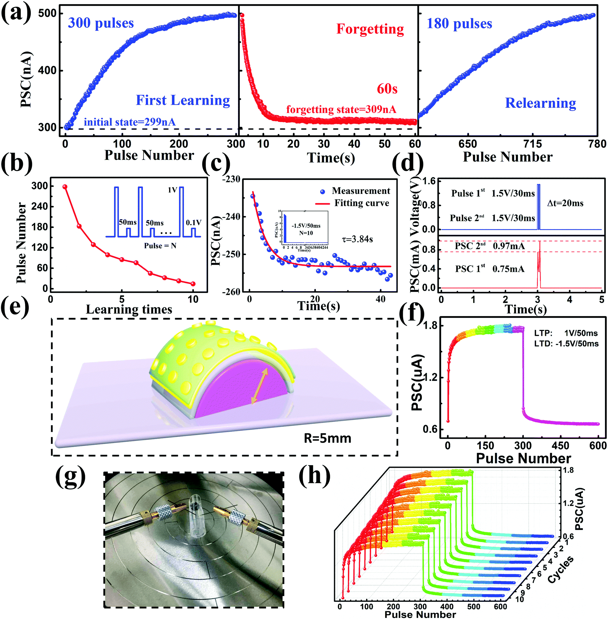
Over 300 conductance states were demonstrated, indicating that multiple weights of the e-synapse were available for weights update in the training and learning process of pattern recognition. A reproducible stable spike-current response can be seen in Fig. 2f. In order to verify the endurance of the e-synapse, 6000 pulses were applied to the top electrode. In neuromorphic computing systems, non-volatility is the basis of learning and memory function in an e-synapse. The conductance state could hold for over 1500 s in both LTP and LTD after 10 pre-spikes (1 V/−1.5 V, 50 ms) at a read bias of 0.1 V, showing a non-volatile memory potential (Fig. 2g). In the brain, receiving new information would go through the process of learning, forgetting, and relearning. The relearning process makes the recovery of forgotten knowledge easier than learning for the first time.51 The phenomenon was observed in the developed transparent e-synapse (Fig. 3a). The initial PSC is 299 nA. After 300 successive bias pulses were applied to the device, a spontaneous decay of the synaptic weight in the e-synapse occurred. When the intermediate state became stable (309 nA), 180 pulses were sufficient for the device to recover to the synaptic weights level as in the first learning process. As can be observed in Fig. S6 of the ESI,† in order to achieve the same memory capability, different numbers of pulses were used under different relearning cycles. It should be noted that the 10th forgetting state achieved 456 nA, indicating the learning-experience behavior in our artificial synaptic device (see Fig. S7 of ESI†). With the increase of relearning cycles, the pulses needed for achieving the same weights level decreased. After repeating the relearning process for 10 cycles, it took only 15 pulses for the device to recover the memory level (Fig. 3b).
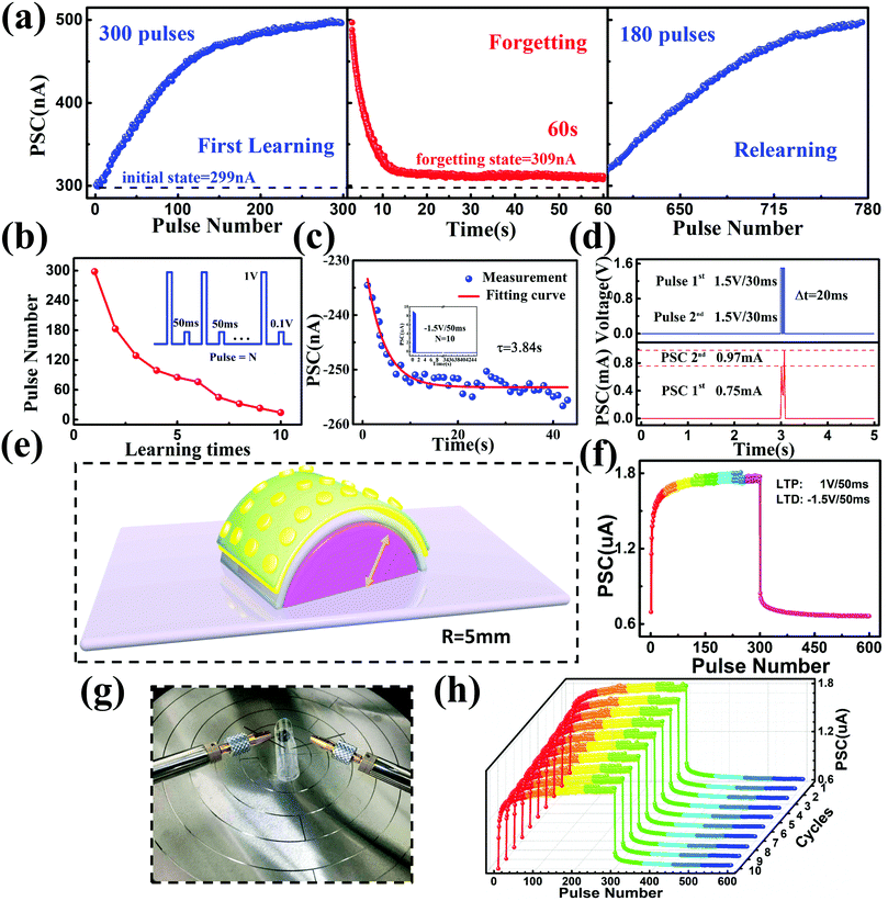 |
| | Fig. 3 Synaptic behaviors under bent states. (a) Learning behaviors of the synaptic device, containing learning, forgetting, and relearning processes. The initial PSC is 299 nA and the 1st forgetting state of the device is 309 nA after a 60 s forgetting process. (b) Pulse number decreases with the increase of learning cycles. The inset shows operating and reading pulses during the learning process. (c) Forgetting curve after 10 negative spikes (−1.5 V, 50 ms). The inset shows the instant current response during the spikes applied to the device. (d) Emulation of PPF behavior using a pair of potentiating pre-spikes (1.5 V, 30 ms) with a 20 ms interval. (e) Schematic diagram of the flexible artificial synapse under a bending radius of 5 mm. (f) Mimicking of LTP/LTD behavior when the fabricated flexible device is at a bending state. (g) Image of the device under bent conditions during electrical measurements. (h) Cycling reliability tests (10 cycles) on the bent device with 6000 spikes (1 V/−1.5 V, 50 ms). | |
During the forgetting process, the synaptic weight gradually dropped to the stabilized state, which expressed the information storage capability after the learning process. The forgetting curve was fitted and analyzed by the modified Kohlrausch law, widely used in psychology and recently in e-synapses1,52
| | I(t) = I0 + A![[thin space (1/6-em)]](https://www.rsc.org/images/entities/char_2009.gif) exp(−t/τ) exp(−t/τ) | (1) |
where
I(
t) and
I0 are the instant current at time
t and the stabilized current after the decay, respectively.
A and
τ are the pre-factor and relaxation time constants for the evaluation of the forgetting rate, respectively. In
Fig. 3c, it can be seen that the forgetting behavior of the e-synapse occurred after 10 negative spikes and the relaxation constant
τ was 3.84 s. In addition to long-term plasticity, short-term plasticity (STP) also played an important role in the bio-synapse. As one of the typical STP characteristics, PPF occurred when the second pulse-induced EPSC was larger than the first output signal, which was determined by the time interval between two paired pulses. The transparent e-synapse exhibited a PPF behavior with two pulses (1.5 V/30 ms) with a 20 ms interval (
Fig. 3d). The power consumption of the synaptic device could be reduced in several ways, including fabricating devices with a smaller size, and applying pulses with a shorter width and smaller pulse amplitude.
Mechanical flexibility of the e-synapse
In order to demonstrate the synaptic plasticity of the flexible artificial synapse, the LTP and LTD behaviors were simulated. The flexibility of the e-synapse was measured with a bending radius of 5 mm (Fig. 3e). Consecutive pulses (1 V/−1.5 V, 50 ms) were applied to the top electrode while the bottom electrode was grounded (Fig. 3g). The e-synapse showed excellent electrical synaptic plasticity at the bent state (Fig. 3f). The electrical characteristics in LTP and LTD behaviors were similar to the flat state performance characteristics. In order to further verify the reliability of mechanical flexibility, 6000 spikes were repeatedly applied so as to achieve reproducible and consistent performance of the e-synapse (Fig. 3h). Stable LTP/LTD indicated excellent flexibility of the developed e-synapse.
Pattern recognition based on a neuromorphic network
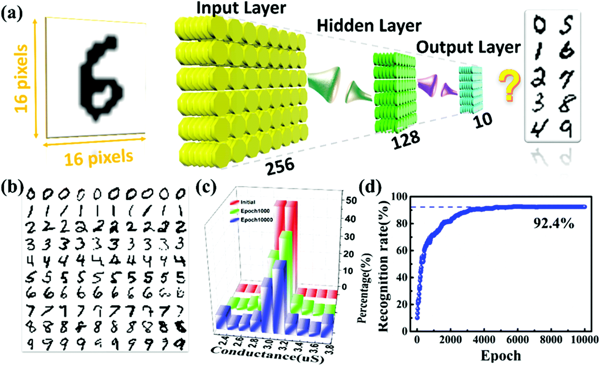
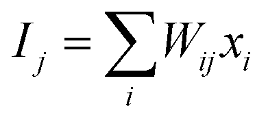
In order to investigate the applicability of artificial intelligence in pattern recognition, a three-layer neural network system was constructed based on the developed transparent, flexible, and biocompatible e-synapse with LTP/LTD behaviors. The system consisted of an input layer, a hidden layer, and an output layer, which were connected with 256 × 128 and 128 × 10 e-synapses (Fig. 4a). The images used in pattern recognition were pre-processed and rescaled to 16 × 16 pixels in order to match the 256 input neurons. There were 10000 initial samples used for training the multilayer perceptron network based on backpropagation, while 500 samples were used to verify the recognition effect. Fig. 4b shows an example of 100 handwritten digits from “0” to “9”, randomly taken from the MNIST database for training. The training process was based on a back propagation algorithm (see Fig. S8 of ESI†). The training images were applied as the input signal of the 1st layer neurons and the calculated result  was used as the input of the hidden layer. After the activation process using a log-sigmoid (logsig) function, the output signal of
  in the 3rd layer neurons was determined. Next, the altering values of synaptic weights ΔWij and ΔWjk for weights update were calculated by comparing the real output and target output, and with one epoch of training process finished. Based on the above simulation, the digits from “0” to “9” could be well classified.
 |
| | Fig. 4 Pattern recognition by the fabricated neural network. (a) Artificial neural network for handwritten digit recognition, containing an input layer (256 neurons), a hidden layer (128 neurons), and an output layer (10 neurons). The digit “6” was recalled, consisting of 16 × 16 pixels. (b) Example of the rescaled MNIST images. “0–9” digits were used for training. (c) Synaptic weights change during the training process, at the initial, the 1000th, and the 10000th epoch. (d) Classification rate as a function of training epoch. After 5000 epochs, the recognition rate reached 92.4%. | |
The output signals of the training and testing images containing “0” to “9” digits during the training and verifying processes can be seen in Fig. S9 of the ESI.† The neural network constructed by the developed synaptic devices was able to identify the digit “0” from other training digits after 2000 epochs, while it was able to select the digit “0” from other verifying digits after 1500 epochs. The results indicated that 2000 epochs were enough to recognize the digit “0” for the training artificial neural network. However, a simulated recognition accuracy of 92.4% could be achieved after 4000 training epochs and it remained stable (Fig. 4d). The different number of epochs needed for stable recognition was due to the influence of the other digits (“1” to “9”). In order to verify that the selected hidden layer (128 neurons) was appropriate for this work, neural networks with 64, 256, and 512 neurons in the hidden layer were also simulated (see Fig. S10 of ESI†). The comparative results further proved that the artificial system with 128 neurons in the hidden layer was suitable for applications in pattern recognition. In the initial synaptic devices, the conductance that connected the different layers was in the range of 2.94–3.1 μS. After 10000 training epochs, the final weights covered a range of 2.3–3.74 μS. Compared to the concentrated distribution of the initial conductance, the distribution of the synaptic weights of all the e-synapses became uniform after training (Fig. 4c). The neural network exhibited a reliable recognition function based on the developed transparent, flexible, and biocompatible artificial synapses.
Artificial synapses for organic environments
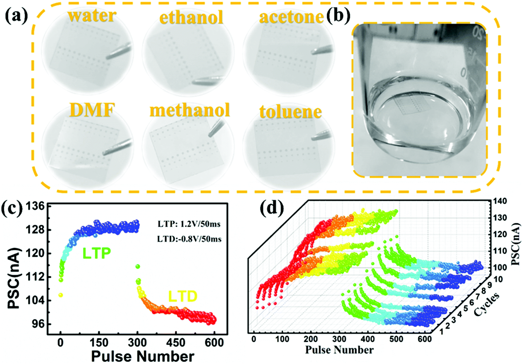
It is hard for organic devices to remain stable, due to the fact that the organic functional layer may be dissolved and unable to function after contacting water and/or organic solvents. This disadvantage makes the widespread use of organic devices challenging. However, the compatible organic e-synapse developed in the present study was able to avoid damage from water and the most common organic solvents. As can be seen in Fig. 5b, the device was immersed in water for over 12 hours and no decomposition was observed. Additionally, the device was also immersed in ethanol, acetone, DMF, methanol, and toluene for over 60 hours in total (see Fig. S11 of ESI†). The artificial synaptic electronic device can be seen in Fig. 5a. The structure of the device could be clearly observed and the film showed no trace of dissolution. In order to confirm the normal function of the synaptic device after the water and organic solvent treatments, successive pulses were applied to the top electrode. The typical bio-synaptic plasticity (i.e., LTP/LTD) was successfully emulated with positive spikes of 1.2 V and negative spikes of −0.8 V (Fig. 5c). The reproducible long-term plasticity of the artificial synapses was also demonstrated with 6000 spikes, which proved that the specific device was able to avoid short period damage in organic environments (Fig. 5d).
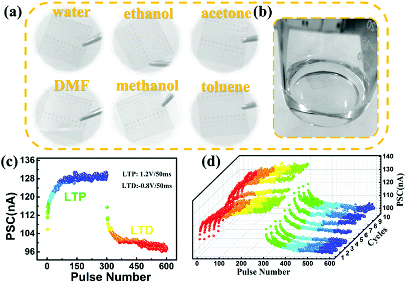 |
| | Fig. 5 Demonstration of the synaptic behavior of the fabricated device for organic environments. (a) Images of the intact device after immersing in water, ethanol, acetone, DMF, methanol, and toluene. The water and organic solvent resistance tests lasted for over 72 hours. (b) The organic environment test. The entire artificial synaptic device was immersed in water for over 12 hours. (c) Potentiation and depression behavior of the device based on potentiating (1.2 V, 50 ms) and depressing (−0.8 V, 50 ms) spikes after immersion in six different solvents. (d) Stable long-term potentiation and depression of the artificial synaptic device for 10 cycles after treatment in organic environments. | |
Conclusions
In summary, a transparent, flexible, and biocompatible organic artificial synaptic device for organic environments was developed, paving the way for applications in pattern recognition. Compared with recent reports on synaptic devices (Table 1), our device showed great performance in flexibility, transparency, biocompatibility, pattern recognition and resisting organic environments. With the simple ITO/PEDOT:PSS/ITO structure, the device demonstrated an excellent transparency of 87.5% at 550 nm wavelength and flexibility at a radius of 5 mm. Typical synaptic plasticity characteristics, including EPSC/IPSC, PPF, and learning–forgetting–relearning processes, were emulated. Furthermore, the e-synapse exhibited reliable LTP/LTD behaviors at the flat and bent states, even after being immersed in water and organic solvents for over 12 hours. The neural network of e-synapses achieved a 92.4% handwritten digit recognition accuracy, paving the way for reliable artificial neuromorphic computing systems.
Table 1 Comparison of the parameters and functions of several kinds of artificial synaptic devices
| Materials system |
Flexible |
Biocompatibility |
Organic environment |
Pattern recognition |
Transmittance [%] |
Modulated states |
Ref. |
|
Ag nanoparticle-doped thermoplastic polyurethanes.
Poly(2-vinylnaphthalene).
p-Channel poly[4-(4,4-dihexadecyl-4H-cyclopenta[1,2-b:5,4-b]dithiophen-2-yl)-alt[1,2,5]thiadiazolo[3,4-c]-pyridine] (PCDTPT) and keratin dielectric thin-film transistors.
|
| Pt/ZHO/TiN |
— |
— |
— |
Yes |
— |
10 |
53
|
| Au/TPU:Ag NPs/Aua |
Yes |
Yes |
— |
— |
— |
15 |
39
|
| IGZO/Al2O3/Ta2O5−x/Ta |
Yes |
— |
— |
— |
— |
30 |
54
|
| ITO/lignin/Au |
Yes |
Yes |
— |
— |
— |
50 |
1
|
| Pentacene/PVNb transistor |
— |
Yes |
— |
— |
— |
100 |
55
|
| CNT transistor |
Yes |
Yes |
— |
Yes |
— |
120 |
56
|
| FTO/ZnO/In2O3 |
— |
— |
— |
— |
76% |
10 |
12
|
| PCDTPT/keratin TFTsc |
Yes |
Yes |
— |
— |
∼80% |
— |
57
|
| ITO/collagen/Mg |
Yes |
Yes |
— |
— |
∼85% |
200 |
4
|
| This work |
Yes |
Yes |
Yes |
Yes |
87.5% |
300 |
This work |
Experimental
Device fabrication process
The artificial synaptic devices with a transparent structure were prepared on a poly(ethylene terephthalate) (PET) substrate, which was purchased from Sigma-Aldrich. The substrate was cleaned using acetone, isopropanol, and deionized water for 5 minutes, followed by nitrogen. Prior to spin-coating, the solution of PEDOT:PSS (CLEVIOS PH1000) was filtered through filters with 0.22 μm pore size. The filtered solution was spin-coated at 500 rpm for 5 s and 4000 rpm for 1 min followed by baking at 120 °C on a hot plate for 15 min. Subsequently, a functional layer with a thickness of 42.18 nm was formed. ITO top electrodes with a diameter of 200 μm were patterned by sputtering.
Characterization
Top view and cross-sectional images of the active layers were taken with a ZEISS SIGMA HD scanning electron microscope. The topography image of the organic film was obtained by atomic force microscopy (AFM) based on tapping mode. The transmission spectra of the device in the range of 300–800 nm were observed using a PerkinElmer Lambda 750S Spectrometer. In order to analyze the chemical structure of PEDOT:PSS, Raman spectra were collected using a LabRAM XploRA Raman spectrometer (Horiba Jobin Yvon, France) with a wavelength of 532 nm. The electrical characteristics were measured using a semiconductor parameter analyzer (Agilent B1500A) with an Agilent B1525 Pulse Generator Unit under flat and bent states. During electrical measurements, voltage was applied on the top ITO electrode while the bottom ITO electrode was grounded.
Conflicts of interest
There are no conflicts to declare.
Acknowledgements
We acknowledge the use of the MINST digit Database. This work was supported by the NSFC (61704030 and 61522404), Shanghai Rising-Star Program (19QA1400600), the Program of Shanghai Subject Chief Scientist (18XD1402800), and the Support Plans for the Youth Top-Notch Talents of China.
References
- Y. Park and J. Lee, ACS Nano, 2017, 11, 8962–8969 CrossRef CAS PubMed.
- C. Wu, T. W. Kim, H. Y. Choi, D. B. Strukov and J. J. Yang, Nat. Commun., 2017, 8, 752 CrossRef PubMed.
- P. A. Merolla, J. V. Arthur, R. Alvarez-Icaza, A. S. Cassidy, J. Sawada, F. Akopyan, B. L. Jackson, N. Imam, C. Guo, Y. Nakamura, B. Brezzo, I. Vo, S. K. Esser, R. Appuswamy, B. Taba, A. Amir, M. D. Flickner, W. P. Risk, R. Manohar and D. S. Modha, Science, 2014, 345, 668 CrossRef CAS PubMed.
- N. Raeis-Hosseini, Y. Park and J. Lee, Adv. Funct. Mater., 2018, 28, 1800553 CrossRef.
- H. Wang, Q. Zhao, Z. Ni, Q. Li, H. Liu, Y. Yang, L. Wang, Y. Ran, Y. Guo, W. Hu and Y. Liu, Adv. Mater., 2018, 30, 1803961 CrossRef PubMed.
- J. T. Yang, C. Ge, J. Y. Du, H. Y. Huang, M. He, C. Wang, H. B. Lu, G. Z. Yang and K. J. Jin, Adv. Mater., 2018, 30, 1801548 CrossRef PubMed.
- D. Silver, A. Huang, C. J. Maddison, A. Guez, L. Sifre, G. van den Driessche, J. Schrittwieser, I. Antonoglou, V. Panneershelvam, M. Lanctot, S. Dieleman, D. Grewe, J. Nham, N. Kalchbrenner, I. Sutskever, T. Lillicrap, M. Leach, K. Kavukcuoglu, T. Graepel and D. Hassabis, Nature, 2016, 529, 484 CrossRef CAS PubMed.
- K. Bong, S. Choi, C. Kim and H. Yoo, IEEE Micro, 2017, 37, 30–38 Search PubMed.
- K. L. Kim, W. Lee, S. K. Hwang, S. H. Joo, S. M. Cho, G. Song, S. H. Cho, B. Jeong, I. Hwang, J. Ahn, Y. Yu, T. J. Shin, S. K. Kwak, S. J. Kang and C. Park, Nano Lett., 2016, 16, 334–340 CrossRef CAS PubMed.
- Z. Zheng, L. Gan, H. Li, Y. Ma, Y. Bando, D. Golberg and T. Zhai, Adv. Funct. Mater., 2015, 25, 5885–5894 CrossRef CAS.
- X. Yan, Z. Zhou, J. Zhao, Q. Liu, H. Wang, G. Yuan and J. Chen, Nano Res., 2018, 11, 1183–1192 CrossRef CAS.
- M. Kumar, S. Abbas and J. Kim, ACS Appl. Mater. Interfaces, 2018, 10, 34370–34376 CrossRef CAS PubMed.
- S. Hwang, G. Park, H. Cheng, J. Song, S. Kang, L. Yin, J. Kim, F. G. Omenetto, Y. Huang, K. Lee and J. A. Rogers, Adv. Mater., 2014, 26, 1992–2000 CrossRef CAS PubMed.
- J. Yoon, Y. Ji, S. Lee, J. Hyon and J. M. Tour, Adv. Electron. Mater., 2018, 4, 1700665 CrossRef.
- K. A. S. C. Ali, Nanotechnology, 2017, 28, 25303 CrossRef PubMed.
- H. E. Lee, J. H. Park, T. J. Kim, D. Im, J. H. Shin, D. H. Kim, B. Mohammad, I. Kang and K. J. Lee, Adv. Funct. Mater., 2018, 28, 1801690 CrossRef.
- G. Zhang, T. Guo, X. He, Z. Ai, H. Wu and C. Liu, Adv. Electron. Mater., 2018, 4, 1800195 CrossRef.
- J. Shang, W. Xue, Z. Ji, G. Liu, X. Niu, X. Yi, L. Pan, Q. Zhan, X. Xu and R. Li, Nanoscale, 2017, 9, 7037–7046 RSC.
- C. H. Ho, J. R. D. Retamal, P. K. Yang, C. P. Lee, M. L. Tsai, C. F. Kang and J. He, Sci. Rep., 2017, 7, 44429 CrossRef CAS PubMed.
- Y. H. Liu, L. Q. Zhu, P. Feng, Y. Shi and Q. Wan, Adv. Mater., 2015, 27, 5599–5604 CrossRef CAS PubMed.
- Y. Wang, Z. Lv, J. Chen, Z. Wang, Y. Zhou, L. Zhou, X. Chen and S. Han, Adv. Mater., 2018, 30, 1802883 CrossRef PubMed.
- X. Chen, J. Pan, J. Fu, X. Zhu, C. Zhang, L. Zhou, Y. Wang, Z. Lv, Y. Zhou and S. Han, Adv. Electron. Mater., 2018, 4, 1800444 CrossRef.
- J. Kim, J. H. Lee, H. Ryu, J. Lee, U. Khan, H. Kim, S. S. Kwak and S. Kim, Adv. Funct. Mater., 2017, 27, 1700702 CrossRef.
- M. Lübben, P. Karakolis, V. Ioannou-Sougleridis, P. Normand, P. Dimitrakis and I. Valov, Adv. Mater., 2015, 27, 6202–6207 CrossRef PubMed.
- X. Liao, Z. Zhang, Q. Liang, Q. Liao and Y. Zhang, ACS Appl. Mater. Interfaces, 2017, 9, 4151–4158 CrossRef CAS PubMed.
- G. Wang and H. Chen, Sep. Purif. Technol., 2013, 120, 402–409 CrossRef CAS.
- L. Wang, S. Yang, J. Wang, C. Wang and L. Chen, Mater. Lett., 2011, 65, 869–872 CrossRef CAS.
- Z. He, J. Chen, Z. Sun, G. Szulczewski and D. Li, Org. Electron., 2012, 13, 1819–1826 CrossRef CAS.
- E. Stavrinidou, R. Gabrielsson, E. Gomez, X. Crispin, O. Nilsson, D. T. Simon and M. Berggren, Sci. Adv., 2015, 1, e1501136 CrossRef PubMed.
- Y. van de Burgt, E. Lubberman, E. J. Fuller, S. T. Keene, G. C. Faria, S. Agarwal, M. J. Marinella, A. Alec Talin and A. Salleo, Nat. Mater., 2017, 16, 414 CrossRef CAS PubMed.
- A. G. Ricciardulli, S. Yang, G. A. H. Wetzelaer, X. Feng and P. W. M. Blom, Adv. Funct. Mater., 2018, 28, 1706010 CrossRef.
- J. Choi, J. S. Han, K. Hong, S. Y. Kim and H. W. Jang, Adv. Mater., 2018, 30, 1704002 CrossRef PubMed.
- L. Hu, M. Li, K. Yang, Z. Xiong, B. Yang, M. Wang, X. Tang, Z. Zang, X. Liu, B. Li, Z. Xiao, S. Lu, H. Gong, J. Ouyang and K. Sun, J. Mater. Chem. A, 2018, 6, 16583–16589 RSC.
- Y. Zheng, J. Yu, J. Tang, F. Yang, C. Wang, B. Wei and X. Li, Org. Electron., 2018, 62, 491–498 CrossRef CAS.
- C. M. Palumbiny, F. Liu, T. P. Russell, A. Hexemer, C. Wang and P. Müller-Buschbaum, Adv. Mater., 2015, 27, 3391–3397 CrossRef CAS PubMed.
- R. C. Froemke, M. M. Merzenich and C. E. Schreiner, Nature, 2007, 450, 425 CrossRef CAS PubMed.
- Z. Wang, S. Joshi, S. E. Savel Ev, H. Jiang, R. Midya, P. Lin, M. Hu, N. Ge, J. P. Strachan, Z. Li, Q. Wu, M. Barnell, G. Li, H. L. Xin, R. S. Williams, Q. Xia and J. J. Yang, Nat. Mater., 2016, 16, 101 CrossRef PubMed.
- A. C. Penn, C. L. Zhang, F. Georges, L. Royer, C. Breillat, E. Hosy, J. D. Petersen, Y. Humeau and D. Choquet, Nature, 2017, 549, 384 CrossRef CAS PubMed.
- M. Yang, X. Zhao, Q. Tang, N. Cui, Z. Wang, Y. Tong and Y. Liu, Nanoscale, 2018, 10, 18135–18144 RSC.
- M. Morales-Masis, S. De Wolf, R. Woods-Robinson, J. W. Ager and C. Ballif, Adv. Electron. Mater., 2017, 3, 1600529 CrossRef.
- M. Kumar, H. Kim, D. Y. Park, M. S. Jeong and J. Kim, ACS Appl. Mater. Interfaces, 2018, 10, 12768–12772 CrossRef CAS PubMed.
- S. Ju, A. Facchetti, Y. Xuan, J. Liu, F. Ishikawa, P. Ye, C. Zhou, T. J. Marks and D. B. Janes, Nat. Nanotechnol., 2007, 2, 378 CrossRef CAS PubMed.
- X. Wu, Y. Chu, R. Liu, H. E. Katz and J. Huang, Advanced Science, 2017, 4, 1700442 CrossRef PubMed.
- P. J. Chia, L. L. Chua, S. Sivaramakrishnan, J. M. Zhuo, L. H. Zhao, W. S. Sim, Y. C. Yeo and P. K. Ho, Adv. Mater., 2007, 19, 4202–4207 CrossRef CAS.
- S. Garreau, G. Louarn, J. P. Buisson, G. Froyer and S. Lefrant, Macromolecules, 1999, 32, 6807–6812 CrossRef CAS.
- C. Zhou, Z. Liu, X. Du and S. P. Ringer, Synth. Methods, 2010, 160, 1636–1641 CrossRef CAS.
- M. Jerry, P. Chen, J. Zhang, P. Sharma, K. Ni, S. Yu and S. Datta, Int. Electron Devices Meet., 2017, 2–6 Search PubMed.
- W. Chung, M. Si and D. Y. Peide, Int. Electron Devices Meet., 2018, 12–15 Search PubMed.
- S. Yu, P. Chen, Y. Cao, L. Xia, Y. Wang and H. Wu, Int. Electron Devices Meet., 2015, 13–17 CAS.
- T. Wang, Z. He, H. Liu, L. Chen, H. Zhu, Q. Sun, S. Ding, P. Zhou and D. W. Zhang, ACS Appl. Mater. Interfaces, 2018, 10, 37345–37352 CrossRef CAS PubMed.
- G. Liu, C. Wang, W. Zhang, L. Pan, C. Zhang, X. Yang, F. Fan, Y. Chen and R. Li, Adv. Electron. Mater., 2015, 2, 1500298 CrossRef.
- T. Chang, S. Jo and W. Lu, ACS Nano, 2011, 5, 7669–7676 CrossRef CAS PubMed.
- L. Chen, T. Wang, Y. Dai, M. Cha, H. Zhu, Q. Sun, S. Ding, P. Zhou, L. Chua and D. W. Zhang, Nanoscale, 2018, 10, 15826–15833 RSC.
- X. Yan, J. Wang, M. Zhao, X. Li, H. Wang, L. Zhang, C. Lu and D. Ren, Appl. Phys. Lett., 2018, 113, 13503 CrossRef.
- Y. Zhong, T. Wang, X. Gao, J. Xu and S. Wang, Adv. Funct. Mater., 2018, 28, 1800854 CrossRef.
- S. Kim, B. Choi, M. Lim, J. Yoon, J. Lee, H. Kim and S. Choi, ACS Nano, 2017, 11, 2814–2822 CrossRef CAS PubMed.
- J. Ko, L. T. H. Nguyen, A. Surendran, B. Y. Tan, K. W. Ng and W. L. Leong, ACS Appl. Mater. Interfaces, 2017, 9, 43004–43012 CrossRef CAS PubMed.
Footnote |
| † Electronic supplementary information (ESI) available. See DOI: 10.1039/c9nh00341j |
|
| This journal is © The Royal Society of Chemistry 2019 |
Click here to see how this site uses Cookies. View our privacy policy here. 
 *,
Hao
Zhu
,
Qing-Qing
Sun
*,
Shi-Jin
Ding
*,
Hao
Zhu
,
Qing-Qing
Sun
*,
Shi-Jin
Ding
 was used as the input of the hidden layer. After the activation process using a log-sigmoid (logsig) function, the output signal of
 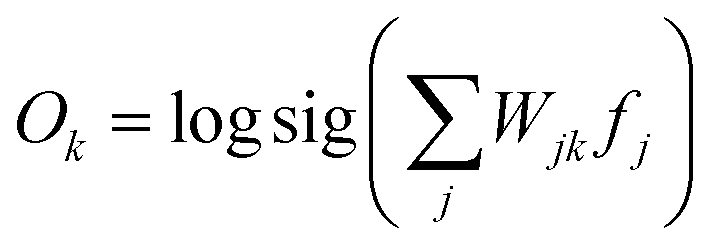 in the 3rd layer neurons was determined. Next, the altering values of synaptic weights ΔWij and ΔWjk for weights update were calculated by comparing the real output and target output, and with one epoch of training process finished. Based on the above simulation, the digits from “0” to “9” could be well classified.