Room-temperature bonding of glass chips via PTFE-assisted plasma modification for nanofluidic applications†
Qiushi
Kang
a,
Chenxi
Wang
 *a,
Kaimeng
Liu
a and
Takehiko
Kitamori
 b
b
aState Key Laboratory of Advanced Welding and Joining, Harbin Institute of Technology, Harbin 150001, China. E-mail: wangchenxi@hit.edu.cn
bCollaborative Research Organization for Micro and Nano Multifunctional Devices, The University of Tokyo, 7-3-1 Hongo, Bunkyo, Tokyo 113-8656, Japan
First published on 15th May 2023
Abstract
Fused-silica glass, as a desirable material with rigidity, biological inertness, and favorable light transmission for nanofluidic devices, should be assembled via low-temperature bonding technology to hermetically seal channels for stable liquid manipulation in extended-nano (101–103 nm) space. Confronted with the predicament of localized functionalization of nanofluidic applications (e.g. DNA microarray) with temperature-sensitive structures, the room-temperature direct bonding of glass chips to achieve modification of channels prior to bonding offers a considerably attractive solution to avoid component denaturation during the conventional post-bonding heating process. Therefore, we developed a nano-structure friendly and technically convenient room-temperature (RT, 25 °C) glass–glass direct bonding technology using polytetrafluoroethylene (PTFE)-assisted plasma modification without a requirement for special equipment. Unlike the establishment of chemical functionalities relying on immersion in potent but dangerous chemicals like HF, the fluorine radicals (F*) from PTFE pieces with superior chemical inertness were introduced on glass surfaces via O2 plasma sputtering and constructed fluorinated silicon oxides on the glass surfaces effectively, eliminating the significant etching effect of HF to protect fine nanostructures. Very strong bonding was obtained at RT with no heating and the high-pressure resistant glass–glass interfaces were evaluated under high-pressure-driven flow conditions up to 2 MPa based on a two-channel liquid introduction system. Moreover, the favorable optical transmittance of the fluorinated bonding interface demonstrated a capacity for high-resolution optical detection or liquid sensing.
1. Introduction
The concept of lab-on-a-chip aims to integrate the capability of a laboratory into a miniaturized nanofluidic system for rapid and accurate detection at the chip scale which is close to commercial reality. Owing to the manipulation of liquid-containing reagents at an extended nanoscale (typically 101–103 nm) to control reactions, nanofluidics has attracted much attention for its promising applications using its dominant surface effect and extremely small volume, spanning disease monitoring and management, chemical synthesis, biomedical tissue engineering, and environmental sampling.1–5 Compared with well-established polymer substrates (e.g. polydimethylsiloxane, PDMS) with low stiffness and water permeability, fused-silica glass substrates are extensively used for nanofluidic devices because they offer overwhelming advantages including chemical inertness, higher values of Young's modulus and light transmission, and can be used to fabricate nanostructures with high resolution and avoid fluid leaching and evaporation.6,7 To achieve nanofluidic devices successfully, it is paramount to construct and hermetically seal channels via assembling glass substrates with nanostructures. To date, low-temperature bonding has provided a desirable assembly solution with the merits of protecting high-temperature sensitive functional components immobilized in channels such as biomolecules, electrodes, sensors, waveguides, optical components, etc.8 Adhesive bonding (intermediate-layer bonding), as an important bonding technology performed at low temperatures, can integrate polymer, semiconductor, metal, and ceramic substrates by introducing micron-thick thermal or photo-curable resin at the interface. Seamless, void-free robust glass bonding interfaces have been obtained through PDMS,9,10 SU-8,11 and benzocyclobutene (BCB)12,13 within 300 °C. However, the dispensing of adhesive resin has potential for channel contamination and clogging, and adhesive bonds are not stable enough for long-term service due to the chemical reactivity of resins.As a clogging-free solution for nanofluidic applications, a direct bonding approach flourishes, relying on low-temperature chemical reactions between functionalized surfaces to achieve covalent bonds eventually, also known as “chemical gluing”.14 Rather than the use of micron-scale resins, liquid chemical “glues” (e.g., 3-aminopropyl trimethoxysilane, APTES) as crosslinking agents can establish a nanometer-scale self-assembled monolayer (SAM) on the surface through several-hours immersion, reducing the risk of channel clogging and interfacial instability.15,16 It has been reported that C–C or Si–O–Si bonds can be achieved at 150–200 °C between hydroxylated, aminosilylated, or carboxylated glass surfaces according to reactions like the Diels–Alder cycloaddition reaction.17–19 With ultra-high surface-area-to-volume ratios and ultrashort diffusion lengths, the sealed nanochannels provide a remarkable arena for affinity-based recognition events such as immunoassays or DNA analysis. However, in the case of direct bonding at low temperatures, the immobilization of temperature-sensitive biomolecules should be performed after the bonding process to protect from any possible denaturation (e.g. proteins denature at temperatures above 40 °C (ref. 20)). The DNA microarray technique has flourished over the past few years since the partial modifications of nanochannels with DNA ligands with functionality and specificity enable more data to be collected than single-point experiments.21 In this occasion, however, the bottleneck lies in the formation of covalent bonds at predetermined spots to immobilize different ligands only to portions of the channel, which is difficult to achieve after bonding due to the limited extended nanospace. In order to solve this technical issue, the room-temperature direct bonding of glass chips to realize partial functionalization of channels prior to bonding offers a considerably attractive solution.
To date, the realization of room-temperature bonding essentially relied on surface modification via dry or wet approaches. Regarding surface dry activation, wafer-level glass–glass bonding was achieved at room temperature successfully via reactive ion etching (RIE) O2 plasma followed by N2 radical microwave (MW) plasma activation in the same chamber (so-called sequential plasma activation).22 Similarly, Takeuchi and co-workers obtained a glass–glass interface with a bonding energy of 1.32 J m−2 by means of Ar ion bombardment under ultrahigh vacuum (<10−5 Pa) conditions, cooperating with in situ AlO film deposition on the glass surfaces.23 However, owing to the necessity for special activation equipment, the productivity of nanofluidic applications based on the above methods has been greatly limited. In contrast, room-temperature bonding based on surface wet chemical cleaning broke the dilemma about special equipment. For instance, glass–glass interfaces could be attained through room-temperature treatment with sulfuric acid (H2SO4),24 hydrofluoric acid (HF),25 or hydrogen fluoride steam.26 Nevertheless, the extensive utilization of dangerous chemicals was not conducive to establishing a toxic-free environment and should be avoided for non-essential societal use. Furthermore, the essence of HF activation lies in the sufficient SiO2 etching rate (10 nm min−1) based on the chemical reaction (SiO2 + 4HF → SiF4↑ + 2H2O), which could destroy the fine nanostructures in the devices.25 Recently, a water-droplet bonding method was developed to realize room-temperature glass bonding via H2O as the bonding agent.6 A pressure endurance of more than 600 kPa within 6 h of bonding was sufficient for cell cultivation, but far from suitable for high-pressure nanofluidic scenarios. Overall, these methods are not cost-effective, nano-structure friendly, or robust enough for the mass production of glass nanofluidics.
Polytetrafluoroethylene (PTFE), also termed Teflon, is generally not suitable as a bonding agent due to its superior chemical inertness under the harshest conditions below 300 °C.27,28 Notwithstanding, we proposed a technically convenient PTFE-assisted plasma modification strategy via commercialized reactive ion etching equipment to construct fluorinated glass surfaces for room-temperature (RT, 25 °C) direct bonding in this work. Different from the significant etching effect of HF, the fluorine radicals (F*) from PTFE pieces were introduced on the glass surface via O2 plasma sputtering and partially replaced Si–O groups with Si–F groups within 40 s, which was considered to be friendly to fine nanostructures. The RT bonding mechanisms were analyzed based on X-ray photoelectron spectroscopy (XPS) and chemical affinity results, and the leak-free glass–glass interface with high bonding energy was examined via leakage tests under high-pressure nanofluidic conditions (2 MPa). In addition, the light transmittance of the bulk glass substrate and across the bonding interface was also evaluated, demonstrating the capacity for sensing and diagnostics.
2. Experimental section
2.1 PTFE-assisted surface modification process
Fused-silica glass substrates (70 mm × 30 mm × 0.7 mm) without nanochannels were used in this study to investigate the possibility of room-temperature bonding. Firstly, the glass substrates were immersed in piranha solution (H2SO4![[thin space (1/6-em)]](https://www.rsc.org/images/entities/char_2009.gif) :
:![[thin space (1/6-em)]](https://www.rsc.org/images/entities/char_2009.gif) H2O2 = 3
H2O2 = 3![[thin space (1/6-em)]](https://www.rsc.org/images/entities/char_2009.gif) :
:![[thin space (1/6-em)]](https://www.rsc.org/images/entities/char_2009.gif) 1) for 8 min to remove organic contaminants effectively. Subsequently, the contamination-free glass substrates were ultrasonically cleaned with deionized water for 5 min and dried via a nitrogen flow. To modify the glass substrates with PTFE, the clean glass substrates were placed in the center of a plasma activation chamber side by side while introducing a square frame-shaped PTFE substrate (5 mm thick, 2.18 g cm−3) to surround the glass substrates simultaneously, as shown in Fig. 1. O2 gas was introduced into the chamber at a pressure of 60 Pa, and the plasma was generated with a discharge power of 200 W at a frequency of 13.56 MHz. Due to the activation and sputtering effect of plasma on glass and PTFE, the glass surfaces can be functionalized via treatment for 40 s, and the F concentrations on the glass surface can be controlled by adjusting the area of the PTFE frame during plasma activation. After the surface activation, two glass substrates were exposed in a storage chamber to achieve subsequent bonding within 30 s, which could control the relative humidity (RH) to terminate the glass surfaces with sufficient H2O molecules. Owing to the H2O molecules playing an important role in bridging the microgaps between the surfaces, Fig. S1(a)† displays the bonding area ratio as a function of relative humidity. The effective bonding area was estimated using Photoshop software and was compared with the total bonding area of glass–glass chips. It can be noticed that the bonding area ratio exceeded 95% stably when the RH was more than 75%. The lack of H2O molecules could barrier the formation of hydrogen networks between the surfaces. Herein, the optimal relative humidity of the storage chamber was 75%. When the glass surfaces were brought into contact, slight pressure was applied from one side of the chip with a tweezer to generate a bonding wave. Once the bonding wave started propagating across the interface, there was no requirement for pressure and a completely bonded interface would be obtained spontaneously. To further stabilize the interface, the glass–glass pairs should be stored at room temperature for 48 h, and the bonding strength and feasibility for nanofluidic devices were subsequently further evaluated. Considering the possible condensation reactions at the interface, the bonded samples were all positioned in a ventilated place such as a ventilating cabinet to facilitate the timely release of trace gaseous by-products.
1) for 8 min to remove organic contaminants effectively. Subsequently, the contamination-free glass substrates were ultrasonically cleaned with deionized water for 5 min and dried via a nitrogen flow. To modify the glass substrates with PTFE, the clean glass substrates were placed in the center of a plasma activation chamber side by side while introducing a square frame-shaped PTFE substrate (5 mm thick, 2.18 g cm−3) to surround the glass substrates simultaneously, as shown in Fig. 1. O2 gas was introduced into the chamber at a pressure of 60 Pa, and the plasma was generated with a discharge power of 200 W at a frequency of 13.56 MHz. Due to the activation and sputtering effect of plasma on glass and PTFE, the glass surfaces can be functionalized via treatment for 40 s, and the F concentrations on the glass surface can be controlled by adjusting the area of the PTFE frame during plasma activation. After the surface activation, two glass substrates were exposed in a storage chamber to achieve subsequent bonding within 30 s, which could control the relative humidity (RH) to terminate the glass surfaces with sufficient H2O molecules. Owing to the H2O molecules playing an important role in bridging the microgaps between the surfaces, Fig. S1(a)† displays the bonding area ratio as a function of relative humidity. The effective bonding area was estimated using Photoshop software and was compared with the total bonding area of glass–glass chips. It can be noticed that the bonding area ratio exceeded 95% stably when the RH was more than 75%. The lack of H2O molecules could barrier the formation of hydrogen networks between the surfaces. Herein, the optimal relative humidity of the storage chamber was 75%. When the glass surfaces were brought into contact, slight pressure was applied from one side of the chip with a tweezer to generate a bonding wave. Once the bonding wave started propagating across the interface, there was no requirement for pressure and a completely bonded interface would be obtained spontaneously. To further stabilize the interface, the glass–glass pairs should be stored at room temperature for 48 h, and the bonding strength and feasibility for nanofluidic devices were subsequently further evaluated. Considering the possible condensation reactions at the interface, the bonded samples were all positioned in a ventilated place such as a ventilating cabinet to facilitate the timely release of trace gaseous by-products.
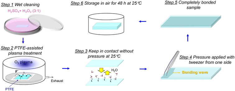 | ||
| Fig. 1 Schematic drawing of room-temperature bonding of glass chips via fluorinated plasma introduced by PTFE. | ||
2.2 Evaluation of bonding energy
To assess the bonding energy, the crack propagation length was recorded to calculate the bonding energy via the crack-opening method.29 This is the most convenient method to measure the strength of bonded samples. A razor with a thickness of tb (100 μm in this work) was inserted into the bonding interface. The bonding energy (γ) can be obtained via the following equation:where E is the Young's modulus for the fused silica substrate (6.6 × 10¹⁰ Pa), tw is the glass substrate thickness (7 × 10⁻⁴ m), and L is the crack propagation length.
2.3 Leakage test
Chips with two sets of microchannels bridged with 20 parallel nanochannels were fabricated on glass substrates for leakage tests, which is a standard micro/nano hybrid fluidic circuit for liquid manipulation in nanofluidic applications. In this micro/nanohybrid system, the microchannels facilitated the entry and regulation of liquids as well as the external connection on demand, while the nanochannels were employed for subsequent measurement. This nano-in-microfluidic system has distinctive advantages of steady liquid introduction, effective liquid exchange, and prevention of bubbles or dust entering the nanochannels. Therefore, the nano-in-microfluidic system is applicable not only for DNA/RNA analysis,21,30 but also for streaming potential/current measurement31 or in situ electrokinetic probing32 for the investigation of extended-nanospace chemistry, as an electrochemical reactor for enzymatic reactions33,34 to enhance reaction rates, the accurate active regulation of femtoliter-scale fluid flow,35etc. To be precise, the nanochannels were patterned on one side of the substrate by electron beam lithography, and two sets of microchannels were formed by photolithography on the other substrate, both of which were then subjected to plasma dry etching. Moreover, inlet/outlet holes at the end of microchannels were also drilled. The patterned glass substrates integrated by the abovementioned PTFE-assisted modification were ready to undergo leakage tests. Herein, we designed and developed a two-channel high-pressure liquid introduction system instead of a common air controller to inject sample solutions into the micro and nanochannels under a wide pressure range (50 kPa–2 MPa), which will be illustrated in detail later. By pressure switching and blocking one of the inlet holes of a microchannel, a fluorescent sample solution would be pressurized into nanochannels and another microchannel. Eventually, the channels filled with sample solution and leakage at the bonding interface could be checked on a nanometer-scale level using fluorescence microscopy. Considering the adsorption of fluorescent solution on the glass walls, sulforhodamine B (10 μmoL L−1) was chosen as the fluorescent dye and introduced into the microchannel to avoid interference results and ensure repeatability.3. Results and discussion
In order to elucidate the effect of PTFE-assisted modification, the chemical state of the glass substrates before and after activations was analyzed by X-ray photoelectron spectroscopy (XPS) first. As displayed in Fig. 2(a), the symmetric peak at 103.9 eV in the Si 2p spectrum of the pristine glass substrate was assigned to Si–O bonds.36 When the glass substrate was treated only with O2 plasma without a PTFE frame, the Si–O peak position shifted to a higher binding energy. This shift can be attributed to organic contaminant desorption on the pristine surface via chemical bond (e.g. C–Si–O) breakage. After O2 plasma activation, the contaminants decomposed into CO2 and H2O, and more Si–O dangling bonds were exposed owing to reactive oxygen radicals (ROS). Concurrently, Fig. 2(b) shows that there were no F-related signals detected on the O2 plasma-activated glass surface. However, a F signal emerged on the PTFE-assisted activated surface at 685.2 eV which was attributed to Si–F bonds.37 Due to the sputtering effect of ions with kinetic energy and the reactivity of ROS generated in O2 plasma, the C–F bonds of the PTFE were broken through chemical oxidation to form CO, CFxOy, and most importantly, fluorine radicals (F*), as shown in reaction (1).28,38 The gaseous CO and CFxOy could desorb from the PTFE surface, while neutral F* could diffuse onto the glass surface. These small amounts of reactive F* would not cause extensive bond breakage but partially broke Si–O bonds to terminate the glass surface with Si–F following exothermic reaction.39 Given that the essence of PTFE-assisted modification is the introduction of F*, this functionalization can also be denoted as (O2 + F*) plasma activation. | (1) |
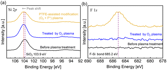 | ||
| Fig. 2 XPS (a) Si 2p and (b) F 1s core level spectra of glass substrates before and after activations. | ||
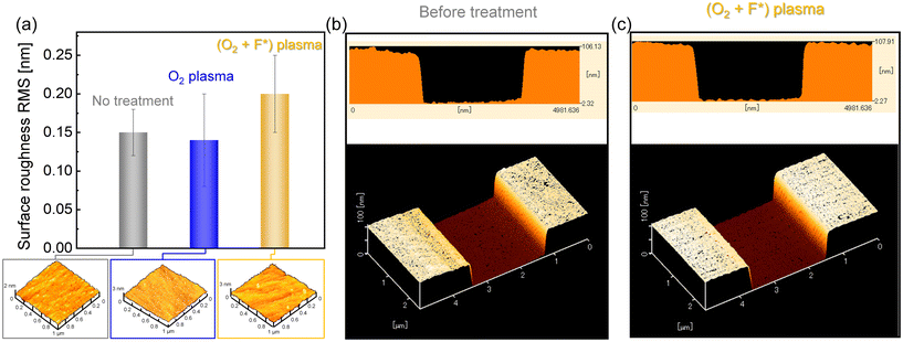
Albeit a fluorinated glass surface has been formed via (O2 + F*) plasma activation due to the assistance of PTFE, the surface morphology is an important factor that represents the real contact area between the surfaces to assess whether bonding can occur at room temperature. Evaluation of surface roughness in terms of root-mean-square (RMS) values and three-dimensional morphology analysis was achieved by atomic force microscopy (AFM). According to the reduced RMS values (<0.15 nm) shown in Fig. 3(a), it is indicated that the glass surface was slightly flattened after O2 plasma activation due to the desorption of contaminants. In contrast, the glass surface was roughened with the addition of F* in O2 plasma, and the average RMS value increased to 0.2 nm, even exceeding that of the bare glass surface. Since fluorine-containing gas plays an important role in the etching of SiO2 during semiconductor fabrication in industry, the slightly rougher glass surface obtained via (O2 + F*) plasma can be attributed to the etching effect of F*. Due to the low concentration of F* radicals, however, the surface morphology has not deteriorated further, and was still smooth enough (<0.5 nm) and conducive to room-temperature bonding. Moreover, AFM 3D images of glass substrates fabricated with nanochannels (100 nm in depth, 2 μm in width) before and after (O2 + F*) plasma activation are also displayed in Fig. 3(b) and (c). It can be observed that there is little change in the morphology of the nanochannels after (O2 + F*) plasma activation, indicating that the low concentration of F* will not damage the precise nanostructures on the glass substrate. Therefore, due to the cleaning effect of ROS and the etching action of F*, (O2 + F*) plasma currently appears to be a viable candidate for bonding glass substrates with complex nanostructures.
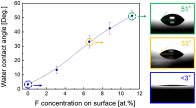
Though Si–F groups have been established on the smooth glass surface, the resultant surface energy ought to be further appraised for the correlation between the surface energy and bonding difficulty. According to the Young equation,40 wettability represents the surface energy which can be obtained by the water contact angle test. Fig. 4 presents the water contact angle of the glass surface as a function of F concentration on the surface. When the F concentration was reduced to 0 (O2 plasma activation), water droplets spread rapidly on the surface because of the construction of high-density –OH functional groups, and the final contact angle was stabilized at 3°. With the incorporation of sufficient –OH groups, the bonding wave was prone to propagating across the interface even with slight pressure applied with a tweezer. With the addition of F atoms, the contact angle increased significantly and could reach 51° when the F concentration was 11.2%. The relatively hydrophobic glass surface realized via (O2 + F*) plasma was attributed to the electronegativity of F, causing the polar hydrophobicity.41 However, the room temperature bonding could not be realized with this high concentration, indicating that excessive F atoms had a detrimental effect on bonding.
Considering the effect of fluorination, it is necessary to optimize the F concentration to achieve optimal bonding energy. Without the plasma treatment, the glass substrates were almost impossible to bond, and a fairly weak bonding energy of 0.125 J m−2 was obtained, as displayed in Fig. 5(a). Once the surfaces were activated by O2 plasma, the bonding strength was rapidly improved to 0.6 J m−2 after room temperature storage for 48 h, though it was still not robust enough for nanofluidic applications. Subsequently, the optimal F concentration was screened as 5% with the assistance of PTFE, obtaining a maximum bonding energy of 1.534 J m−2 with a crack opening length of 10.85 mm, as displayed in Fig. 5(b). In addition, a tensile test was also performed for the glass–glass interface with maximum bonding energy. As shown in Fig. 5(c), the room-temperature bonding interface exhibited good bonding strength with a maximum value of 11.3 MPa. However, the further introduction of F atoms could degrade the bonding energy, which was in accordance with the contact angle results. Furthermore, the activated surfaces with optimal F concentrations should be bonded without long-term exposure to preserve surface reactivity. Otherwise, the bonding strength and area would inevitably deteriorate. Fig. S4(a)† presents the bondability of activated surfaces with different air exposure times before bonding in an atmosphere with RH = 75%. Combined with Fig. S4(b),† it can be noted that optimal strength and bonding area could be attained simultaneously via timely bonding. However, one can notice that the bonding strength decreased slightly when the functionalized surfaces were bonded within 0.5 h, but still exceeded 8 MPa. With the prolongation of exposure time, the bonding strength was degraded further, and obvious unbonded regions with Newton rings were observed, as depicted in Fig. S4(c).† Ultimately, the surface became completely inactive after 2.5 hours of exposure. Therefore, a maximum storage time of 0.5 h in an atmosphere of RH = 75% was recommended to ensure bonding quality. Similarly, Xu et al.42 introduced F* on glass surfaces via a mixture of O2/CF4 plasma to obtain an optimal glass–glass bonding energy (1.12 J m−2) at room temperature. However, the flow rate of CF4 should be precisely controlled at 0.5 sccm via accurate gas flow controllers, which are expensive to equip with a commercial plasma chamber. Therefore, it is a more convenient and cost-effective solution to generate F* from PTFE. Moreover, it has been reported that the bonding energy of O2 plasma-activated Si–Si pairs can be saturated via long-term storage like 4000 h,43 indicating the sufficient occurrence of reaction between the hydroxylated interface. Similarly, it can be speculated that the glass–glass interface obtained by O2 plasma activation can be further strengthened via storage, whereas this duration could be effectively shortened via (O2 + F*) plasma treatment.
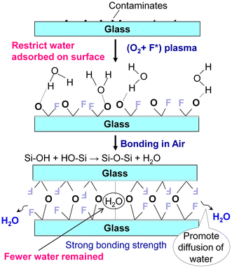
Combining the above results, the mechanism of room-temperature bonding via PTFE-assisted plasma modification can be illustrated, as shown in Fig. 6. When the glass surface was exposed to O2 plasma, a sufficiently smooth, hydrophilic surface terminated with sufficient –OH groups was achieved. A hydrogen network could be formed between the hydroxylated glass surfaces with the help of water molecules, determining whether bonding can take place.44 With increasing temperature or prolonged storage, the weak hydrogen bonds could be converted into strong covalent bonds according to the dehydration reaction (2), which is reversible up to 425 °C.45 The more by-product H2O molecules diffused from the interface, the more Si–O–Si covalent bonds were formed, which is more conducive to the strengthening of the interface. Therefore, the interfacial structure had an important influence on the enhancement of bonding energy.
| Si–OH + HO–Si → Si–O–Si + H2O | (2) |
| Si–OH + F–Si → Si–O–Si + HF | (3) |
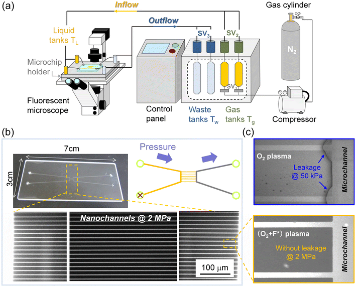
Regarding room-temperature bonded glass substrates, there is an urgent need to confirm whether the glass modified via PTFE met the requirements for nanofluidic devices. Thereby, a leakage test was applied to the glass substrates fabricated with micro and nanochannels. Since the nanofluidic channels usually should be able to withstand high pressures of hundreds of kilopascals, here the fluorescent solution was driven into the channels by a self-designed two-channel high-pressure liquid introduction system to verify the bonding strength, which can provide continuous, precise, and higher pressure (50 kPa–2 MPa) required for common nanofluidic applications. As illustrated in Fig. 7(a), N2 gas was generated from a gas cylinder and the gas pressure was increased up to a maximum of 4.4 MPa using a compressor. The pressurized N2 gas was divided into two channels and stored in two gas tanks (Tg), and the gas pressure in the Tg could be controlled by the connecting solenoid valves SV1. Afterward, by opening the solenoid valves SV2, the sample solution (sulforhodamine B) was pushed from the gas tanks into the connecting liquid tanks (TL), ready to be introduced into the nanofluidic chip fixed on a stainless steel microchip holder. The connections between the TL and nanofluidic chip were sealed with Teflon O-rings. It is noteworthy that one of the liquid tanks was filled with sample solutions from the gas tank, while another liquid tank was just filled with pressurized gas to ensure the diffusion of the solution from one side microchannel to the other via 20 bridging nanochannels. As sulforhodamine B was driven into the nanofluidic chip, leakage could be observed via fluorescence microscopy when the bonding area was filled with fluorescent solution. Eventually, the fluorescent solution could be collected and recycled in waste tanks (Tw) via solenoid valves SV3 to keep the experiment environmentally friendly. The actions of all valves could be controlled through an LCD touch panel.
Based on the abovementioned pressure-driven fluidic control system, Fig. 7(b) shows that sulforhodamine B was introduced into the left side microchannel and center nanochannels (400 nm in width, 200 nm in depth, 700 μm in length), which were sealed by (O2 + F*) plasma activation at room temperature, and effused from the right side microchannel. Due to the higher Laplace pressure in nanochannels, leakage is more likely to be observed at the nanochannels and connections of the micro and nanochannels. Fig. 7(b) presents that strong fluorescence was observed in all the 700 μm long nanochannels with the continuous introduction of sulforhodamine B at a pressure of 2 MPa, whereas no fluorescence was observed at the bonding interface between the nanochannels, revealing the defect-free interface and sufficient bonding strength. Moreover, as displayed in Fig. 7(c), the enlarged fluorescence image illustrated that a hermetic seal was realized at the connection of the right microchannel and nanochannels, which suggested the successful introduction of the solution into the microchannel via bridging nanochannels without leakage. The leak-free glass–glass interface verified the capability of nanofluidic devices assembled via (O2 + F*) plasma to withstand high pressure. In contrast, a fluorescence signal was detected at the connection of the microchannel and nanochannels formed via O2 plasma activation even at a pressure of 50 kPa, indicating the risk of substrate separation under common nanofluidic conditions. Therefore, the stable and robust glass–glass interface fabricated via PTFE-assisted plasma modification demonstrated broad prospects for applications spanning sensing, medical diagnostics, high-pressure nanochromatography, etc.
In addition, the direct transmittance of bulk substrates and bonded glass pairs was analyzed using a UV-vis spectrophotometer in the wavelength range of 200–800 nm. As presented in Fig. 8, the transmittance of the bulk glass substrate exceeded 93% in the range of 400 nm to 800 nm, indicating the extraordinary optical properties of the glass substrate as a nanofluidic platform. However, the optical transmittance was reduced by less than 1% for the glass pairs bonded at room temperature via (O2 + F*) plasma, exhibiting relatively high transparency which was close to that of the bulk glass substrate. Given the light absorption by the glass itself, it can be concluded that not only was there no defect at the bonding interface, but also the fluorinated SiOxFy layer had little effect on the decrease in optical transmittance. Thus, the defect-free bonded glass pairs activated by (O2 + F*) plasma demonstrated potential for future high-speed, high-sensitivity, and high-resolution optical detection or liquid sensing.
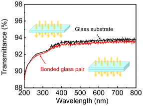 | ||
| Fig. 8 UV-vis transmission spectra of the bulk glass (700 μm thick) and the glass/glass bonded pair (1400 μm thick in total). | ||
4. Conclusion
In summary, we developed a strong and nano-structure friendly PTFE-assisted plasma modification strategy for glass–glass bonding at room temperature. Because of the cleaning effect, sputtering effect, and chemical reactivity of O2 plasma, fluorine radicals (F*) were generated from PTFE in a commercialized reactive ion etching plasma chamber, and the glass surface was flattened and functionalized effectively within 40 s. Although the etching effect of fluorine-containing gas on SiO2 was extensively proved, the addition of trace F* could obtain a smooth glass surface and maintain the profile of precise nanochannels. Without a requirement for immersion in dangerous chemicals such as HF, a Si–OH and Si–F terminated glass surface with fluorinated silica oxide in the subsurface was obtained via the (O2 + F*) plasma treatment, and this fluorinated SiOxFy layer had little effect on the light transmittance. By controlling the F concentration on the surface, a maximum bonding energy of 1.534 J m−2 was achieved after room-temperature storage for 48 h, which was almost three times stronger than that of the interface realized by only O2 plasma activation. Moreover, the capability of this PTFE-assisted plasma modification strategy for nanofluidic devices was verified, and a leak-free glass–glass interface with high-pressure resistance (2 MPa) would exhibit great potential for applications immobilized by temperature-sensitive functional components.Conflicts of interest
There are no conflicts to declare.Acknowledgements
This work was financially supported by the National Natural Science Foundation of China (Grant No. 51975151 and 92164105), the Heilongjiang Provincial Natural Science Foundation of China under grant LH2019E041, and the Heilongjiang Touyan Innovation Team Program (HITTY-20190013). The authors also acknowledge financial support from the Core Research for Evolutional Science and Technology (CREST) program of the Japan Science and Technology (JST) via grant no. JPMJCR14G1.References
- D. R. Reyes, D. Iossifidis, P. Auroux and A. Manz, Anal. Chem., 2002, 74, 2623–2636 CrossRef CAS PubMed.
- D. Najjar, J. Rainbow, S. Sharma Timilsina, P. Jolly, H. de Puig, M. Yafia, N. Durr, H. Sallum, G. Alter, J. Z. Li, X. G. Yu, D. R. Walt, J. A. Paradiso, P. Estrela, J. J. Collins and D. E. Ingber, Nat. Biomed. Eng., 2022, 6, 968–978 CrossRef CAS PubMed.
- M. Yafia, O. Ymbern, A. O. Olanrewaju, A. Parandakh, A. Sohrabi Kashani, J. Renault, Z. Jin, G. Kim, A. Ng and D. Juncker, Nature, 2022, 605, 464–469 CrossRef CAS PubMed.
- H. Hisamoto, Y. Shimizu, K. Uchiyama, M. Tokeshi, Y. Kikutani, A. Hibara and T. Kitamori, Anal. Chem., 2003, 75, 350–354 CrossRef CAS PubMed.
- H. Hisamoto, T. Saito, M. Tokeshi, A. Hibara and T. Kitamori, Chem. Commun., 2001, 2662–2663 RSC.
- S. I. Funano, N. Ota and Y. Tanaka, Lab Chip, 2021, 21, 2244–2254 RSC.
- Y. Xu, C. Wang, Y. Dong, L. Li, K. Jang, K. Mawatari, T. Suga and T. Kitamori, Anal. Bioanal. Chem., 2012, 402, 1011–1018 CrossRef CAS PubMed.
- D. I. Rozkiewicz, B. J. Ravoo and D. N. Reinhoudt, Supramol. Chem. Org.–Inorg. Hybrid Mater., 2010, 433–466 CAS.
- Y. Ding, S. Garland, M. Howland, A. Revzin and T. Pan, Adv. Mater., 2011, 23, 5551–5556 CrossRef CAS PubMed.
- B. Samel, M. K. Chowdhury and G. Stemme, J. Micromech. Microeng., 2007, 17, 1710–1714 CrossRef CAS.
- L. Yu, F. E. H. Tay, G. Xu, B. Chen, M. Avram and C. Iliescu, J. Phys.: Conf. Ser., 2006, 34, 776–781 CrossRef CAS.
- X. Zhou, S. Virasawmy and C. Quan, Microsyst. Technol., 2009, 15, 573–580 CrossRef CAS.
- J. Q. Lu, J. J. McMahon and R. J. Gutmann, Mater. Res. Soc. Symp. Proc., 2009, 1112, 69–80 Search PubMed.
- N. Y. Lee and B. H. Chung, Langmuir, 2009, 25, 3861–3866 CrossRef CAS PubMed.
- V. Sunkara and Y. K. Cho, ACS Appl. Mater. Interfaces, 2012, 4, 6537–6544 CrossRef CAS PubMed.
- J. Xu, C. Wang, S. Zhou, R. Zhang and Y. Tian, Ceram. Int., 2019, 45, 16670–16675 CrossRef CAS.
- M. Zhang, J. Zhao and L. Gao, Sens. Actuators, A, 2008, 141, 213–216 CrossRef CAS.
- L. Tang and N. Y. Lee, Lab Chip, 2010, 10, 1274–1280 RSC.
- J. Bart, R. Tiggelaar, M. Yang, S. Schlautmann, H. Zuilhof and H. Gardeniers, Lab Chip, 2009, 9, 3481–3488 RSC.
- M. Iwakura, D. Nakamura, T. Takenawa and Y. Mitsuishi, Protein Eng., 2001, 14, 583–589 CrossRef CAS PubMed.
- B. Renberg, K. Sato, K. Mawatari, N. Idota, T. Tsukahara and T. Kitamori, Lab Chip, 2009, 9, 1517–1523 RSC.
- M. M. R. Howlader, S. Suehara and T. Suga, Sens. Actuators, A, 2006, 127, 31–36 CrossRef CAS.
- K. Takeuchi, F. Mu, Y. Matsumoto and T. Suga, Adv. Mater. Interfaces, 2021, 8, 1–8 Search PubMed.
- Z. J. Jia, Q. Fang and Z. L. Fang, Anal. Chem., 2004, 76, 5597–5602 CrossRef CAS PubMed.
- H. Nakanishi, T. Nishimoto, M. Kanai, T. Saitoh, R. Nakamura, T. Yoshida and S. Shoji, Sens. Actuators, A, 2000, 83, 136–141 CrossRef CAS.
- L. Chen, G. Luo, K. Liu, J. Ma, B. Yao, Y. Yan and Y. Wang, Sens. Actuators, B, 2006, 119, 335–344 CrossRef CAS.
- Y. Wang, Y. Xu, S. Dong, P. Wang, W. Chen, Z. Lu, D. Ye, B. Pan, D. Wu, C. D. Vecitis and G. Gao, Nat. Commun., 2021, 12, 1–8 CrossRef PubMed.
- G. Primc, Polymer, 2020, 12, 1–7 Search PubMed.
- W. P. Maszara, G. Goetz, A. Caviglia and J. B. McKitterick, J. Appl. Phys., 1988, 64, 4943–4950 CrossRef CAS.
- F. Persson, J. Fritzsche, K. U. Mir, M. Modesti, F. Westerlund and J. O. Tegenfeldt, Nano Lett., 2012, 12, 2260–2265 CrossRef CAS PubMed.
- K. Morikawa, K. Mawatari, M. Kato, T. Tsukahara and T. Kitamori, Lab Chip, 2010, 10, 871–875 RSC.
- Y. Xu and B. Xu, Small, 2015, 11, 6165–6171 CrossRef CAS PubMed.
- T. Tsukahara, K. Mawatari, A. Hibara and T. Kitamori, Anal. Bioanal. Chem., 2008, 391, 2745–2752 CrossRef CAS PubMed.
- W. Xu, E. Foster, C. Ma and P. W. Bohn, Microfluid. Nanofluid., 2015, 19, 1181–1189 CrossRef CAS PubMed.
- Y. Xu, M. Shinomiya and A. Harada, Adv. Mater., 2016, 28, 2209–2216 CrossRef CAS PubMed.
- A. Kaur, P. Chahal and T. Hogan, IEEE Electron Device Lett., 2016, 37, 142–145 CAS.
- C. Wang and T. Suga, ECS J. Solid State Sci. Technol., 2016, 5, P393–P395 CrossRef CAS.
- J. A. Colony and E. L. Sanford, Nasa Tm/100681, 1987, p. 10.
- D. J. Oostra, J. Vac. Sci. Technol., B: Microelectron. Process. Phenom., 1986, 4, 1278 CrossRef CAS.
- M. A. Miranda, A. Ghosh, G. Mahmodi, S. Xie, M. Shaw, S. Kim, M. J. Krzmarzick, D. J. Lampert and C. P. Aichele, Water, 2022, 14, 880 CrossRef CAS.
- S. Roy, B. Biswas, N. Ghosh, P. C. Singh and J. A. Mondal, J. Phys. Chem. C, 2019, 123, 27012–27019 CrossRef CAS.
- Y. Xu, C. Wang, L. Li, N. Matsumoto, K. Jang, Y. Dong, K. Mawatari, T. Suga and T. Kitamori, Lab Chip, 2013, 13, 1048–1052 RSC.
- T. Plach, K. Hingerl, S. Tollabimazraehno, G. Hesser, V. Dragoi and M. Wimplinger, J. Appl. Phys., 2013, 113, 094905 CrossRef.
- Q. Y. Tong and U. M. Gösele, Adv. Mater., 1999, 11, 1409–1425 CrossRef CAS.
- Q. Y. Tong and U. M. Gösele, Semiconductor Wafer Bonding: Science and Technology, Wiley, New York, 1999 Search PubMed.
- A. Kazor, C. Jeynes and I. W. Boyd, Appl. Phys. Lett., 1994, 65, 1572–1574 CrossRef CAS.
- V. Pankov, J. C. Alonso and A. Ortiz, J. Appl. Phys., 1999, 86, 275–280 CrossRef CAS.
- H. Takagi, Y. Kurashima, A. Takamizawa, T. Ikegami and S. Yanagimachi, Jpn. J. Appl. Phys., 2017, 57, 02BA04 CrossRef.
Footnote |
| † Electronic supplementary information (ESI) available: The characterization of bonding efficiency with different relative humidities, and room temperature bonding energy of glass–glass as a function of storage time in ambient air. The XPS compositional depth analysis of the glass surface activated via (O2 + F*) plasma. Schematic of five positions on the fused-silica glass surface for the XPS measurements and the atomic concentrations (at%) of fluorine at the corresponding positions after (O2 + F*) plasma treatment for 40 s. The evaluation of bondability of (O2 + F*) plasma activated surfaces with different air exposure times before bonding at RH = 75% in the atmosphere. See DOI: https://doi.org/10.1039/d3lc00169e |
| This journal is © The Royal Society of Chemistry 2023 |


