 Open Access Article
Resistive switching in benzylammonium-based Ruddlesden–Popper layered hybrid perovskites for non-volatile memory and neuromorphic computing†
Mubashir M.
Ganaie
 a,
Gianluca
Bravetti
 b,
Satyajit
Sahu
 a,
Mahesh
Kumar
 *c and
Jovana V.
Milić
 *b
*b
aDepartment of Physics, Indian Institute of Technology, Jodhpur 342037, India
bSmart Energy Materials, Adolphe Merkle Institute, University of Fribourg, Fribourg 1700, Switzerland. E-mail: jovana.milic@unifr.ch
cDepartment of Electrical Engineering, Indian Institute of Technology Jodhpur, Jodhpur 342037, India. E-mail: mkumar@iitj-ac-in
First published on 3rd January 2024
Abstract
Artificial synapses based on resistive switching have emerged as a promising avenue for brain-inspired computing. Hybrid metal halide perovskites have provided the opportunity to simplify resistive switching device architectures due to their mixed electronic–ionic conduction, yet the instabilities under operating conditions compromise their reliability. We demonstrate reliable resistive switching and synaptic behaviour in layered benzylammonium (BzA) based halide perovskites of (BzA)2PbX4 composition (X = Br, I), showing a transformation of the resistive switching from digital to analog with the change of the halide anion. While (BzA)2PbI4 devices demonstrate gradual set and reset processes with reduced power consumption, the (BzA)2PbBr4 system features a more abrupt switching behaviour. Moreover, the iodide-based system displays excellent retention and endurance, whereas bromide-based devices achieve a superior on/off ratio. The underlying mechanism is attributed to the migration of halide ions and the formation of halide vacancy conductive filaments. As a result, the corresponding devices emulate synaptic characteristics, demonstrating the potential for neuromorphic computing. Such resistive switching and synaptic behaviour highlight (BzA)2PbX4 perovskites as promising candidates for non-volatile memory and neuromorphic computing.
Introduction
Resistive switching has garnered significant attention in non-volatile memory technology due to its rapid switching speed, remarkable endurance, exceptional density, and minimal power consumption.1 The principle of resistive switching is associated with resistive random-access memory (RRAM) operation, characterized by an abrupt variation in resistance.2 These systems can be classified into digital or analog, depending on whether the resistive switching effect is abrupt or gradual. While digital memristors are primarily studied for non-volatile memory applications, analog ones hold significant potential in the field of neuromorphic computing.2 To this end, two-terminal devices with a vertical metal–insulator–metal structure have provided a simplified design for artificial synapses owing to their capability to mimic the transmission properties of biological synapses.3 Such devices play a pivotal role as fundamental functional units in neuromorphic computing,4 where electrical stimuli must transfer from a pre-synaptic to a post-synaptic neuron for an artificial synapse to operate. In a ‘memristor’, a resistive switching memory element that can mimic the operation of a biological system, one metal electrode serves as a pre-neuron, another as a post-neuron, and the insulating layer acts as the synapse.5,6 A wide range of materials have demonstrated the ability to exhibit resistive switching, including polymers,7 organic materials,8 transition metal dichalcogenides,9 binary oxides,10 and perovskites.11 While oxides are the most extensively studied materials for resistive memories, their efficacy is impeded by the difficult fabrication, high-power consumption, and lack of precise control over filament formation that is associated with memristive functions, which compromises their performance.12,13 In particular, the necessity of high-temperature processing and vacuum conditions limits the application of perovskite oxide materials in RRAM.14 Alternatively, hybrid halide perovskite materials have emerged as promising contenders in the realm of optoelectronic devices, notably in applications such as photovoltaics,15 light-emitting diodes,16 lasing,17 and photodetectors.18,19 Due to their mixed ionic–electronic conduction,20,21 low leakage currents, and tuneable band gap, hybrid metal halide perovskites have extended their utility to memory devices,13,22,23 offering the possibility of integrating the benefits of both inorganic and organic resistive switching. However, the instability of halide perovskites under operating conditions poses a challenge for their application.21,24Toward overcoming the instability of metal halide perovskites, layered (2D) hybrid perovskites incorporating larger organic moieties have shown potential for stabilizing perovskite materials and their devices toward more reliable memory elements.25,26 These materials are often defined by the general formulation of S2An+1MX4, where S and A are (i.e., alkyl or arylammonium) spacers and central (e.g., methylammonium (MA), formamidinium (FA), etc.) organic cations, respectively, M is a divalent metal ion (mostly Pb2+) and X halide anion (I−, Br−, or Cl−).22,25,26 The value of n represents the number of {MX6} corner-sharing octahedra between organic spacer (S) layers. While these systems present a diverse class of materials defined by different compositional elements and number of layers (n), they are mostly associated with Ruddlesden–Popper (RP) phases formed by van der Waals interactions between spacer cations with a half-a-unit-cell displacement between the adjacent slabs (Fig. 1).26,27 As a result, the 2D perovskite structure exhibits anisotropic charge transport, particularly in the out-of-plane direction, and this unique characteristic holds promise for designing resistive memories with low programming currents.28 However, the application of 2D perovskites in resistive switching memories has so far been limited, primarily relying on archetypical n-butylammonium (BA) and 2-phenylethylammonium (PEA) based materials.22,28 For instance, it was shown that the reduction of dimensionality from 3D to 2D induced the resistive switching properties of BA/MA-based RP phases with an improvement in the endurance and on/off ratios. The 2D structure was also found to be advantageous for the formation of a conductive filament, primarily due to the anisotropic migration of defects.28 Similarly, 2D RP (PEA)2PbBr4 perovskite single crystals exhibited resistive switching behaviour with significantly reduced currents of 10 pA, attributed to the mixed transport.22 A recent study also reported an exceptionally high on/off ratio of 109 using a quasi-2D perovskite based on (PEA)2Cs3Pb4I13 composition, higher than that of the 3D CsPbI3, which was attributed to the wider bandgap and thus an increased Schottky barrier.29 The composition of halide perovskite has also been found to impact its switching properties in 3D CH3NH3PbX3 (X = I, Br), where the set voltage was found to decrease when the iodide is replaced by bromide due to the lower barrier for Br− migration compared to I− ions.30 This is unexploited in 2D perovskites, which still remain underrepresented in resistive switching devices despite their potential.
Here, we report the resistive switching behaviour of layered benzylammonium (BzA) based hybrid halide perovskite of (BzA)2PbX4 (X = Br, I) composition. The memory devices based on a simple Al/(BzA)2PbX4/fluorine-doped tin oxide (FTO) architecture exhibited bipolar resistive switching behaviour with low switching voltage, good data retention, and excellent endurance. Moreover, we observed an unusual transformation from digital to analog resistive switching upon the substitution of Br with I ions. A model is proposed in which a conductive filament is formed by halide vacancies to explain the underlying mechanism.31 Finally, voltage pulses were applied to the (BzA)2PbI4 device to validate its capability to emulate a synapse and function as an artificial synapse.32 The observed gradual set and reset behaviour of the device signifies its potential for neuromorphic applications, where the ability to tune conductance dynamically is highly desirable. The artificial synapse effectively emulated key synaptic characteristics, such as potentiation, depression, and paired-pulse facilitation.5 This study thereby reveals unique resistive switching characteristics for layered BzA-based hybrid halide perovskites, providing a better understanding of their memristive effects and revealing the potential for neuromorphic computing in the future.
Results and discussion
The resistive switching properties of (BzA)2PbX4 (X = I, Br) perovskites were studied in a metal–insulator–metal device based on a thin film spin-coated on the FTO substrate and top circular Al electrode contacts (Fig. 1). The experimental details are provided in the Experimental Section of the Electronic Supporting Information (ESI,† Fig. S1–S5). Layered (2D) perovskite materials were prepared mechanosynthetically by ball-milling, followed by solution-based spin-coating and subsequent annealing. The formation of a 2D perovskite was evidenced by X-ray diffraction, UV-vis absorption, and photoluminescence spectroscopy (Fig. S1, ESI†).27Resistive switching characteristics of the Al/(BzA)2PbX4/FTO devices reveal a distinct bipolar switching (Fig. 2a and b). Digital switching is observed in (BzA)2PbBr4 upon application of voltage in the range between +2 V and −4 V (Fig. 2a).33 Upon sweeping the voltage from 0 to 2 V, an abrupt transition from a high (HRS) to a low resistance state (LRS) is observed at +1.04 V, indicating the set process. The LRS persisted until a negative bias voltage was applied, after which the state reverted back to HRS at −1.33 V, signifying the reset process. In contrast, Al/(BzA)2PbI4/FTO showed a more gradual set and reset (Fig. 2b). The set and reset voltages of +0.5 V and −1 V for (BzA)2PbI4 were also smaller, and the device featured lower power consumption, with the estimated set and reset powers of 0.63 mW (at 0.5 V and 1.26 mA) and 12.25 mW (at −1 V and 12.2 mA), respectively. In addition, current–voltage characteristics exhibited a negative differential resistance (NDR), where the current decreased as the voltage increased after reset, which is relevant for achieving diverse resistance states in neuromorphic computing applications.34
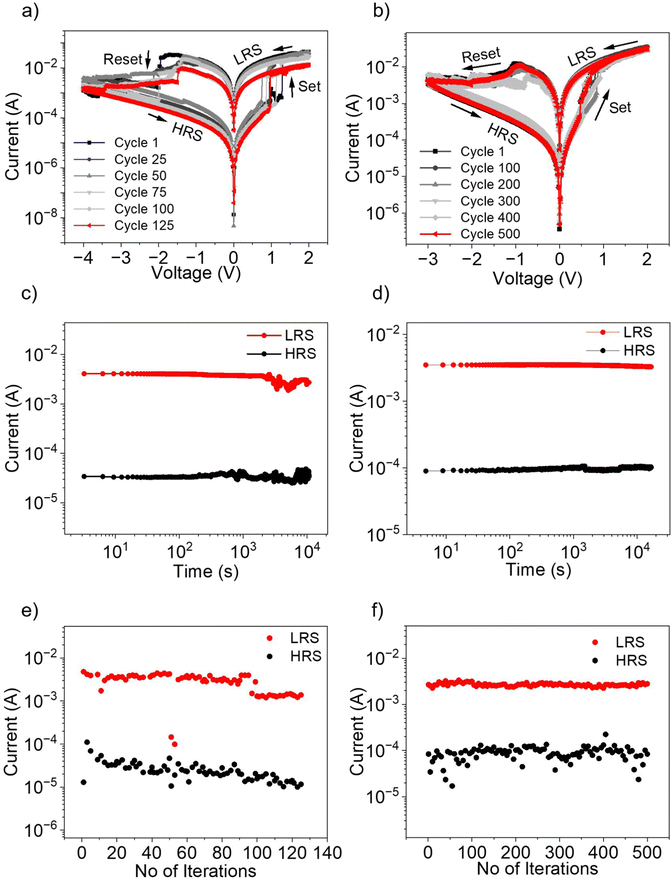 | ||
| Fig. 2 Resistive switching in bromide (left) and iodide (right) based layered hybrid perovskites. Current–voltage characteristics for bipolar resistive (a) digital switching in (BzA)2PbBr4 and (b) analog switching in (BzA)2PbI4 devices at the voltage scan rate of 20 mV and 8 ms time sweep. More information about the frequency and contact dependence is detailed in ESI† (Fig. S3 and S4). To calculate the set voltage for the I-based system, the current–voltage curve was replotted on a linear scale to visualise the point where the current starts increasing (Fig. S5, ESI†). (c) and (d) Retention time and (e) and (f) endurance over repeated cycles for resistive switching devices at 0.2 V bias over (e) 125 cycles in (BzA)2PbBr4-based system and (f) 500 cycles in (BzA)2PbI4 -based system. Current in HRS (black) and LRS (red) was read at +0.2 V for the endurance and retention tests. | ||
To assess the nonvolatility and reliability of each state (i.e., resistance level) in Al/(BzA)2PbX4/FTO devices, retention time and endurance characteristics were monitored (Fig. 2c–f). The iodide-based (X = I) system exhibited better retention and endurance than the bromide-based (X = Br) system by showing a stable switching for more than 500 cycles with a retention time of 1.5 × 10⁴ s (Fig. 2d and f), whereas the bromide-based system showed a superior on/off ratio of >102 as compared to iodide system (Fig. 2c and e). These characteristics highlight the non-volatile potential of the devices that can be further optimised in terms of morphology, thickness, and device architecture beyond the scope of this study, such as by tailoring contact layers and using interlayers to reach longer retention time and better on/off ratios for practical applications.
To ensure that the device can reliably store and retrieve data, write-read-erase-read (WRER) pulses were applied (Fig. 3a and Fig. S6, ESI†). A pulse voltage of 2 V was first applied for a duration of 4 s to write data into the (BzA)2PbBr4 device (Fig. 3a). This voltage pulse causes the resistive state of the device to change and store the data. After the writing process, a read voltage of 0.2 V was applied for 6 s to verify the data stored. Finally, an erase voltage of −4 V was applied for 4 s, causing the resistive state to change and erase the data. Once the erase process was complete, a pulse voltage of 0.2 V was used for 6 s to read the erased state (Fig. 3b). A reliable switching between these states was observed for 100 WRER cycles. Moreover, a comparable procedure was applied to the (BzA)2PbI4 system, with an erase pulse of −3 V instead of −4 V (Fig. S6, ESI†), evidencing the utility of the system for storing and retrieving data.
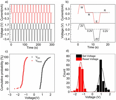 | ||
| Fig. 3 Bromide-based perovskite memory data storage and retrieval. (a) Write-read-erase-read (WRER) cycles. (b) Enlarged view of 1st WRER cycle indicating write (W), read (R), and erase (E) states with the corresponding voltage bias. (c) Cumulative probability for set and reset voltages based on 125 cycles. (d) Statistical distribution of set and reset voltages with Gaussian fitted curve. WRER cycles for the iodide-based system are detailed in Fig. S6 of the ESI.† | ||
The practicality of WRER cycles for RRAM applications was further assessed for their consistency and reliability by analysing the uniformity in switching voltages. For this purpose, cumulative probabilities of the set and reset voltages of the (BzA)2PbBr4 device were calculated using data obtained from 125 switching cycles (Fig. 3c and d). The statistical distribution of set and reset voltages indicated the voltage range where the switching occurs (Fig. 3c). The set voltage range was found to be between 0.69 V to 1.98 V with an average of 1.04 V, while the reset voltage was distributed between −0.81 V and −2.38 V with an average of −1.33 V in (BzA)2PbBr4 (Fig. 3d). This voltage profile permits reliable and consistent switching in RRAM applications. The gradual switching behaviour in (BzA)2PbI4 devices, however, suggests a distinct operation mechanism that is more relevant in the design of artificial synapses (Fig. 4).
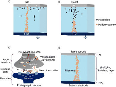
The differences in the resistance switching mechanism of (BzA)2PbX4 devices can be governed by the halide ion (X−) migration dynamics and the subsequent halide vacancy (VX) conductive filament formation under the influence of the applied electric field (Fig. 4a and b).22,23 Specifically, when a positive voltage is applied, negatively charged halide ions migrate toward the top electrode. Such a migration of ions leads to the formation of halide vacancies, which are gradually accumulating and contributing to the formation of a halide vacancy conductive filament in the LRS (Fig. 4a). When a negative voltage is applied to the top electrode, halide ions migrate in the opposite direction, causing the ‘rupture’ of the filament, switching the device to the HRS (Fig. 4b). This halide ion dynamics can be related to the distinct digital and analog switching mechanisms, as analog switching can be associated with the gradual migration of iodide ions, whereas digital switching corresponds to the faster migration of bromide ions.30 With lower activation energy, bromide ions exhibit faster migration, whereas higher activation energy of iodide vacancies hinders rapid migration,30 leading to digital switching in (BzA)2PbBr4 and a more gradual movement of iodide ions and, consequently, analog switching behaviour in (BzA)2PbI4.
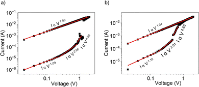
To gain a better understanding of the conduction mechanism, current–voltage characteristics were assessed for both bromide- and iodide-based devices (Fig. 5). In their HRS, the analysis of the double logarithmic scale discerns the presence of three distinctive conductive regimes (I–III). First, at low voltages, the curve exhibits a linear region with a slope close to unity, suggesting Ohmic conduction, which is dominated by thermally generated free charge carriers (I). Next, as the voltage increases, the deviations from linearity become apparent, marking the onset of space charge-limited conduction (SCLC). As the applied bias voltage is raised from 0.15 V to 0.46 V, the injected electrons dominate the conduction mechanism, resulting in a trap-unfilled SCLC where the current is closely proportional to the square of the bias voltage (II). In this case, the conduction may be expressed by the eqn (1):35
 | (1) |
The synaptic behaviour is often described by potentiation (i.e., increase in synaptic weight through a gradual current increase upon biasing) and depression (i.e., decrease in synaptic weight through gradual current decrease upon biasing), which represent the changes in the strength of the artificial synapse that mimics biological systems.5 Analog resistive switching behaviour observed in the current–voltage sweeps of (BzA)2PbI4 system suggested that it could exhibit potentiation and depression, which was assessed through pulse biases of +0.5 V and −1 V, respectively. Upon application of 20 positive pulses of +0.5 V, the current level increased gradually from around 0.74 to 1.1 mA, resembling synaptic potentiation (Fig. 6a and c). Subsequently, the application of 20 negative pulses of −1 V caused a gradual decrease in the current level from about 10.2 to 4.9 mA, mimicking synaptic depression (Fig. 6b and d). Accordingly, positive and negative pulses induce a weight change that leads to potentiation and depression. With positive pulses, iodide ions are expected to move towards the top electrode (Fig. 4), initiating the formation of filaments due to iodide vacancies, which would gradually enhance the conductance associated with potentiation. Similarly, negative pulses would induce the retrograde movement of ions towards the iodide vacancies, restoring the conductance to the original (lower) current state in a depression.22
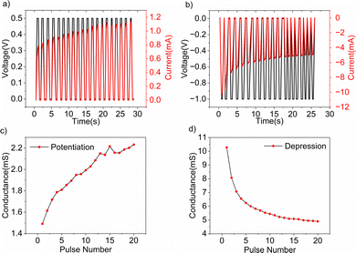 | ||
| Fig. 6 Synaptic behaviour in the iodide-based layered hybrid perovskite. (a) Gradual increase in current on applying consecutive 20 positive pulses of 379 ms width and 0.5 V height. Additional scans confirming the reliability are shown in the ESI† (Fig. S7). (b) A gradual decrease in current on the application of 20 negative pulses of 379 ms width and −1 V height. (c) Potentiation and (d) depression, mimicking the increase and decrease in synaptic weight, respectively. Additional information about the PPF effect is provided in Fig. S8 of the ESI.† | ||
The synaptic behaviour is relevant to neural signalling, which is commonly described by the paired-pulse facilitation (PPF), a synaptic plasticity phenomenon where the response of a neuron to a pair of stimuli is enhanced when the second stimulus is delivered shortly after the first one.37 This is an important mechanism for information processing and memory in the brain. Additional scans provide evidence of the PPF effect in (BzA)2PbI4 devices (Fig. S7 and S8, ESI†). The enhancement in the synaptic response can be related to the migration of iodide ions after the first stimulus, facilitating conduction in response to the second stimulus. Such emulation of key synaptic characteristics in the iodide-containing perovskite artificial synapse provides a proof-of-concept for its viability in neuromorphic systems that can be further explored in the future.
Conclusions
We investigated the resistive switching of benzylammonium (BzA) based (BzA)2PbX4 layered RP lead halide perovskites, showcasing their potential for non-volatile memory and neuromorphic computing applications. The study revealed a shift from digital to analog resistive switching through halide substitution, offering versatile functionality and reduced power consumption. The underlying mechanism was primarily attributed to halide ion migration and halide vacancy conductive filament formation. Both the bromide- and iodide-based systems exhibited high performances, with the former excelling in achieving a superior on/off ratio and the latter displaying excellent retention and endurance. The (BzA)2PbBr4 established reliable random-access data storage and retrieval capabilities through write-read-erase-read (WRER) pulses, complemented by consistent switching voltages for uniform performance in practical random-access memory applications. In addition, (BzA)2PbI4 demonstrated gradual (analog) set and reset processes, enhancing energy efficiency and emulating critical synaptic characteristics, such as potentiation, depression, and paired-pulse facilitation, showcasing its potential for neuromorphic computing. These resistive switching properties and synaptic behaviour position (BzA)2PbX4 layered hybrid halide perovskites as compelling candidates for advanced non-volatile memory and neuromorphic computing. This further contributes to the development and understanding of hybrid halide perovskites in the realm of emerging memory technologies.Experimental
Experimental details, including materials and methods, are provided in the Electronic Supplementary Information (ESI†). Data presented here can be accessed at the DOI: 10.5281/zenodo.10392068, and it is available under the license CC-BY-4.0 (Creative Commons Attribution-ShareAlike 4.0 International).Author contributions
M.M.G. led the project and conducted the experiments with the support of S.S. and G.B., who (mechano)synthesized the layered hybrid perovskites and performed their structural and optoelectronic characterization in powders and thin films. The project was conceptualized by J.V.M. and M.K., who supervised and directed it. All authors contributed to the manuscript.Conflicts of interest
There are no conflicts to declare.Acknowledgements
G. B. and J. V. M. acknowledge the Swiss National Science Foundation project no. 193174. The authors are grateful to Prof. Ullrich Steiner (Adolphe Merkle Institute, Fribourg, Switzerland) and DFG-SPP 186453 project for support.Notes and references
- R. Waser and M. Aono, Nat. Mater., 2007, 6, 833 CrossRef CAS PubMed.
- X. Zhao, Z. Wang, W. Li, S. Sun, H. Xu, P. Zhou, J. Xu, Y. Lin and Y. Liu, Adv. Funct. Mater., 2020, 30, 1910151 CrossRef CAS.
- R. Waser, R. Dittmann, C. Staikov and K. Szot, Adv. Mater., 2009, 21, 2632 CrossRef CAS PubMed.
- D. Ielmini and H.-S. P. Wong, Nat. Electron., 2018, 1, 333 CrossRef.
- S. G. Kim, J. S. Han, H. Kim, S. Y. Kim and H. W. Jang, Adv. Mater. Technol., 2018, 3, 1800457 CrossRef.
- A. Bou and J. Bisquert, J. Phys. Chem. B, 2021, 125, 9934 CrossRef CAS PubMed.
- Y. van de Burgt, E. Lubberman, E. J. Fuller, S. T. Keene, G. C. Faria, S. Agarwal, M. J. Marinella, A. Alec Talin and A. Salleo, Nat. Mater., 2017, 16, 414 CrossRef CAS PubMed.
- A. Betal, J. Bera and S. Sahu, J. Mater. Chem. C, 2023, 11, 4674 RSC.
- M. E. Pam, S. Li, T. Su, Y. C. Chien, Y. Li, Y. S. Ang and K. W. Ang, Adv. Mater., 2022, 34, 2202722 CrossRef CAS PubMed.
- I. H. Inoue, S. Yasuda, H. Akinaga and H. Takagi, Phys. Rev. B: Condens. Matter., 2008, 77, 35105 CrossRef.
- A. K. Shringi, A. Betal, S. Sahu and M. Kumar, Appl. Phys. Lett., 2021, 118, 263505 CrossRef CAS.
- S. Satapathi, K. Raj, Yukta and M. A. Afroz, Phys. Rev. Appl., 2022, 18, 17001 CrossRef CAS.
- J. Choi, J. S. Han, K. Hong, S. Y. Kim and H. W. Jang, Adv. Mater., 2018, 30, 1704002 CrossRef PubMed.
- J. S. Han, Q. Van Le, J. Choi, K. Hong, C. W. Moon, T. L. Kim, H. Kim, S. Y. Kim and H. W. Jang, Adv. Funct. Mater., 2018, 28, 1705783 CrossRef.
- D. Liu and T. L. Kelly, Nat. Photonics, 2014, 8, 133 CrossRef CAS.
- Y. Shang, Y. Liao, Q. Wei, Z. Wang, B. Xiang, Y. Ke, W. Liu and Z. Ning, Sci. Adv., 2019, 5, 8072 CrossRef PubMed.
- H. Kim, K. Roh, J. P. Murphy, L. Zhao, W. B. Gunnarsson, E. Longhi, S. Barlow, S. R. Marder, B. P. Rand and N. C. Giebink, Adv. Opt. Mater., 2020, 8, 1901297 CrossRef CAS.
- W. Tian, H. Zhou and L. Li, Small, 2017, 13, 1702107 CrossRef PubMed.
- M. Rahil, R. M. Ansari, C. Prakash, S. S. Islam, A. Dixit and S. Ahmad, Sci. Rep., 2022, 12, 2176 CrossRef CAS PubMed.
- W. Tress, J. Phys. Chem. Lett., 2017, 8, 3106 CrossRef CAS PubMed.
- M. H. Futscher and J. V. Milić, Front. Energy Res., 2021, 9, 629074 CrossRef.
- H. Tian, L. Zhao, X. Wang, Y. W. Yeh, N. Yao, B. P. Rand and T. L. Ren, ACS Nano, 2017, 11, 12247 CrossRef CAS PubMed.
- J. Bisquert and A. Guerrero, J. Phys. Chem. Lett., 2022, 13, 3789 CrossRef CAS PubMed.
- R. Wang, M. Mujahid, Y. Duan, Z. K. Wang, J. Xue and Y. Yang, Adv. Funct. Mater., 2019, 29, 1808843 CrossRef CAS.
- G. Grancini and M. K. Nazeeruddin, Nat. Rev. Mater., 2019, 4, 4 CrossRef CAS.
- J. V. Milić, J. Mater. Chem. C, 2021, 9, 11428 RSC.
- L. A. Muscarella, A. Dučinskas, M. Dankl, M. Andrzejewski, N. P. M. Casati, U. Rothlisberger, J. Maier, M. Graetzel, B. Ehrler and J. V. Milić, Adv. Mater., 2022, 34, 2108720 CrossRef CAS PubMed.
- J. Y. Seo, J. Choi, H. S. Kim, J. Kim, J. M. Yang, C. Cuhadar, J. S. Han, S. J. Kim, D. Lee, H. W. Jang and N. G. Park, Nanoscale, 2017, 9, 15278 RSC.
- H. Kim, M. J. Choi, J. M. Suh, J. S. Han, S. G. Kim, Q. Van Le, S. Y. Kim and H. W. Jang, NPG Asia Mater., 2020, 12, 21 CrossRef CAS.
- B. Hwang, C. Gu, D. Lee and J. S. Lee, Sci. Rep., 2017, 7, 43794 CrossRef PubMed.
- A. Solanki, A. Guerrero, Q. Zhang, J. Bisquert and T. C. Sum, J. Phys. Chem. Lett., 2020, 11, 463 CrossRef CAS PubMed.
- E. Yoo, M. Lyu, J. H. Yun, C. Kang, Y. Choi and L. Wang, J. Mater. Chem. C, 2016, 4, 7824 RSC.
- V. R. Rayapati, D. Bürger, N. Du, R. Patra, I. Skorupa, D. Blaschke, H. Stöcker, P. Matthes, S. E. Schulz and H. Schmidt, J. Appl. Phys., 2019, 126, 74102 CrossRef.
- G. Zhou, S. Duan, P. Li, B. Sun, B. Wu, Y. Yao, X. Yang, J. Han, J. Wu, G. Wang, L. Liao, C. Lin, W. Hu, C. Xu, D. Liu, T. Chen, L. Chen, A. Zhou and Q. Song, Adv. Electron. Mater., 2018, 4, 1700567 CrossRef.
- V. Ruxandra and S. Antohe, J. Appl. Phys., 1998, 84, 727 CrossRef CAS.
- S.-Y. Kim, J.-M. Yang, E.-S. Choi and N.-G. Park, Nanoscale, 2019, 11, 14330–14338 RSC.
- S. R. Zhang, L. Zhou, J. Y. Mao, Y. Ren, J. Q. Yang, G. H. Yang, X. Zhu, S. T. Han, V. A. L. Roy and Y. Zhou, Adv. Mater. Technol., 2019, 4, 1800342 CrossRef.
Footnote |
| † Electronic supplementary information (ESI) available. See DOI: https://doi.org/10.1039/d3ma00618b |
| This journal is © The Royal Society of Chemistry 2024 |


