
Boosting the optimization process of perovskite solar cells by partial sampling and kriging method†
Atthaporn Ariyarita,
Issei Takenakaa,
Ryohei Yoshikawaa,
Frédéric Gillotb and
Seimei Shiratori*a
aSchool of Integrated Design Engineering, Center for Science and Technology for Designing Functions, Graduate School of Science and Technology, Keio University, 3-14-1 Hiyoshi, Kohoku-ku, Yokohama, Kanagawa 223-8522, Japan. E-mail: shiratori@appi.keio.ac.jp; Fax: +81-45-566-1602; Tel: +81-45-566-1602
bLaboratoire de Tribologie et Dynamique des Systèmes, Ecole Centrale de Lyon, 36 Avenue Guy de Collongues, 69130 Ecully, France
First published on 27th September 2016
Abstract
Lead halide perovskite solar cells (PVSCs) have been exhibiting high efficiency by using abundant materials and availability on flexible substrates with easy fabrication process. However, achieving the high-efficiency PVSCs is not easy due to multi-layered structure, difficulty to control the surface uniformity and crossover effects of controlling parameters, so the fast optimization process is very important for improving them. Here, we report the way for improving the optimum condition of perovskite layer by using a combination of the design of experiment (DoE), the interpolation prediction method and genetic algorithm (GA) optimization, which can reduce the cost and time consumed for experiments. To understand the effect of parameters we also characterized the property of materials such as crystalline structure. After the optimization and the characterization, we found the important factor to increase the efficiency of PVSCs and obtained efficiency at 8.87% through only 12 experimental samplings.
Introduction
Lead halide perovskite solar cells (PVSCs) have been much studied by using various materials and shown the possibility to be fabricated onto flexible substrate with easy processes.1–3 Those perovskite materials exhibit excellent photovoltaic properties such as high absorption coefficient, long carrier lifetime, and low recombination rate with a tunable bandgap.4,5 PVSCs have already achieved the maximum efficiency over 21% in short period of time.6 The efficiency of PVSCs has been improved and developed with variety of fabrication techniques, material and device structure.7–13However, finding the “optimum condition” through such a variety of systems in fabricating PVSCs might make the process complicated. The features that make achieving high-performance PVSCs difficult are; multi-layered structure and composite material used for fabrication;14 difficulty of controlling the uniformity, grain size and crystalline quality of perovskite layer that have, both individually and interactively, high effect to the output efficiency.15 Due to this wide range of manufacturing problems, the optimization process of PVSCs requires vast numbers of experimental trials that could slow down the research of PVSCs.
In many industries, the design of experiment (DoE) is chosen for decreasing the number of experiments that has benefited for reducing the cost and time for optimizing the process condition.16,17 In previous reports, Chen et al. used a combination of DoE and the response surface models for the optimized manufacturing conditions of dairy tofu.18 Bashiri et al. also used DoE and the response surface models for optimizing the parameters and studied optical properties of Cu and Ni-doped TiO2 in photocatalysts.19
Here we report the low-temperature fabrication of PVSCs using Latin hypercube sampling (LHS)20,21 for DoE, where we randomly chose only 12 conditions for two factors with 12 levels each. DoE by LHS drastically decreases the number of experiment with keeping the uniformity through the experimental space. After making the experiment, we investigated the reasonability of result efficiency via material characterizations such as morphology and crystalline property. Then we utilized kriging model to model the output efficiency and to find the optimal condition.22,23 The optimization process was verified using the computational optimization through the genetic algorithm.24–26 Our method is one of the technique for simulating the system model based on experimental data, which has benefits to predict the optimum point independent of any theoretical model like coarsening effects of crystals or ionic motion inherent to perovskite materials.27,28
Experiment
Synthesis of methyl ammonium iodide (MAI)29
In this experiment, we synthesized MAI powder by mixing 5.8 mL of HI (57 wt% in water, Sigma-Aldrich), 5 mL of methylamine (40 wt% in methanol, Tokyo Chemical Industry Co. Ltd) and 20 mL of ethanol in a round bottom flask and stirred at 0 °C (ice bath) for 2 hours. After that, MAI was crystallized by rotary evaporation of the solvent at 50 °C for one hour. MAI powder was washed three times with diethyl ether (99%, Wako) in ultrasonic bath, and dried in vacuum oven at 50 °C for 8 hours.Device fabrication
In this experiment, we fabricated the perovskite solar cell in air-glovebox at humility under 15% without N2 or Ar flow. F-Doped tin oxide (FTO) glass (TEC7, Pilkington) was patterned with 4 M of HCl and zinc powder. After etching, substrates were cleaned by sonication with isopropyl alcohol (IPA) and deionized water (DIW) for 5 and 10 min, respectively. Then the substrates were heated at 60 °C for 30 min to remove the remnant solvent. The SnO2 electron transport layer was deposited via spin coating 0.1 M solution of SnCl2 (98%, Sigma-Aldrich) in ethanol at 3000 rpm for 30 s. The samples were annealed at 180 °C for 1 hour in laboratory oven to surely convert SnCl2 into SnO2. To prepare the perovskite layer with two-step method, 1 M of PbI2 dissolved in mixed solvent that contains dimethylformamide (DMF, 99%, Wako) and dimethyl sulfoxide (DMSO 99%, Wako). The volume ratio of solvent was 9![[thin space (1/6-em)]](https://www.rsc.org/images/entities/char_2009.gif) :1. The samples and precursor solution were preheated at 70 °C before deposition. The precursor solution was coated on the substrate by spin-coating typically at 500 rpm for 3 s and high spin speed, changed by each condition, for 30 s. The PbI2 films were annealed at 70 °C for 15 min to remove the remnant solvent in the film. After the surface temperature of PbI2 thin films were decreased to room temperature, the samples were dipped in MAI solution (10 mg mL−1 in IPA) typically for 10 min followed by rinsing with IPA and annealing at 90 °C for 20 min. To fabricate the hole transport layer, the samples were spin coated at 2000 rpm with HTLs solution. The HTLs solution was prepared by mixing 68 mM spiro-OMeTAD (Sigma-Aldrich), 26 mM Li-TFSI (Sigma-Aldrich), and 55 mM 4-tert-butylpyridine (TBP, Sigma-Aldrich) in acetonitrile and chlorobenzene (v/v = 1:10). Finally, 100 nm of gold electrodes were deposited by magnetron sputtering process. The active device area was 0.09 cm2. The band diagram and devices structure are shown in Fig. 1.
:1. The samples and precursor solution were preheated at 70 °C before deposition. The precursor solution was coated on the substrate by spin-coating typically at 500 rpm for 3 s and high spin speed, changed by each condition, for 30 s. The PbI2 films were annealed at 70 °C for 15 min to remove the remnant solvent in the film. After the surface temperature of PbI2 thin films were decreased to room temperature, the samples were dipped in MAI solution (10 mg mL−1 in IPA) typically for 10 min followed by rinsing with IPA and annealing at 90 °C for 20 min. To fabricate the hole transport layer, the samples were spin coated at 2000 rpm with HTLs solution. The HTLs solution was prepared by mixing 68 mM spiro-OMeTAD (Sigma-Aldrich), 26 mM Li-TFSI (Sigma-Aldrich), and 55 mM 4-tert-butylpyridine (TBP, Sigma-Aldrich) in acetonitrile and chlorobenzene (v/v = 1:10). Finally, 100 nm of gold electrodes were deposited by magnetron sputtering process. The active device area was 0.09 cm2. The band diagram and devices structure are shown in Fig. 1.
 | ||
| Fig. 1 (a) The energy band diagram and (b) the device structure of our cell. | ||
Characterization
Surface topographies of perovskite layer were observed by field emission scanning electron microscope (FE-SEM, S-4700, Hitachi, Japan) with an accelerating voltage of 5 kV. The thickness of each layer was measured by stylus profilometry (Dektak 3030, ULVAC, Japan). Light transmittance over the range of 200 to 1000 nm was measured using spectrophotometry (UVmini-1240, Shimadzu, Japan). Crystallization of the perovskite layer was analyzed by X-ray diffraction (XRD, D8 DISCOVER, Bruker, USA) using Cu Kα radiation (40 kV, 40 mA), with a scan rate and a step size of 2° per min and 0.01° per min, respectively. The surface elemental composition of the samples was identified by XPS (JEOL JPS-9000MX). The current density–voltage (J–V) characteristics of the solar cells were measured using an AM 1.5 solar simulator (100 mW cm−2) and an automatic polarization system (Hokuto Denko HSV-100) that used a 500 W Xe lamp (UXL-500SX, Ushio) as a light source. The incident light intensity was calibrated by using the illuminance meter (T-10, KONICA MINOLTA, Japan).Computation
Kriging model method
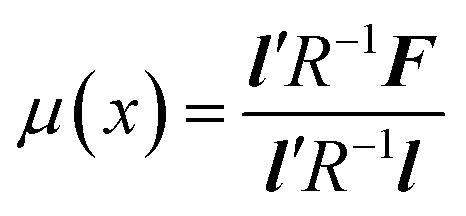
Kriging model22,23 is an expression of unknown function y as;| ŷ(x) = μ(x) + ε(x) | (1) |
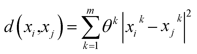 | (2) |
| Corr[Z(xi),Z(xj)] = exp(−d(xi,xj)) | (3) |
Then the kriging prediction can be expressed as;
ŷ(x) = ![[small mu, Greek, circumflex]](https://www.rsc.org/images/entities/i_char_e0b3.gif) (x) + rTR−1(F − (x) + rTR−1(F − ![[small mu, Greek, circumflex]](https://www.rsc.org/images/entities/b_i_char_e0b3.gif) ) )
| (4) |
| ri(x) = Corr[Z(x),Z(xi)] | (5) |
The unknown parameter, θ for the kriging model can be estimated by finding the maximum likelihood estimation (MLE):
 | (6) |
MLE is an m-dimensional unconstrained non-linear optimization problem. In this paper, a genetic algorithm (NSGA-II) is used to solve this problem. For a given θ, σ2 can be defined as;
 | (7) |
Then, μ(x) is assumed to be a constant value in the original kriging as;
 | (8) |
Nondominated sorting genetic algorithm-II (NSGA-II)
GA24–26 is a stochastic search method using the genetic operators, e.g., the selection, crossover and mutation. (Fig. S1 in ESI† shows the algorithms of simple GA.) In this work, the Non-dominated Sorting Genetic Algorithm-II (NSGA-II)30,31 was selected to search the minimum mass and stress of structure. NSGA-II is widely employed to solve the multi-objective optimization problem. NSGA-II is characterized by non-dominated points and crowding distance sorting. The individuals of the next generation are selected by elitism. The new generation is sequentially filled by each front until the population size exceeds the current population size (shown in ESI Fig. S2†). In this work, the blended crossover-0.5 (BLX-0.5) and the simple mutation were also applied.Screening via Latin-hypercube sampling
To design the experiment, we focused on two parameters as dominant parameters. The first parameter is the thickness of perovskite layer, which can be controlled by spin-speed for depositing PbI2 layer. The second parameter is dipping time of PbI2 thin film in MAI solution. Other possible parameters in the perovskite layer are as follows; duration time of spin coating, annealing temperature, and environmental humidity. To randomly choose the parameters, we utilized LHS method.20,21 The set of conditions was selected following the LHS as Table 1. The LHS method is one of the techniques for random value sampling that has large diversity.| Condition | Spin speed (rpm) | Dipping time (s) |
|---|---|---|
| 1 | 3580 | 712 |
| 2 | 3810 | 447 |
| 3 | 2314 | 514 |
| 4 | 4152 | 378 |
| 5 | 3336 | 402 |
| 6 | 2208 | 644 |
| 7 | 2824 | 510 |
| 8 | 3242 | 748 |
| 9 | 4430 | 492 |
| 10 | 4738 | 320 |
| 11 | 2726 | 602 |
| 12 | 4794 | 674 |
After DoE process, an ordinary kriging interpolation method22,23 was used to predict their output function from the data generated through DoE. The outputs of this experiment are fill factor (FF), short circuit current density (Jsc), open circuit voltage (Voc) and power conversion efficiency (PCE).
Next, the genetic algorithm with NSGA-II30,31 was used to investigate the best condition by finding the maximum values of FF, Jsc and Voc. In this process, the number of population was 50 and number of generation was 500. The algorithm of our optimization process is shown in ESI Fig. S3.† The optimization problem can be written as follows;
Maximize: f1 = FF
Maximize: f2 = Jsc
Maximize: f3 = Voc
Subject to: 2000 ≤ spin speed ≤ 5000, 300 s ≤ dipping time ≤ 780 s.
Result and discussion
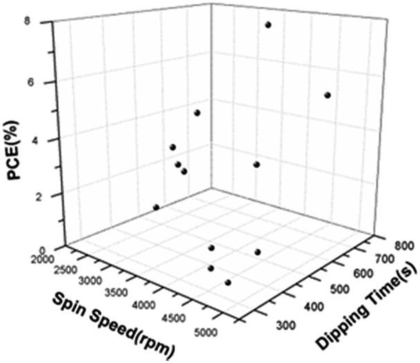
One of the important parameters to control the efficiency of solar cell is the film thickness of perovskite layers. Fig. S4† shows the relation between film thickness of perovskite layer fabricated on SnO2 layer and spin speed. We used conditions determined by LHS model (Table 1) for this measurement. One can easily see the spin speed is uniformly distributed through the whole range, which is one of the benefits of DoE based on LHS. The film thickness was decreased from 630 nm at 2314 rpm to 125 nm at 4794 rpm. From this graph, we can obtain the relationship between thickness and spin-speed by;| L = 3.05 × 10⁹/x2 | (9) |
Photovoltaic characteristics
Table 2 shows the output parameters of PVSCs fabricated using the conditions in Table 1. From Table 2, we plotted the relationship between Jsc and Voc in Fig. 2. From the original current density–voltage graph, we calculated fill factor (FF), Jsc and Voc. The conventional efficiency of solar cell can be calculated by the equation as follows;| PCE = Jsc × Voc × FF | (10) |
| Condition | Output | |||
|---|---|---|---|---|
| Jsc (mA cm−2) | Voc (V) | FF | PCE (%) | |
| 1 | 14.92 | 1.03 | 0.49 | 7.57 |
| 2 | 4.41 | 0.19 | 0.28 | 0.23 |
| 3 | 3.60 | 0.34 | 0.42 | 0.51 |
| 4 | 0.65 | 0.31 | 0.42 | 0.08 |
| 5 | 11.02 | 0.84 | 0.41 | 3.81 |
| 6 | 3.14 | 0.99 | 0.46 | 1.44 |
| 7 | 10.28 | 0.75 | 0.33 | 2.54 |
| 8 | 5.43 | 0.84 | 0.42 | 1.90 |
| 9 | 1.98 | 0.42 | 0.35 | 0.29 |
| 10 | 2.32 | 0.48 | 0.32 | 0.36 |
| 11 | 11.25 | 0.96 | 0.39 | 4.22 |
| 12 | 15.71 | 0.90 | 0.38 | 5.47 |
 | ||
| Fig. 2 Relationship between experimental parameters and efficiency of devices from original experimental data. | ||
This means that in this experiment, we optimized the efficiency by optimizing the output composed of three sub-outputs: Jsc, Voc, and FF.
From data from Table 2, the range of Jsc was from 0.1 to 15.71 mA cm−2, Voc from 0.19 to 1.03 V and FF from 0.28 to 0.49. According to low range of FF variance when compared with those of Jsc and Voc, the FF was ignored for optimization here. Fig. S5† shows the relationship between output parameter Jsc and Voc. We observed a general population of Jsc depends on Voc, having only some data have a trading off relationship: the data in the red cycle is trading off data which have high Voc with low Jsc value.
Fig. 2 shows the relationship between input parameters and efficiency from original experimental data. We observed the large difference in efficiency when we change the spin-speed and dipping time, so these input parameters are effective for finding the optimum point of the experiment. To explain the high range of efficiency difference, we have characterized the surface morphology and crystalline quality of perovskite layer, which is explained in the next part.
Surface morphology and crystalline property
The surface morphology of perovskite layer fabricated under conditions in Table 1 is shown in ESI Fig. S6.† This figure shows the difference of roughness and grain size of perovskite with PbI2 spin-speed and MAI dipping time. We observed the high roughness of perovskite in the case of low spin speed and smooth surface in the case of high-spin rate coating of PbI2. For improving the efficiency of solar cell, the low roughness of perovskite and large grain size are required.32Fig. 3(a) shows the relationship between average grain size of surface perovskite thin film fabricated by spin coating and input parameter. This graph was plotted by using analysis data of grain size average from SEM images, which is shown in ESI (Fig. S7†). We found the grain size of thin film is larger when fabricated at low spin speed. This large grain size occurs from high film thickness. Usually, large grain size has benefit to increase the efficiency,33 however in this report we could not observe the high efficiency at low spin speed, which can be explained by poor homogeneity of grain size distribution.34
 | ||
| Fig. 3 Relationship between input parameters and (a) the average grain size, (b) standard deviation and (c) crystalline conversion ratio into MAPbI3. | ||
Fig. 3(b) shows the standard deviation of the grain size of surface perovskite film and input parameters. We observed the high S.D. value when we fabricated perovskite thin film at low spin speed. This can explain the poor uniformity of grains and high roughness of the thin film. Some previous reports concluded the similar tendency that the high roughness of thin film makes the efficiency of solar cell drop.35,36
To investigate the crystalline property of perovskite layer for each condition, we measured the XRD spectra. The XRD results are shown in Fig. 4. In previous reports, the ratio of PbI2 and perovskite peak strength can explain the crystalline quality of perovskite thin film. Hsieh et al. defined the conversion ratio of PbI2 into methylammonium lead iodide (MAPbI3) with following equation;37
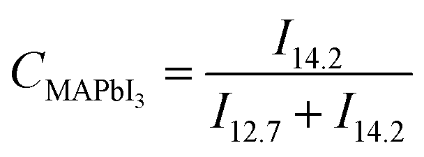 | (11) |
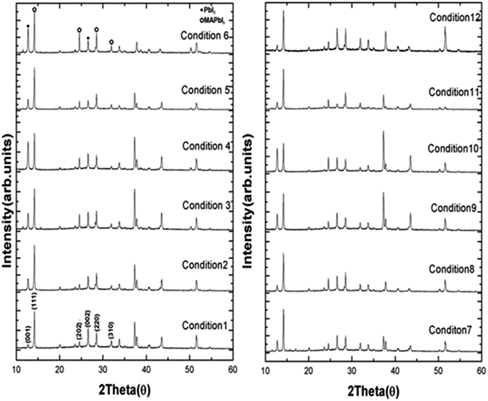 | ||
| Fig. 4 The XRD spectra of perovskite layer on FTO/SnO2 fabricated under conditions in Table 1. | ||
Fig. 3(c) shows the relationship between each experimental input parameters (spin-speed and dipping time) and CMAPbI2. We observed the low CMAPbI2 in case of low spin rate, which shows incomplete crystalline conversion due to thick PbI2 film or short contact time to MAI solution.
Predicting the mapping surface via kriging model
For using kriging model, we used output parameters from Table 2. The results of computational optimization by the kriging model are shown in Fig. 5. This figure shows the simulation of output surface distribution Jsc, Voc and power conversion efficiency (PCE). From these surface plots, we can approximate the reasonable region of input parameters for reaching the high value of output. | ||
| Fig. 5 Surface plot of the relationship between experimental parameters (spin speed, time) and outputs (a) short circuit current density (Jsc), (b) open circuit voltage (Voc) and (c) power conversion efficiency. | ||
From Fig. 5(a), we approximated the region for getting high Jsc output, Jsc higher than 12 mA cm−2, as 3400–3600, 4600–4800 rpm for spin speed and 600–740 s for dipping time. For Voc, higher than 0.9 V, the region was approximated as 2200–3800 rpm and 600–720 s (Fig. 5(b)). And for power conversion efficiency, we define the local maximum area 1 as a red color cycle, area 2 as a black color cycle and area 3 as a brown color cycle (Fig. 5(c)).
Validation of the optimization via genetic algorithm (NSGA-II)
To check our best fabrication condition, we used NSGA-II, which predicts the best condition in a different manner. Fig. S8 from ESI† shows the non-dominated solution of output parameters; Voc and Jsc; this graph is obtained by NSGA-II simulation from random best region data along Jsc and Voc in Fig. 4(a) and (b). From this graph, the predicted highest Jsc from this system is around 15.8 mA cm−2 and Voc around 1.03 V. The region for high efficiency of solar cell is obtained as Jsc around 14.8 mA cm−2 to 15.8 mA cm−2 and Voc from 0.8 to 1.05 V.To understand the two group of data, the data from area 1 and 2 from Fig. 5(c), we analyzed the SEM image, XRD data and used kriging modeling for simulating the surface of conversion of MAPbI3 and S.D. value: we already explained in the S.D. value are related to homogeneous of perovskite thin film in SEM characterization part. Fig. 6(a) shows the kriging surface of S.D. value of perovskite grains, on which lower value shows higher uniformity. Fig. 6(b) show kriging surface of conversion ratio into MAPbI3. We found that high uniformity and high conversion of MAPbI3 are important to get the high efficiency of the solar cell; the conversion of MAPbI3 has the high effect to efficiency than uniformity of perovskite thin film.
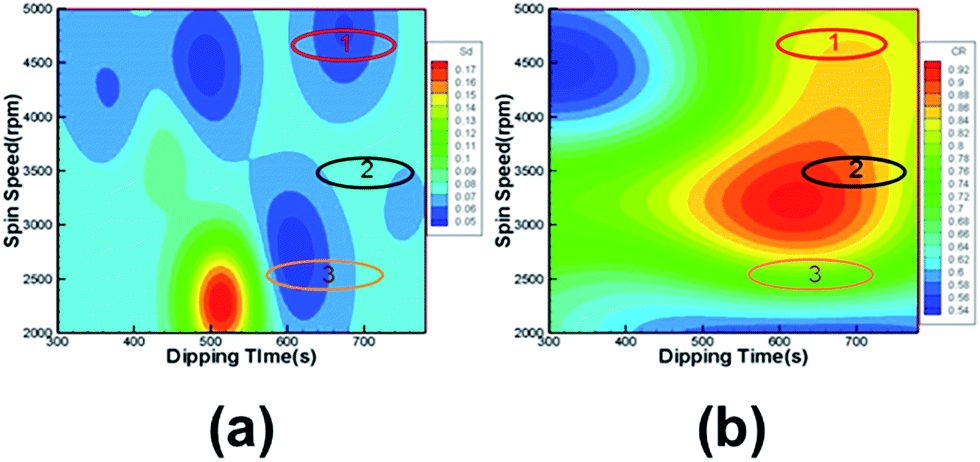 | ||
| Fig. 6 Surface plot of the relationship between experimental parameters (spin speed, time) and (a) S.D. of grain size and (b) conversion ratio of MAPbI3. | ||
Fig. 7 shows the relationship between efficiency and input parameters (spin speed and dipping time). The efficiency from this graph comes from the simulation result of FF, Jsc, and Voc. To search the global optimum condition, we chose the best condition point (data group 2) at spin-coating rate vary from 3600 rpm and dipping time around 690–720 s. The optimum area of data set come from data group 1 and data group 2. The reason to have 2 group of data is the trading-off effect between film homogeneous and high conversion of MAPbI3.
 | ||
| Fig. 7 The relationship of efficiency and input parameters (spin speed and dipping time) derived from NSGA-II. | ||
Through this computational optimization, we chose the best condition as spin-speed at 3600 rpm and dipping time at 710 s. We made 6 devices under this condition and evaluated the device performance. The average efficiency under this condition is 8.04% with standard derivation of 0.42, and average Jsc = 15.51 mA cm−2, Voc = 1.03 V and FF = 0.51. The full data of each device is shown in ESI (Table S2†). The maximum PCE of this experiment was 8.87% with Jsc = 16.56 mA cm−2, Voc = 1.03 V and FF = 0.52, whose graph of the current–voltage characteristic is shown in ESI Fig. S9.† It is notable that all the optimization process was done only through 18 samples in total even though we have two experimental parameters with 12 levels, which ordinary means that 212 = 4096 of samples are required for obtaining full information of the system. This improvement comes from (1) highly effective sampling of LHS method, (2) high accuracy of kriging method for a few data sets, and (3) high effectiveness of NSGA-II for selecting the best point from kriging result.
Conclusions
In conclusion, we have successfully fabricated PVSCs with structure FTO/SnO2/perovskite/spiro-OMeTAD/Au. This structure is a good candidate for flexible devices with low-cost material. To find the maximum efficiency, we optimized the experimental conditions using the kriging model method from experimental data given through Latin hypercube sampling. With only 12 conditions of experiments, we could approximate the best condition for fabricating PVSCs as the spin speed 3600 rpm and dipping time 710 s. Under this condition, we observed a high efficiency of PVSCs at 8.87% (Jsc = 16.56 mA cm−2, Voc = 1.03 V, FF = 0.52). From the LHS and mapping surface by Kriging, we could observe that the spin-coating speed and MAI dipping time have strong relationships with efficiency due to the conversion ratio of PbI2 to MAPbI3 and the surface morphology of the perovskite film. This optimization method will allow researchers to go much faster through a variety of system in PVSCs.Conflict of interest
The authors declare no competing financial interest.Acknowledgements
The author Atthaporn Ariyarit thanks to the financial support of Ministry of Education, Culture, Sports, Science and Technology (MEXT), Japan. We are deeply grateful to Atthaphon Ariyarit from Tokyo metropolitan university who provided considered feedback and insightful comments for simulation process.Notes and references
- P. Docampo, J. M. Ball, M. Darwich, G. E. Eperon and H. J. Snaith, Nat. Commun., 2013, 4, 1–6 CrossRef PubMed.
- J. M. Ball, M. M. Lee, A. Hey and H. J. Snaith, Energy Environ. Sci., 2013, 6(6), 1739–1743 CAS.
- M. H. Kumar, N. Yantara, S. Dharani, M. Graetzel, S. Mhaisalkar, P. P. Boix and N. Mathews, Chem. Commun., 2013, 49(94), 11089–11091 RSC.
- H. S. Kim, J. W. Lee, N. Yantara, P. P. Boix, S. A. Kulkarni, S. Mhaisalkar, M. Grätzel and N. G. Park, Nano Lett., 2013, 13(6), 2412–2417 CrossRef CAS PubMed.
- C. S. Ponseca Jr, T. J. Savenije, M. Abdellah, K. Zheng, A. Yartsev, T. Pascher, T. Harlang, T. Chabera, T. Pullerits, A. Stepanov and J. P. Wolf, J. Am. Chem. Soc., 2014, 136(14), 5189–5192 CrossRef PubMed.
- M. Saliba, T. Matsui, J. Y. Seo, K. Domanski, J. P. Correa-Baena, M. K. Nazeeruddin, S. M. Zakeeruddin, W. Tress, A. Abate, A. Hagfeldt and M. Grätzel, Energy Environ. Sci., 2016, 9(6), 1989–1997 CAS.
- Q. Chen, H. Zhou, Z. Hong, S. Luo, H. S. Duan, H. H. Wang, Y. Liu, G. Li and Y. Yang, J. Am. Chem. Soc., 2013, 136(2), 622–625 CrossRef PubMed.
- Q. Wang, Y. Shao, Q. Dong, Z. Xiao, Y. Yuan and J. Huang, Energy Environ. Sci., 2014, 7(7), 2359–2365 CAS.
- Q. Lin, A. Armin, R. C. R. Nagiri, P. L. Burn and P. Meredith, Nat. Photonics, 2015, 9(2), 106–112 CrossRef CAS.
- C. Huang, W. Fu, C. Z. Li, Z. Zhang, W. Qiu, M. Shi, P. Heremans, A. K.-Y. Jen and H. Chen, J. Am. Chem. Soc., 2016, 138, 2528–2531 CrossRef CAS PubMed.
- A. Agresti, S. Pescetelli, L. Cinà, D. Konios, G. Kakavelakis, E. Kymakis and A. D. Carlo, Adv. Funct. Mater., 2016, 26, 2686–2694 CrossRef CAS.
- K. Wojciechowski, T. Leijtens, S. Spirova, C. Schlueter, M. Hoerantner, J. T.-W. Wang, C.-Z. Li, A. K.-Y. Jen, T.-L. Lee and H. J. Snaith, J. Phys. Chem. Lett., 2015, 6, 2399–2405 CrossRef CAS PubMed.
- N. Vaenas, D. Konios, T. Stergiopoulos and E. Kymakis, RSC Adv., 2015, 5, 107771–117776 RSC.
- G. E. Eperon, V. M. Burlakov, A. Goriely and H. J. Snaith, ACS Nano, 2013, 8(1), 591–598 CrossRef PubMed.
- H. S. Kim and N. G. Park, J. Phys. Chem. Lett., 2014, 5(17), 2927–2934 CrossRef CAS PubMed.
- T. A. Ngo, J. Kim and S. S. Kim, J. Ind. Eng. Chem., 2013, 19(1), 137–143 CrossRef CAS.
- M. I. Beser, J. Beltrán and V. Yusà, J. Chromatogr. A, 2014, 1323, 1–10 CrossRef CAS PubMed.
- M. J. Chen, K. N. Chen and C. W. Lin, J. Food Eng., 2005, 68(4), 471–480 CrossRef.
- R. Bashiri, N. M. Mohamed, C. F. Kait, S. Sufian and H. Hanaei, Procedia Eng., 2016, 148, 151–157 CrossRef CAS.
- B. Minasny and A. B. McBratney, Comput. Geosci., 2006, 32(9), 1378–1388 CrossRef.
- N. Pholdee and S. Bureerat, Int. J. Syst. Sci., 2015, 46(10), 1780–1789 CrossRef.
- L. Teixeira and A. O. Falcao, Inf. Model. Model., 2014, 54(7), 1833–1849 CrossRef PubMed.
- Y. Gao and X. Wang, Int. J. Adv. Des. Manuf. Technol., 2008, 37(9), 953–960 CrossRef.
- A. Ariyarit and M. Kanazaki, J. Mech. Sci. Tech., 2015, 29(4), 1443–1448 CrossRef.
- J. Horn, N. Nafpliotis and D. E. Goldberg, IEEE World Congress on Computational Intelligence, Proceedings of the First IEEE Conference on, IEEE, 1994, pp. 82–87 Search PubMed.
- G. Jones, P. Willett, R. C. Glen, A. R. Leach and R. Taylor, J. Mol. Biol., 1997, 267(3), 727–748 CrossRef CAS PubMed.
- Y. Zhang, M. Liu, G. E. Eperon, T. C. Leijtens, D. McMeekin, M. Saliba, W. Zhang, M. Bastiani, A. Petrozza, L. M. Herz, M. B. Johnston, H. Lin and H. J. Snaith, Mater. Horiz., 2015, 2(3), 315–322 RSC.
- E. Mosconi and F. D. Angelis, ACS Energy Lett., 2016, 1(1), 182–188 CrossRef CAS.
- H. S. Kim, C. R. Lee, J. H. Im, K. B. Lee, T. Moehl, A. Marchioro, S. J. Moon, R. Humphry-Baker, J. H. Yum, J. E. Moser, M. Grätzel and N. G. Park, Sci. Rep., 2012, 2, 591 Search PubMed.
- H. Li and Q. Zhang, IEEE. Trans. Evol. Comput., 2009, 13(2), 284–302 CrossRef.
- K. Deb, A. Pratap, S. Agarwal and T. Meyarivan, IEEE. Trans. Evol. Comput., 2002, 6(2), 182–197 CrossRef.
- C. Zuo and L. Ding, Nanoscale, 2014, 6(17), 9935–9938 RSC.
- W. Nie, H. Tsai, R. Asadpour, J. C. Blancon, A. J. Neukirch, G. Gupta, J. J. Crochet, M. Chhowalla, S. Tretiak, M. A. Alam and H. L. Wang, Science, 2015, 347(6221), 522–525 CrossRef CAS PubMed.
- X. Ren, Z. Yang, D. Yang, X. Zhang, D. Cui, Y. Liu, Q. Wei, H. Fan and S. F. Liu, Nanoscale, 2016, 8(6), 3816–3822 RSC.
- C. C. Chen, Z. Hong, G. Li, Q. Chen, H. Zhou and Y. Yang, J. Photonics Energy, 2015, 5(1), 057405 CrossRef.
- F. Di Giacom, S. Razza, F. Matteocci, A. D'Epifanio, S. Licoccia, T. M. Brown and A. Di Carlo, J. Power Sources, 2014, 251, 152–156 CrossRef.
- T. Y. Hsieh, T. C. Wei, K. L. Wu, M. Ikegami and T. Miyasaka, Chem. Commun., 2015, 51(68), 13294–13297 RSC.
Footnote |
| † Electronic supplementary information (ESI) available. See DOI: 10.1039/c6ra20956d |
| This journal is © The Royal Society of Chemistry 2016 |