
 Open Access Article
 This Open Access Article is licensed under a Creative Commons Attribution-Non Commercial 3.0 Unported Licence
The properties, photovoltaic performance and stability of visible to near-IR all inorganic perovskites†
Adva
Shpatz Dayan
a,
Xinjue
Zhong
 b,
Małgorzata
Wierzbowska
c,
C. E. M.
de Oliveira
d,
Antoine
Kahn
b and
Lioz
Etgar
*a
b,
Małgorzata
Wierzbowska
c,
C. E. M.
de Oliveira
d,
Antoine
Kahn
b and
Lioz
Etgar
*a
aInstitute of Chemistry, Casali Center for Applied Chemistry, The Hebrew University of Jerusalem, Jerusalem 91904, Israel. E-mail: lioz.etgar@mail.huji.ac.il
bDepartment of Electrical Engineering, Princeton University, Princeton, New Jersey 08544, USA
cInstitute of High Pressure Physics, Polish Academy of Sciences Sokołowska 29/37, 01-142 Warsaw, Poland
dThe Center for Nanoscience and Nanotechnology, The Hebrew University of Jerusalem, Jerusalem 91904, Israel
First published on 28th July 2020
Abstract
Hybrid metal halide perovskites have seen an exponential increase in the scientific community due to their successful introduction in solar cells. However, these materials are known to suffer from thermal instability, toxicity and limited absorption range. One way to overcome these obstacles is by substituting the organic cation with an inorganic one and by replacing the lead with tin, which can shift the absorbance to the near infra-red (NIR). In this work we synthesized several compositions of all inorganic CsSnyPb1−yBrxI3−x (0 ≤ y ≤ 1, 0 ≤ x ≤ 3) perovskites, achieving a wide band gap range from 1.3 eV to 1.75 eV. It was found that Sn stabilizes the CsPbI3 black photovoltaic (PV) active phase and at the same time shifts the absorbance to the NIR. Although some of these perovskite compositions are already known, here we analyzed in detail their physical and electronic properties. Hall effect measurements show an increase in the carrier concentration and Hall mobility with the addition of Sn. Interestingly, the Hall mobility is five times higher for CsSnI3 than in the case of having just 10% Pb and 90% Sn in the perovskite structure. Ultraviolet photoemission spectroscopy (UPS) and density functional theory (DFT) calculations reveal the energy level position and phase mixing, which explain the reduction in the photovoltaic performance with the addition of Sn. The best PV performance of 12.7% efficiency was achieved in the case of an 80![[thin space (1/6-em)]](https://www.rsc.org/images/entities/char_2009.gif) :20 Pb:Sn ratio, which is one of the highest PCEs reported for similar perovskite compositions.
:20 Pb:Sn ratio, which is one of the highest PCEs reported for similar perovskite compositions.
1. Introduction
Organic–inorganic perovskites are being used today in a variety of optoelectronic applications. Hybrid perovskites have several unique properties which make them attractive semiconductors for use in the photovoltaic (PV) field.1–3 In order for the perovskite to function efficiently as a light harvester in the solar cell, it must be stable under environmental conditions (especially moisture)4–6 and have high photostability for long term use.7–9The general formula of basic halide perovskites is ABX3 where A is generally an organic cation (methylammonium – MA+, formamidinium – FA+) but can be also an inorganic cation (Cs+); B is a divalent metal cation (Pb2+, Sn2+,Ge2+, Sr2+, and Cu2+)10–13 and X is a halide anion (Cl−, Br−, I−).
The common hybrid perovskite used in solar cells over the past few years is CH3NH3PbI3 (MAPbI3). However, this material has an organic cation (usually MA+) which makes the entire structure relatively unstable under high temperature.14–16 Moreover, the use of Pb as the divalent cation is problematic due to its toxicity.17–19 Several reports show that the replacement of the organic cation by an inorganic cation can improve the stability of the perovskite.20–26 Following this direction, one of the potential candidates is CsPbI3, which has an absorbance onset around 700 nm. CsPbI3 has four phases: α, β, γ and δ, but only α and β can be used in PV solar cells, while γ and δ are metastable phases that are inactive in PV cells.27 The transition between the phases usually happens due to exposure to air when the α phase, which is cubic, transforms to the β phase (tetragonal structure) and then to the γ and δ phases (orthorhombic structure). In our previous report, we showed that CsPbI3 can be stabilized in a two dimensional structure (2D);28 however, it forms a wide band gap, which makes it problematic to function efficiently in a solar cell.29 Other methods to stabilize the CsPbI3 active phase include the addition of different salts such as EuBr2, EuCl2, and CaI2.25–31
Modifying the B site in CsPbI3 can tune the optical properties and at the same time can enhance its stability. The replacement of lead (Pb) by tin (Sn) in the case of MA+ based perovskites leads to a variation in the band gap from 1.55 eV for MAPbI3 to 1.3 eV for MASnI3.32–35 Replacing Pb with Sn in the case of a fully inorganic perovskite (Cs based perovskite) might assist in getting a stable structure and at the same time will shift the absorbance to the near-IR. Moreover, introducing Sn instead of Pb will reduce the toxicity of the perovskite.
In order for another element to be able to replace Pb2+ in the perovskite structure, it needs to have a coordination number equal to six and a similar ionic radius. An additional indication can be obtained from the Goldschmidt tolerance factor (eqn (1)), where rA is the radius of the A cation, rB is the radius of the B cation, and rX is the radius of the anion.
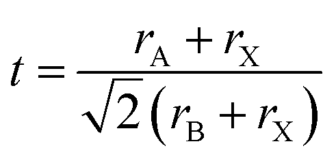 | (1) |
The ionic radius of Sn2+ is smaller than that of Pb2+;36 therefore, when introducing more Sn2+ instead of Pb2+, the tolerance factor increases and as a result we observe a perovskite which has a stable structure compared to CsPbI3.37,38 In addition, the Sn–I bond length is shorter than the Pb–I bond length, which supports a stable structure in the case of Sn-based perovskites.
The radius of the inorganic cation (Cs+) is smaller than that of MA+, which suggests further enhancement in the stability of the structure.39 CsSnI3 was demonstrated first in 2012 by Chung et al.,40 who used it as a hole transport material (HTM) in dye-sensitized solar cells.41 In 2016 Wang et al. studied CsSnI3 as the light harvester material in a solar cell and reported an efficiency of 3.31%.42 The combination of Sn and Pb in the solar cell was reported using organic cations (MA+ and FA+), achieving a power conversion efficiency (PCE) of 15%. In addition, in 2015 Sabba et al. published their work using CsSnI2.9Br0.1 as a light harvester material in a solar cell and achieved a low PCE of 1.67%.40 Other reports demonstrate the use of bromide and mixed halides with solely Sn in solar cells.43–45
Liu et al. synthesized CsSn1−xPbxI3 and CsSn1−xPbxBr2I nanocrystals and used them in light emitting diode devices.46 In 2017 Liang et al. used all inorganic perovskites with mixed halides (Br, I).47 In this study they used CsPbBr3, CsPbIBr2 and a specific composition CsPb0.9Sn0.1IBr2 (where the amount of Sn is no more than 10%), and demonstrated a PCE of 11.33%. A year later Li et al. used the CsPb0.75Sn0.25IBr2 perovskite (keeping the ratio between the halides constant), achieving a slightly higher PCE of 11.53%.48
Although these compositions were already discussed in the literature, here we shed light on their physical, stability and electronic properties using Hall effect measurements and ultraviolet photoelectron spectroscopy (UPS). We combine an inorganic cation (i.e. Cs+) with Pb and Sn at the B site of the perovskite. We synthesize and study materials using various ratios of Sn and Pb based on the chemical formula CsSnyPb1−yBrxI3−x (Table 1). As a result we were able to achieve a wide range of band gaps from 1.3 eV to 1.75 eV. The Hall effect and UPS measurements reveal the hole mobility, carrier density and the energy level position of this fully inorganic perovskite. The stability under humidity and photostability of these compositions as films and full devices are also studied. Finally, we demonstrate the application of these compositions in mesoporous perovskite based solar cells, achieving one of the highest efficiencies reported for CsSnyPb1−yBrxI3−x perovskites.
| Pb:Sn ratio |
Perovskite composition |
|---|---|
| 100:0 |
CsPbI3 |
| 90:10 |
CsSn0.1Pb0.9I2.8Br0.2 |
| 80:20 |
CsSn0.2Pb0.8I2.6Br0.4 |
| 70:30 |
CsSn0.3Pb0.7I2.4Br0.6 |
| 60:40 |
CsSn0.4Pb0.6I2.2Br0.8 |
| 50:50 |
CsSn0.5Pb0.5I2Br1 |
| 40:60 |
CsSn0.6Pb0.4I1.8Br1.2 |
| 30:70 |
CsSn0.7Pb0.3I1.6Br1.4 |
| 20:80 |
CsSn0.8Pb0.2I1.4Br1.6 |
| 10:90 |
CsSn0.9Pb0.1I1.2Br1.8 |
| 0:100 |
CsSnI3 |
2. Results and discussion
Introducing Sn (instead of Pb) into the perovskite structure can lead to four different phases, as in the case of CsPbI3, with some of them being PV active. Since Cs+ is used as the cation, it occupies the 1b Wyckoff position in the center of the perovskite cube, and therefore it is easier to create the ideal cubic Pm![[3 with combining macron]](https://www.rsc.org/images/entities/char_0033_0304.gif) m structure than in the case of most organic cations.
m structure than in the case of most organic cations.
Our motivation here was to find a way to stabilize the active CsPbI3 phase. Here we used the Sn2+ cation in addition to the Pb2+ cation in order to create a good overlap between the orbitals of the divalent metal cation (Pb2+ and Sn2+) and the orbitals of the halide anion (I−, Br−). The band gap of these semiconductors is determined by the orbitals of the halide and the divalent metal cation.49 It is known that the valence-band maximum (VBM) is predominantly determined by the anti-bonding component of the hybridization between the divalent metal in the B site and the halide in the X site, while the conduction-band minimum (CBM) is dominated by the nonbonding component of the divalent metal. In the case of Pb halides, the overlap of Pb–I/Br is between the 6s orbital of Pb2+ and the 5p or 4p orbital of I− or Br−, respectively. The 6s and 6p orbitals of Pb are at a higher binding energy compared to the 5s and 5p orbitals of Sn, and as a result the binding energy of the s–p hybridized antibonding levels is lower for Sn (5s) and (5p)–X(p) than for Pb(6s) and (6p)–X(p). As a consequence, both the VBM and CBM undergo an upshift when Sn replaces Pb.50
Fig. 1a and b show the absorbance as a function of Sn concentration in the CsSnyPb1−yBrxI3−x perovskite structure. The absorption edge shifts to longer wavelength and extends to the Near Infra-Red (NIR) region with increasing Sn concentration. Similar bandgap changes have been observed in MASnxPb1−xI3.32
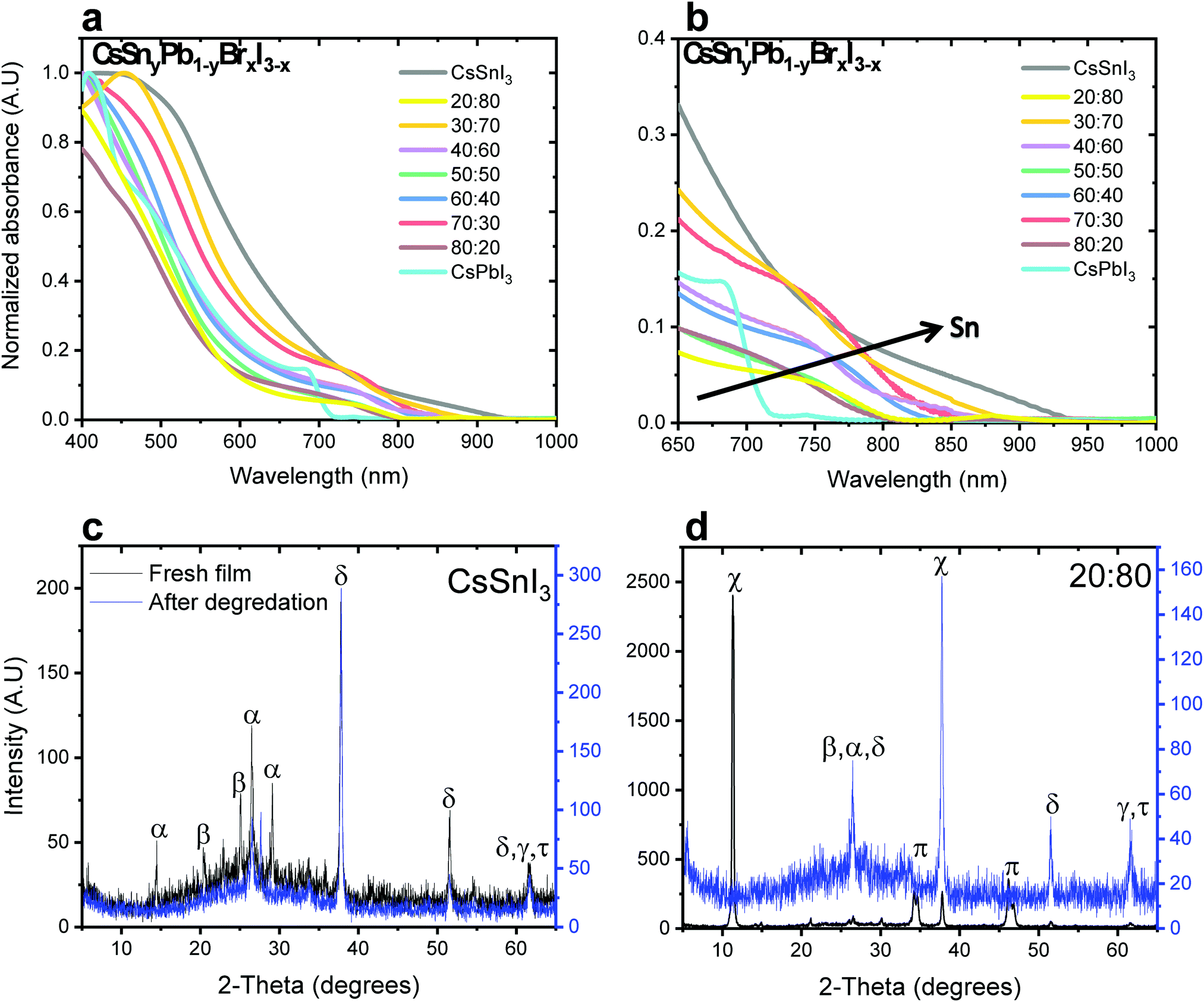 | ||
| Fig. 1 (a) Absorbance spectra of CsSnyPb1−yBrxI3−x (0 ≤ y ≤ 1, 0 ≤ x ≤ 3) films encapsulated at different ratios of Pb:Sn. (b) Magnification of the absorbance spectra (shown in (a)) in the range of 650–1000 nm. XRD patterns of (c) CsSnI3 and (d) CsSn0.8 Pb0.2 I1.4Br1.6 (Pb:Sn – 20:80) before and after degradation. (π – CsPbI3 cubic phase, χ – CsPbI3 orthorhombic phase, α – CsSnI3, δ – SnO2, β – SnI2, γ – PbI2, τ – CsI.) | ||
In order to compare the influence of the B site (i.e. Sn vs. Pb) to that of the X site (i.e. I vs. Br) on the optical properties, we synthesized CsSnyPb1−yI3 and CsSnyPb1−yBrxI3−x (0 ≤ y ≤ 1, 0 ≤ x ≤ 3). In the synthesis of CsSnyPb1−yBrxI3−x the bromide has one source, i.e., SnBr2, whereas the iodide has two sources, PbI2 and CsI.
Fig. 2a shows the band gap as a function of the Pb:Sn ratios in both cases of mixed bromide–iodide and pure iodide. As was discussed above, the band gap decreases with the addition of Sn. Moreover, the influence of the bromide on the band gap is also observed. The change in the band gap is more pronounced in the case of pure iodide compare to the case of mixed iodide-bromide. The bromide shifts the absorbance to shorter wavelength, which compensates slightly for the red shift due to the addition of Sn. This can be explained when looking at the slope of the curves in Fig. 2a. The slope of the green dots (pure iodide) is larger by 1.5 times than the slope of the blue dots (mixed bromide–iodide). All the absorbance spectra can be seen in Fig. S1 and S3 (ESI†). Therefore, we can suggest that the influence of Sn on the band gap is more pronounced than that of bromide in this case. We were able to achieve a wide range of band gaps from 1.3 eV to 1.75 eV.
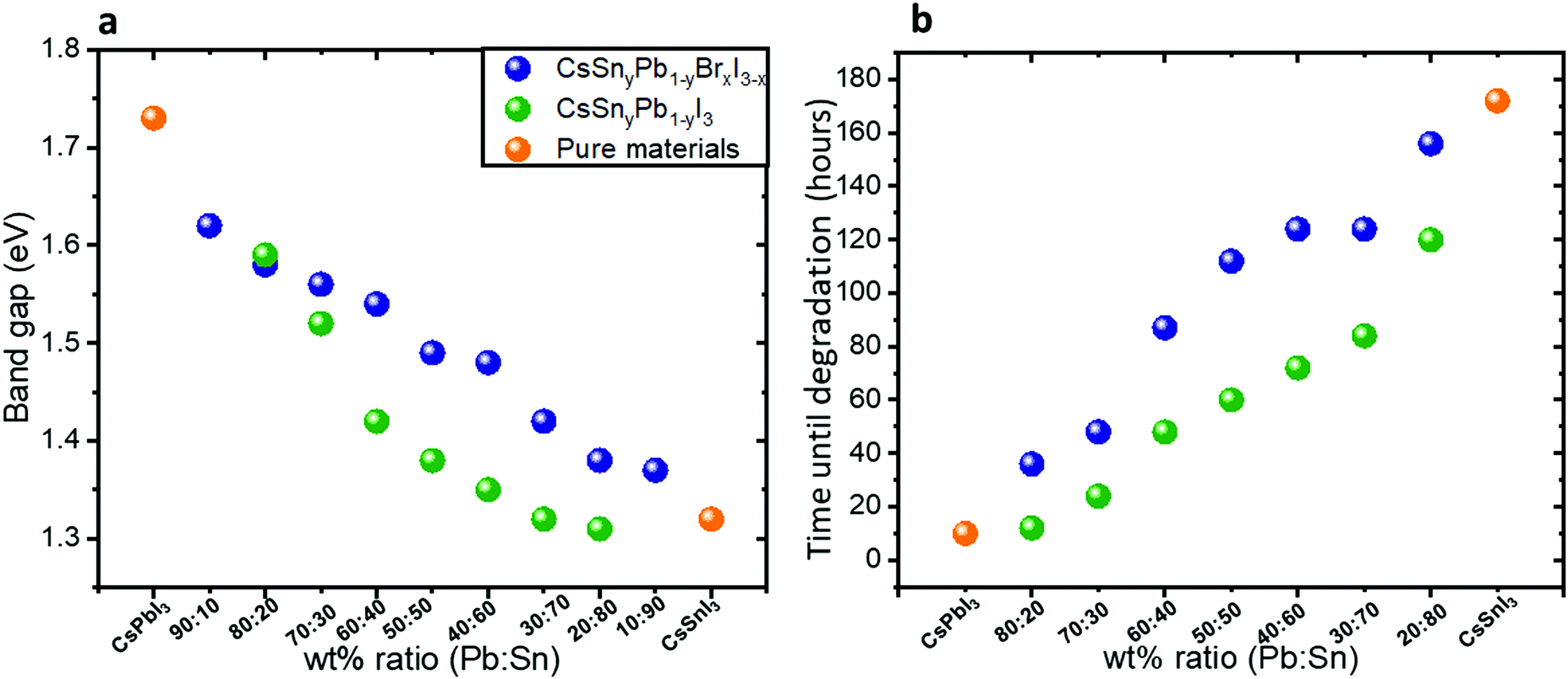 | ||
| Fig. 2 (a) The band gap as a function of the Pb:Sn ratio for the cases of mixed iodide and bromide and for pure iodide compounds. The slope of the green dots is 1.5 times larger than the slope of the blue dots. (b) Photostability measurements under 1 sun illumination, 18 °C and 27% humidity. The data in this graph are based on the absorbance spectra shown in Fig. S4 and S5 (ESI†). | ||
X-ray diffraction (XRD) measurements were performed for different ratios of Pb:Sn. Fig. 1c and d show the cases of pure CsSnI3 and CsSnyPb1−yBrxI3−x with a 20:80 Pb:Sn ratio, respectively. (Other Pb:Sn ratios are presented in the ESI,† in Fig. S2.) The black curve corresponds to the fresh film, while the blue curve corresponds to the film after degradation. In our previous work we found that after 48 hours at room conditions (ambient air) full degradation is observed.28 We determine full degradation of the perovskite by absorbance and XRD measurements, which indicate the presence of the material's precursors (mainly PbI2 and CsI). Fig. 1c exhibits peaks related to CsSnI3 (2θ = 14, 27, 29°) and SnI2 (2θ = 22, 28°), where peaks related to SnO2 (2θ = 39, 62°) can be observed just after degradation due to the Sn oxidation. The spectrum for a 20:80 Pb:Sn ratio can be seen in Fig. 1d, where the cubic and the orthorhombic phases of CsPbI3 can be observed. After degradation, the perovskite dissociates into SnI2, PbI2 and CsI. The presence of CsPbI3 in the fresh film suggests that both CsPbI3 and CsSnI3 are formed.
Photostability measurements on the synthesized hybrid CsSnyPb1−yBrxI3−x and CsSnyPb1−yI3 were performed under continuous 1 sun illumination, 18 °C and 27% humidity. Fig. 2b summarizes these measurements for different Pb:Sn ratios. For each ratio we followed the absorbance spectra as a function of time. The corresponding absorbance spectra are presented in Fig. S4 and S5 (ESI†). It can be seen clearly that as the Sn amount increases, the photostability of the perovskite increases. For example, at a Pb:Sn ratio of 20:80, the perovskite does not degrade for 172 hours under continuous 1 sun illumination, 18 °C and 27% humidity. Interestingly, even in the case of 20% Sn in the perovskite structure, the photostability improved notably compared to pure CsPbI3. An important observation from these measurements is that the mixed halide (iodide and bromide) perovskite is more photostable than the single halide (i.e. iodide) perovskite in the structure. Based on this fact, the rest of the work concentrates on the mixed halide perovskite. Scanning electron microscopy (SEM) micrographs of the films before and after degradation (48 hours) are presented in Fig. S6 (ESI†). After degradation there are more pinholes and the grain boundaries are better defined than in the case of fresh films.
Following the photostability measurements, we explored the stability of the different samples under room conditions and without encapsulation. The photographs of the films as a function of time are shown in Fig. S7 and S8 (ESI†). Similar to the case of the photostability measurements, when the ratio of Sn:Pb is higher, the perovskite is more stable in air without encapsulation. It can be seen that CsSnI3 is stable in air for over 48 hours. Similar to the photostability measurements, films with Pb:Sn ratios of 20:80, 30:70 and 40:60 showed excellent stability for over 24 hours. It is important to keep in mind that CsPbI3 cannot survive more than 10 min in air.28 These experiments (photostability and stability) indicate clearly that the resistance of the perovskite to humidity is enhanced when Pb is replaced by Sn. This enhanced stability is in contrast to the case of the perovskite with mixed Pb and Sn having an organic cation at the A site. In this case the stability decreases by more than 50% when introducing Sn into the perovskite.51 In our case (see Fig. 3), since Cs is used as the inorganic cation at the A site, the lattice parameter is reduced and the cubic structure shrinks compared to the case of an organic cation, which changes the tolerance factor, and this slows down the oxidation reaction of Sn and provides enhanced stability.51 In addition to that effect, it was found that mixed halide perovskites (iodide and bromide) have better stability than single halide (iodide) perovskites.52
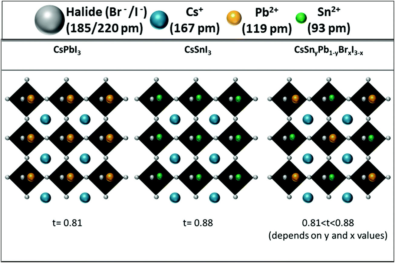 | ||
| Fig. 3 Schematic illustration of the change in the tolerance factor as a result of Cs, Pb and Sn in the perovskite structure. | ||
In order to study the hole mobility, carrier concentration and resistivity for the various Pb:Sn ratios, Hall effect measurements were performed. When a magnetic field is applied on a conductor or a semiconductor that carries an electric current, a potential difference across the sample and perpendicular to both the current and the magnetic field will be developed. This is called the Hall effect, and the potential difference developed across the sample is the Hall voltage (VH). By measuring the Hall voltage, it is possible to get the nq product, the mobile carrier density multiplied by the charge of carriers (n – electron density, q – charge of carriers). Several studies showed the use of Hall effect measurements to reveal the properties of 2D materials such as black phosphorene.53,54
Hall effect measurements were performed on perovskite films deposited on microscope glass substrates with four gold contacts at the corners. It can be observed in Fig. 4a–c that, as the amount of Sn increases, the carrier concentration and the mobility increase, while the resistivity decreases. This trend can be explained by the oxidization of Sn. It is known that Sn2+ oxidizes easily in an ambient atmosphere to Sn4+.51 The replacement of Sn2+ by Sn4+ in the perovskite structure has been linked to hole doping, which increases the number of carriers55 and can explain the decrease in resistivity as shown in Fig. 4a. As the Pb:Sn ratio increases, there is more Sn in the structure, which potentially can be oxidized, and Fig. 4 shows that the carrier concentration, hole mobility and resistivity change as a function of this ratio.
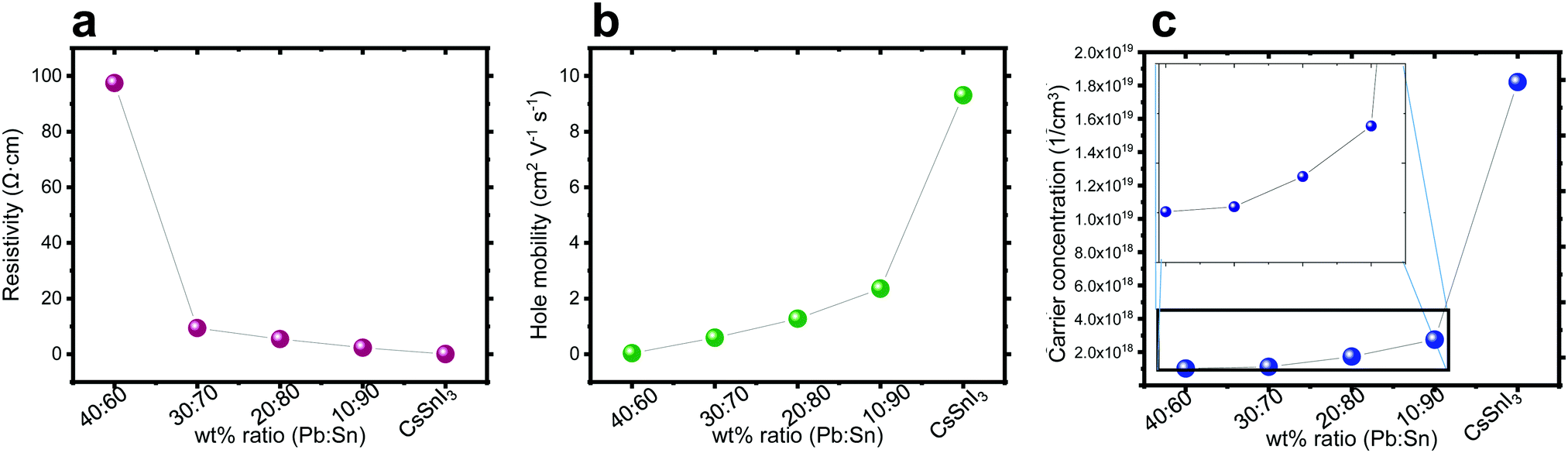 | ||
| Fig. 4 Hall effect measurement of the different ratios Pb:Sn: (a) resistivity, (b) hole mobility, and (c) carrier concentration. | ||
The carrier type determines the semiconductor type. The Hall effect measurement can assist in determining the type of these semiconductors. It was observed that with the addition of Pb into the perovskite structure the behavior of the film is becoming less p-type. In general, doping the structure with Pb influences dramatically the properties (mobility, carrier concentration and resistivity) compared to a perovskite which is solely based on Sn.
The energy levels of films with different ratios of Pb:Sn were measured by ultraviolet photoemission spectroscopy (UPS). The perovskite films were spin-coated on conductive indium tin oxide (ITO)/glass substrates. Fig. 5a and b show the photoemission cut-off and the VBM, respectively, measured on CsSn0.2Pb0.8I2.6Br0.4. The cut-off position yields a work function of 4.77 eV. The valence band spectrum, recorded and plotted on a logarithmic scale, shows the VBM at 0.89 eV below the Fermi level (0 eV on the energy scale). The ionization energy (IE) of this film (Pb:Sn – 80:20) is therefore 5.66 eV. Measurements on films with various Pb:Sn ratios show that the IE decreases to 5.64 eV for 70:30, 5.56 eV for 60:40, and finally to 5.37 eV for 20:80 (see Fig. S9, ESI†). By combining the optical bandgap and the VBM position, the position of the CBM can be estimated, assuming that the exciton binding energy is small and negligible with respect to the photoemission resolution in 3D perovskites.56–58 The CBM shifts to higher energy with increasing Sn2+ concentration, following the trend of the VBM, as shown in Fig. 5c. The IE of CsPbI3 is higher than expected, mainly due to the fast degradation of the film during sample transfer. It has been reported50,59 that the VBM arises from antibonding hybridization of Pb (6s) and/or Sn (5s) and halide (np) orbitals. The lower binding energy of the Sn 5s orbitals compared to the Pb 6s orbitals upshifts the VBM with increasing Sn content, which is consistent with the experimental results. The CBM is derived from the hybridization of the antibonding Pb (6p) and/or Sn (5p) state and the halide (np) orbitals with major contributions from Pb (6p) and/or Sn (5p). Some reports suggest that the CBM of the Pb–Sn alloy is mainly composed of Pb 6p and I 5p orbitals since the binding energy of the Sn 5p orbital is lower than that of the Pb 5p orbital.60 The addition of Sn and Br in the mixed perovskites reduces the lattice constant and thus enhances the hybridization, which pushes the CBM to higher energy.61Fig. 5d shows the experimental and calculated band gaps for the different ratios. Density functional theory (DFT) was used for the band gap calculations (see more details in the Experimental section). The experimental band gaps are in between the calculated band gaps for the cubic structure and the orthorhombic structure. It can be suggested that our different films have a mix of cubic and orthorhombic structures. For a low amount of Sn, the cubic structure is dominant, but when the Sn amount increases the orthorhombic structure (which is a metastable phase) starts to appear. Since the orthorhombic structure is inactive in solar cells, it influences the PV results as is discussed below.
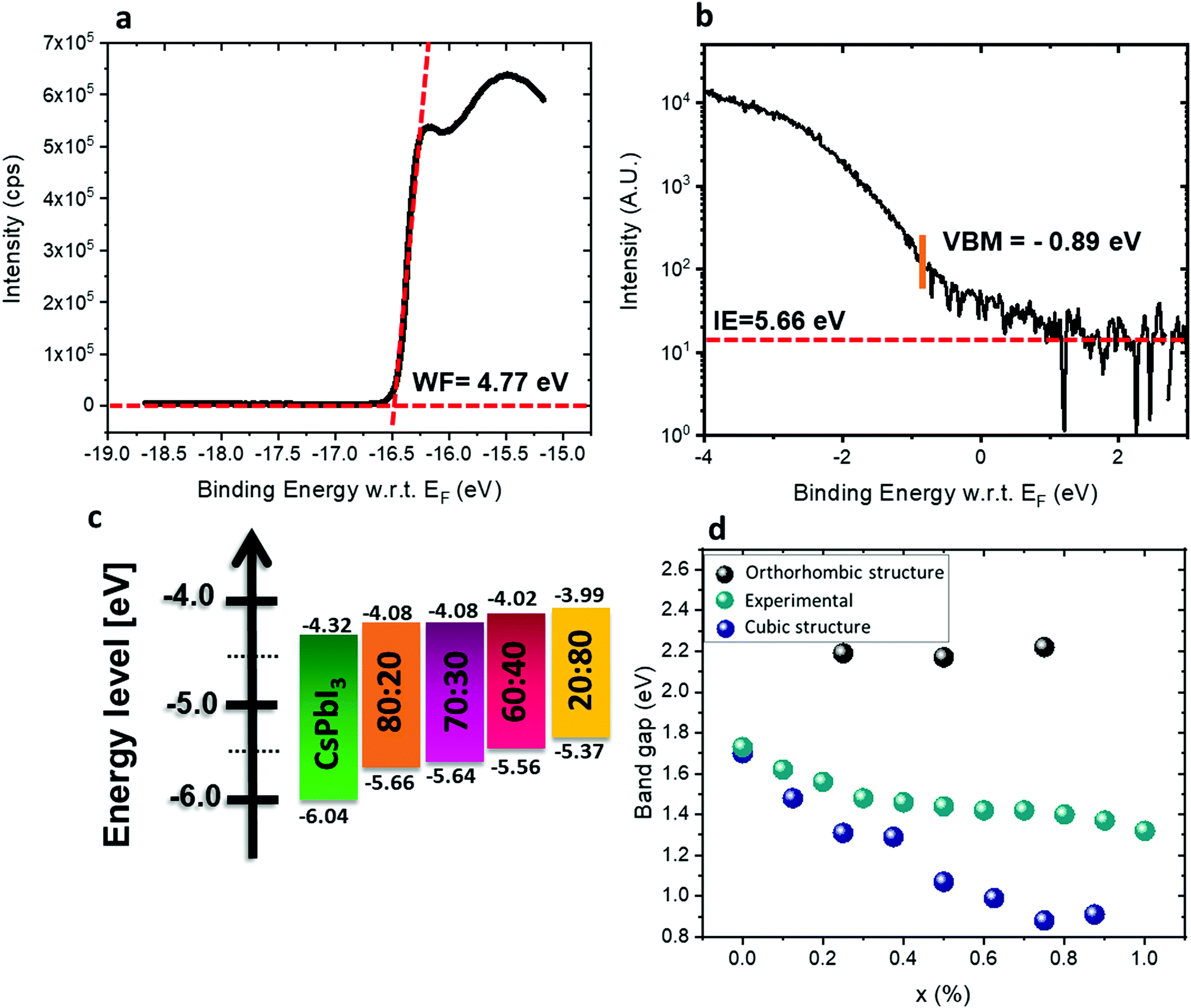 | ||
| Fig. 5 (a) Photoemission cut-off measured via UPS for CsSn0.2Pb0.8I2.6Br0.4. (b) The position of the VBM and ionization energy (IE) for CsSn0.2Pb0.8I2.6Br0.4 measured by UPS. (c) Energy diagram of the different materials used in this study. The band gap of CsPbI3 is relatively wide with respect to the literature value,62 which is due to degradation as discussed in the text. (d) Experimental results and theoretical calculation of the band gaps for the various ratios when adding SnBr2. X represents the ratio Pb:Sn. | ||
Based on our chemical and physical characterizations, we introduced several perovskites with different ratios of Pb:Sn into solar cells. We investigated three ratios of Pb:Sn – 80:20, 70:30 and 60:40 – using PTAA (poly[bis(4-phenyl)(2,4,6-trimethylphenyl)amine]) as the hole transport material, as presented in Fig. 6b. Fig. 6a shows an SEM cross section of the discussed solar cell, where the different layers can be observed clearly.
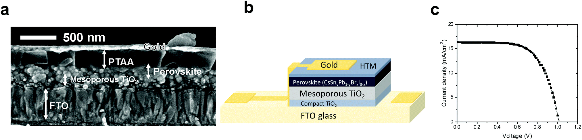 | ||
| Fig. 6 (a) Cross section SEM image of the PSC with a ratio of 80:20 (CsSn0.2Pb0.8I2.6Br0.4) (Pb:Sn) and PTAA as the HTM. (b) Schematic illustration of the perovskite solar cell configuration used in this work. (c) JV curve of the champion cell presenting 12.7% efficiency, a FF of 64.2%, a Jsc of 19.09 mA cm−2 and a Voc of 1 V. | ||
The solar cell structure is based on mesoporous TiO2, on which the Cs-based perovskite is deposited. To our knowledge, there is to date no report on the black phase of CsPbI3 on a mesoporous layer. Most reports show the black CsPbI3 perovskite phase in the planar configuration (compact TiO2 or PEDOT:PSS).63,64
The HOMO and LUMO levels of PTAA are shown in the supporting information (Fig. S10, ESI†). When the Pb amount is larger, the PV performance is better, except for the pure CsPbI3, which is highly unstable (Table 2). The experimental and calculated band gaps show that as the Sn concentration increases inside the perovskite, the orthorhombic structure becomes dominant. This phase is inactive for PV solar cells and therefore reduces the PV parameters. The 60:40 ratio of Pb:Sn gives the worst PV performance. This is the result of the orthorhombic structure but is also due to two structures formed in this case, the CsPbI3 and the CsSnI3 perovskites. Therefore, the physical and electronic properties are not optimal to function as an efficient light harvester in the solar cell. On the other hand, in the case of an 80:20 Pb:Sn ratio the PV performance was the highest, achieving a 12.7% power conversion efficiency (see Fig. 6c and Table 2), which is one of the highest PCEs reported for similar perovskite compositions. Forward and reverse scans of the IV curve (Fig. S11, ESI†) show minimal hysteresis for these cells.
:Sn. Average of 20 cells
| Pb:Sn ratio |
V oc [V] | J sc [mA cm−2] | Fill factor [%] | PCE [%] |
|---|---|---|---|---|
| 80:20 |
1.00 | 19.09 | 64.27 | 12.70 |
| (0.95 ± 0.03) | (18.71 ± 0.47) | (62 ± 1.47) | (10.10 ± 0.23) | |
| 70:30 |
0.84 | 13.84 | 44.25 | 4.60 |
| (0.83 ± 0.01) | (13.01 ± 0.12) | (43.17 ± 1.02) | (4.11 ± 0.24) | |
| 60:40 |
0.78 | 7.49 | 41.44 | 2.79 |
| (0.77 ± 0.04) | (6.85 ± 1.47) | (39.58 ± 1.47) | (2.01 ± 0.02) |
The stability of the full solar cells was studied under different conditions, as presented in Fig. 7a and b. The stability measurements presented in Fig. 7a were performed under continuous 1 sun illumination (the corresponding other PV parameters of these cells are presented in Fig. S12a–c, ESI†). An increase in the PV performance can be observed in the first 4 to 10 hours of continuous illumination for all Pb:Sn ratios. Following that, the PV performance of the cells decreases in all cases. Table S1 (ESI†) shows the change in the PV parameters, before illumination and after reaching the highest PV performance. The change in the PV parameters is the largest for the 80:20 ratio. Introducing more Sn into the perovskite leads to smaller changes in the PV parameters during continuous illumination. The increase of the PV parameters upon continuous illumination shows the sensitivity of those perovskite compositions to light, as also discussed throughout this work. Fig. 7b and Fig. S12d–f (ESI†) show the stability of the cells stored under an inert atmosphere, where the J–V curves were measured in air. In the beginning (45–50 hours) there is a drop in the PV performance for all ratios. Thereafter, the PV performance remains stable for 400 hours. To summarize, the complete solar cells degraded under continuous illumination (after an initial increase), similar to the photostability of the films with the same composition (same Pb:Sn ratios), as presented in Fig. 2b. Still the full cells are slightly less stable than the films, which is probably due to the additional HTM and the measurement conditions.
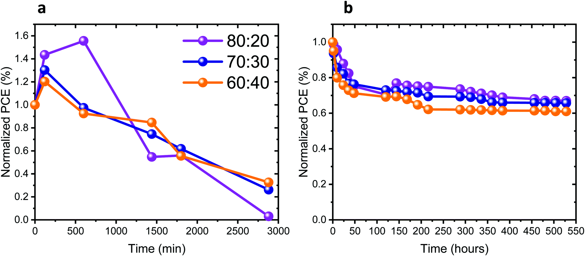 | ||
| Fig. 7 (a) Stability under 1 sun illumination of complete solar cells with different ratios of Pb:Sn as discussed in this work. (b) Stability of the cells stored under an inert atmosphere and measured in the open air with encapsulation. | ||
3. Conclusion
In this work, CsSnyPb1−yBrxI3−x all inorganic perovskites were synthesized at various ratios of Pb:Sn. Stability and photostability measurements show that Sn stabilizes the CsPbI3 black PV active phase. The Cs cation shrinks the cubic structure and as a result slows down the oxidation of Sn. The Hall effect measurement shows an increase in the mobility and in the charge carrier density with the addition of Sn to the structure. UPS reveals an upward shift of the VBM and a small increase in the CBM, which provide a decrease in the band gap with the increase of the Sn amount in the structure. Finally, these compounds were introduced into mesoporous material based perovskite solar cells, achieving 12.7% power conversion efficiency. As the Sn amount increases, the PV performance decreases due to phase mixing of the active cubic phase and the nonactive orthorhombic phase supported by DFT calculations.
4. Experimental section
Film fabrication
Microscope glass was cleaned with ethanol and acetone. Oxygen plasma treatment (80% power, Diener) was performed before deposition of the perovskite solution.Device fabrication
SnO2/(FTO) conductive glass (10 Ohm cm−1, Pilkington) was etched by the reaction of zinc powder with HCl (37% Sigma) on top of the glass. After etching, the glass was cleaned in a sonication bath for 15 minutes followed by oxygen plasma treatment (80% power, Diener). The compact TiO2 (TiDIP, 75% in isopropanol, Aldrich, diluted 1:5 in isopropanol) layer was deposited on the substrate by spin coating (5000 rpm for 30 seconds), followed by deposition of m-TiO2 nanoparticles (30-NRD, dyesol) (1:6 w/w% in ethanol absolute) by spin-coating (5000 rpm for 30 seconds); then the substrate was annealed at 450 °C for 30 min. TiCl4 was applied on the m-TiO2 film.
For the perovskite deposition, 60 μl of perovskite solution was dropped on the middle of the substrate, followed by a spin-coating process with a five second delay time, ten second spin at 1000 rpm, and 45 second spin at 5000 rpm. 25 seconds before the end of the spin coating, 50 μl of toluene was added dropwise onto the substrate. The cells were annealed at 110 °C for two minutes. Next, the PTAA film was deposited: a PTAA (Ossila)/toluene (15 mg/1 ml) solution with 13.6 ml of Li-bis(trifluoromethanesulfonyl) imide (Li-TFSI)/acetonitrile (28.3 mg/1 ml) and 6.8 ml TBP added was spin-coated at 3000 rpm for 30 seconds and annealed at 75 °C for five minutes. Finally, a 70 nm thick gold electrode was thermally evaporated on the film under a vacuum of ∼10−7 Torr.
Preparation of perovskite solutions
The perovskite solutions were prepared in a nitrogen filled glovebox H2O < 0.1 ppm and O2 < 5.0 ppm. All of the inorganic precursors were purchased from Sigma Aldrich. A CsSnyPb1−yBrxI3−x (different ratios) solution of 0.48 M was prepared by dissolving CsI, PbI2, and SnBr2 in a mixture of dimethylformamide:dimethyl sulfoxide (DMF/DMSO) (85%:15%). A CsSnI3 solution (0.48 M) was prepared by dissolving CsI, PbI2, and SnI2 in a mixture of dimethylformamide:dimethyl sulfoxide (DMF/DMSO) (85%:15%). The perovskite solutions were prepared 12 hours before the perovskite deposition.
Encapsulation
Encapsulation was done with a Meltonix 1170-60 (Solaronix) and cover glasses (PAUL MARIENFELD) in a nitrogen environment.Absorbance measurements
Absorbance measurements were performed using a Jasco V-670 spectrophotometer.X-ray diffraction (XRD)
X-ray powder diffraction measurements were performed in grazing incidence X-ray diffraction (GIXRD) mode on a D-8 Advance diffractometer (Bruker AXS, Karlsruhe, Germany) with a goniometer radius of 217.5 mm, a secondary graphite monochromator, 2° Soller slits and a 0.2 mm receiving slit. XRD patterns within the range 2° to 60° (2θ) were taken at 273 K using CuKα radiation (λ 1.5418 Å) with the following measurement conditions: a tube voltage of 40 kV, a tube current of 40 mA, step-scan mode with a step size of 0.02° (2θ) and a counting time of 1 s−3 s per step. The value of the grazing incidence angle was 2.5°.Ultra high resolution scanning electron microscopy (UHR-SEM)
The images were attained by using a Sirion UHR SEM of FEI (Field Emission Instruments). The measurement conditions were 5 kV, the spot size was 3.0, and the detector was TLS.Hall effect
Hall effect measurements were made using a Lake Shore dc Hall effect system model 8404. A magnetic field of 1.7 T, and a current of 100 nA were used in the measurement. The samples were illuminated with 0.25 sun of a white LED source. Each measurement was conducted 20 times, and the average results and the standard deviations were used in the calculation of the final values. Also, in these measurements we used the high resistivity option in order to achieve reliable results.Ultraviolet photoelectron spectroscopy (UPS)
UPS measurements were performed in an ultrahigh vacuum at room temperature. He I photons (21.22 eV) generated by a discharge lamp were used to probe the work function and valence band edges.Photovoltaic characterization
Photovoltaic measurements were performed using a Newport system, composed of an Oriel I–V test station using an Oriel Sol3A simulator. The solar simulator is class AAA for spectral performance, uniformity of irradiance, and temporal stability. The solar simulator is equipped with a 450 W xenon lamp. The output power is adjusted to match AM1. The spectrally matched classic cations are IEC60904-9 2007, JIC C 8912, and ASTM E927-05.DFT calculations
The density functional theory (DFT) calculations of the band gaps were performed with the Quantum ESPRESSO code,65 using a plane-wave basis and norm-conserving pseudopotentials for the atomic cores. The Perdew–Burke–Ernzerhof parametrization of the exchange–correlation functional was chosen. Spin–orbit coupling was not included, because its effect on the bandgaps in perovskites is balanced by neglecting the self-interaction correction (see Table 5 in ref. 66).The doped crystals were calculated using 40-atom supercells, which were eight times larger than the elementary cubic cell (four atoms) and two times larger than the elementary orthorhombic cell (20 atoms). A uniform k-mesh of 4 × 4 × 4 points in the Brillouin zone was used for the supercells, and a two times larger grid for the pure compounds.
Conflicts of interest
There are no conflicts to declare.Acknowledgements
This research was supported by the Israel Science Foundation grant No. 937/18 and 2552/17. Calculations were performed using the PL-GRID infrastructure (Prometheus computer and supported by the National Science Centre in Poland (grant 2019/33/B/ST8/02105)). Work in Princeton was supported by the US-Israel Binational Science Foundation (BSF Grant No. 2018349).References
- C. R. Kagan, D. B. Mitzi and C. D. Dimitrakopoulos, Science, 1999, 286, 945–947 CrossRef CAS PubMed.
- Y. Fu, H. Zhu, J. Chen, M. P. Hautzinger, X. Y. Zhu and S. Jin, Nat. Rev. Mater., 2019, 4, 169–188 CrossRef CAS.
- J. Shamsi, A. S. Urban, M. Imran, L. De Trizio and L. Manna, Chem. Rev., 2019, 119, 3296–3348 CrossRef CAS PubMed.
- W. J. Nimens, S. J. Lefave, L. Flannery, J. Ogle, D.-M. Smilgies, M. T. Kieber-Emmons and L. Whittaker-Brooks, Angew. Chem., Int. Ed., 2019, 58, 13912–13921 CrossRef CAS PubMed.
- G. E. Eperon, S. N. Habisreutinger, T. Leijtens, B. J. Bruijnaers, J. J. van Franeker, D. W. deQuilettes, S. Pathak, R. J. Sutton, G. Grancini, D. S. Ginger, R. A. J. Janssen, A. Petrozza and H. J. Snaith, ACS Nano, 2015, 9, 9380–9393 CrossRef CAS PubMed.
- Q. Wang, B. Chen, Y. Liu, Y. Deng, Y. Bai, Q. Dong and J. Huang, Energy Environ. Sci., 2017, 10, 516–522 RSC.
- X. Li, M. Ibrahim Dar, C. Yi, J. Luo, M. Tschumi, S. M. Zakeeruddin, M. K. Nazeeruddin, H. Han and M. Grätzel, Nat. Chem., 2015, 7, 703–711 CrossRef CAS PubMed.
- G. Abdelmageed, L. Jewell, K. Hellier, L. Seymour, B. Luo, F. Bridges, J. Z. Zhang and S. Carter, Appl. Phys. Lett., 2016, 109, 233905 CrossRef.
- N. Chander, A. F. Khan, P. S. Chandrasekhar, E. Thouti, S. K. Swami, V. Dutta and V. K. Komarala, Appl. Phys. Lett., 2014, 105, 033904 CrossRef.
- F. Yang, D. Hirotani, G. Kapil, M. A. Kamarudin, C. H. Ng, Y. Zhang, Q. Shen and S. Hayase, Angew. Chem., 2018, 130, 12927–12931 CrossRef.
- S. Xiang, W. Li, Y. Wei, J. Liu, H. Liu, L. Zhu and H. Chen, Nanoscale, 2018, 10, 9996–10004 RSC.
- Y. Liang, L. Guan, X. Xu, S. Han, J. Guo, J. Wang, X. Chen, Z. Zhang and X. Li, J. Phys. Chem. C, 2020, 124, 6028–6037 CrossRef CAS.
- A. Swarnkar, W. J. Mir and A. Nag, ACS Energy Lett., 2018, 3, 286–289 CrossRef CAS.
- Y. Wu, F. Xie, H. Chen, X. Yang, H. Su, M. Cai, Z. Zhou, T. Noda and L. Han, Adv. Mater., 2017, 29, 1701073 CrossRef.
- K. Pinsuwan, C. Boonthum, T. Supasai, S. Sahasithiwat, P. Kumnorkaew and P. Kanjanaboos, J. Mater. Sci., 2020, 55, 3484–3494 CrossRef CAS.
- E. V. Péan, C. S. De Castro and M. L. Davies, Mater. Lett., 2019, 243, 191–194 CrossRef.
- D. A. Gidlow, Occup. Med., 2004, 54, 76–81 CrossRef CAS.
- G. Flora, D. Gupta and A. Tiwari, Interdiscip. Toxicol., 2012, 5, 47–58 CAS.
- R. A. Goyer, Environ. Health Perspect., 1993, 100, 177–187 CrossRef CAS PubMed.
- F. Li and M. Liu, J. Mater. Chem. A, 2017, 5, 15447–15459 RSC.
- G. E. Eperon, G. M. Paternò, R. J. Sutton, A. Zampetti, A. A. Haghighirad, F. Cacialli and H. J. Snaith, J. Mater. Chem. A, 2015, 3, 19688–19695 RSC.
- J. K. Nam, S. U. Chai, W. Cha, Y. J. Choi, W. Kim, M. S. Jung, J. Kwon, D. Kim and J. H. Park, Nano Lett., 2017, 17, 2028–2033 CrossRef CAS PubMed.
- M. Saliba, T. Matsui, J.-Y. Seo, K. Domanski, J.-P. Correa-Baena, M. K. Nazeeruddin, S. M. Zakeeruddin, W. Tress, A. Abate, A. Hagfeldt and M. Grätzel, Energy Environ. Sci., 2016, 9, 1989–1997 RSC.
- C. Liu, W. Li, H. Li, H. Wang, C. Zhang, Y. Yang, X. Gao, Q. Xue, H.-L. Yip, J. Fan, R. E. I. Schropp and Y. Mai, Adv. Energy Mater., 2019, 9, 1803572 CrossRef.
- W. Xiang, Z. Wang, D. J. Kubicki, W. Tress, J. Luo, D. Prochowicz, S. Akin, L. Emsley, J. Zhou, G. Dietler, M. Grätzel and A. Hagfeldt, Joule, 2019, 3, 205–214 CrossRef CAS.
- T. Zhang, M. I. Dar, G. Li, F. Xu, N. Guo, M. Grätzel and Y. Zhao, Sci. Adv., 2017, 3, e1700841 CrossRef PubMed.
- A. Marronnier, G. Roma, S. Boyer-Richard, L. Pedesseau, J.-M. Jancu, Y. Bonnassieux, C. Katan, C. C. Stoumpos, M. G. Kanatzidis and J. Even, ACS Nano, 2018, 12, 3477–3486 CrossRef CAS PubMed.
- A. Shpatz Dayan, B.-E. Cohen, S. Aharon, C. Tenailleau, M. Wierzbowska and L. Etgar, Chem. Mater., 2018, 30, 8017–8024 CrossRef CAS.
- F. O. Saouma, C. C. Stoumpos, J. Wong, M. G. Kanatzidis and J. I. Jang, Nat. Commun., 2017, 8, 742 CrossRef CAS PubMed.
- A. K. Jena, A. Kulkarni, Y. Sanehira, M. Ikegami and T. Miyasaka, Chem. Mater., 2018, 30, 6668–6674 CrossRef CAS.
- H. Zhao, J. Xu, S. Zhou, Z. Li, B. Zhang, X. Xia, X. Liu, S. Dai and J. Yao, Adv. Funct. Mater., 2019, 29, 1808986 CrossRef.
- T. Fujihara, S. Terakawa, T. Matsushima, C. Qin, M. Yahiro and C. Adachi, J. Mater. Chem. C, 2017, 5, 1121–1127 RSC.
- W. Ke, C. C. Stoumpos, I. Spanopoulos, L. Mao, M. Chen, M. R. Wasielewski and M. G. Kanatzidis, J. Am. Chem. Soc., 2017, 139, 14800–14806 CrossRef CAS PubMed.
- G. C. Papavassiliou and I. B. Koutselas, Synth. Met., 1995, 71, 1713–1714 CrossRef CAS.
- C. C. Stoumpos, C. D. Malliakas and M. G. Kanatzidis, Inorg. Chem., 2013, 52, 9019–9038 CrossRef CAS PubMed.
- E. J. W. Whittaker and R. Muntus, Geochim. Cosmochim. Acta, 1970, 34, 945–956 CrossRef CAS.
- G. Kieslich, S. Sun and A. K. Cheetham, Chem. Sci., 2014, 5, 4712–4715 RSC.
- Z. Li, M. Yang, J. S. Park, S. H. Wei, J. J. Berry and K. Zhu, Chem. Mater., 2016, 28, 284–292 CrossRef CAS.
- M. Deepa, M. Salado, L. Calio, S. Kazim, S. M. Shivaprasad and S. Ahmad, Phys. Chem. Chem. Phys., 2017, 19, 4069–4077 RSC.
- D. Sabba, H. K. Mulmudi, R. R. Prabhakar, T. Krishnamoorthy, T. Baikie, P. P. Boix, S. Mhaisalkar and N. Mathews, J. Phys. Chem. C, 2015, 119, 1763–1767 CrossRef CAS.
- I. Chung, B. Lee, J. He, R. P. H. Chang and M. G. Kanatzidis, Nature, 2012, 485, 486–489 CrossRef CAS PubMed.
- N. Wang, Y. Zhou, M.-G. Ju, H. F. Garces, T. Ding, S. Pang, X. C. Zeng, N. P. Padture and X. W. Sun, Adv. Energy Mater., 2016, 6, 1601130 CrossRef.
- H. Xu, J. Duan, Y. Zhao, Z. Jiao, B. He and Q. Tang, J. Power Sources, 2018, 399, 76–82 CrossRef CAS.
- B. Li, R. Long, Y. Xia and Q. Mi, Angew. Chem., Int. Ed., 2018, 57, 13154–13158 CrossRef CAS PubMed.
- F. Reyes-Pérez, J. J. Gallardo, T. Aguilar, R. Alcántara, C. Fernández-Lorenzo and J. Navas, ChemistrySelect, 2018, 3, 10226–10235 CrossRef.
- S. Liu, L. Yuan, Y. Zhao, Y. Chen, W. Xiang and X. Liang, J. Alloys Compd., 2019, 806, 1022–1028 CrossRef CAS.
- J. Liang, P. Zhao, C. Wang, Y. Wang, Y. Hu, G. Zhu, L. Ma, J. Liu and Z. Jin, J. Am. Chem. Soc., 2017, 139, 14009–14012 CrossRef CAS PubMed.
- N. Li, Z. Zhu, J. Li, A. K.-Y. Jen and L. Wang, Adv. Energy Mater., 2018, 8, 1800525 CrossRef.
- J. L. Knutson, J. D. Martin and D. B. Mitzi, Inorg. Chem., 2005, 44, 4699–4705 CrossRef CAS PubMed.
- A. Goyal, S. McKechnie, D. Pashov, W. Tumas, M. Van Schilfgaarde and V. Stevanović, Chem. Mater., 2018, 30, 3920–3928 CrossRef CAS.
- T. Leijtens, R. Prasanna, A. Gold-Parker, M. F. Toney and M. D. McGehee, ACS Energy Lett., 2017, 2, 2159–2165 CrossRef CAS.
- R. K. Misra, L. Ciammaruchi, S. Aharon, D. Mogilyansky, L. Etgar, I. Visoly-Fisher and E. A. Katz, ChemSusChem, 2016, 9, 2572–2577 CrossRef CAS.
- M. Zhang, M. Ye, W. Wang, C. Ma, S. Wang, Q. Liu, T. Lian, J. Huang and Z. Lin, Adv. Mater., 2020, 32, 2000999 CrossRef CAS.
- X. D. Zhu, Y. Xie and Y. T. Liu, J. Mater. Chem. A, 2018, 6, 21255–21260 RSC.
- Y. Takahashi, H. Hasegawa, Y. Takahashi and T. Inabe, J. Solid State Chem., 2013, 205, 39–43 CrossRef CAS.
- C. Wehrenfennig, G. E. Eperon, M. B. Johnston, H. J. Snaith and L. M. Herz, Adv. Mater., 2014, 26, 1584–1589 CrossRef CAS PubMed.
- G. Xing, N. Mathews, S. Sun, S. S. Lim, Y. M. Lam, M. Gratzel, S. Mhaisalkar and T. C. Sum, Science, 2013, 342, 344–347 CrossRef CAS PubMed.
- A. Miyata, A. Mitioglu, P. Plochocka, O. Portugall, J. T. W. Wang, S. D. Stranks, H. J. Snaith and R. J. Nicholas, Nat. Phys., 2015, 11, 582–587 Search PubMed.
- L. Ji, X. Zhang, T. Zhang, Y. Wang, F. Wang, Z. Zhong, Z. D. Chen, Z. Xiao, L. Chen and S. Li, J. Mater. Chem. A, 2019, 7, 9154–9162 RSC.
- F. Hao, C. C. Stoumpos, D. H. Cao, R. P. H. Chang and M. G. Kanatzidis, Nat. Photonics, 2014, 8, 489–494 CrossRef CAS.
- V. K. Ravi, G. B. Markad and A. Nag, ACS Energy Lett., 2016, 1, 665–671 CrossRef CAS.
- C. Liu, M. Hu, X. Zhou, J. Wu, L. Zhang, W. Kong, X. Li, X. Zhao, S. Dai, B. Xu and C. Cheng, NPG Asia Mater., 2018, 10, 552–561 CrossRef CAS.
- Y. Hu, F. Bai, X. Liu, Q. Ji, X. Miao, T. Qiu and S. Zhang, ACS Energy Lett., 2017, 2, 2219–2227 CrossRef CAS.
- F. Haque, M. Wright, M. A. Mahmud, H. Yi, D. Wang, L. Duan, C. Xu, M. B. Upama and A. Uddin, ACS Omega, 2018, 3, 11937–11944 CrossRef CAS PubMed.
- P. Giannozzi, S. Baroni, N. Bonini, M. Calandra, R. Car, C. Cavazzoni, D. Ceresoli, G. L. Chiarotti, M. Cococcioni, I. Dabo, A. Dal Corso, S. De Gironcoli, S. Fabris, G. Fratesi, R. Gebauer, U. Gerstmann, C. Gougoussis, A. Kokalj, M. Lazzeri, L. Martin-Samos, N. Marzari, F. Mauri, R. Mazzarello, S. Paolini, A. Pasquarello, L. Paulatto, C. Sbraccia, S. Scandolo, G. Sclauzero, A. P. Seitsonen, A. Smogunov, P. Umari and R. M. Wentzcovitch, J. Phys.: Condens. Matter, 2009, 21, 395502 CrossRef PubMed.
- M. Wierzbowska, J. J. Meléndez and D. Varsano, Comput. Mater. Sci., 2018, 142, 361–371 CrossRef CAS.
Footnote |
| † Electronic supplementary information (ESI) available. See DOI: 10.1039/d0ma00452a |
| This journal is © The Royal Society of Chemistry 2020 |