
Research on the influence of ultraviolet radiation on OLEDs and the luminance attenuation model of light aging
Lulu
Zhou
ace,
Zhanhan
Hu
d,
Wei
Shi
 *abe,
Yixiao
Zhang
ace,
Yangyang
Zhu
ae,
Yi
Liao
ae,
Yachen
Xu
ae,
Jialu
Gu
ae,
Weixia
Lan
a and
Bin
Wei
*abe
*abe,
Yixiao
Zhang
ace,
Yangyang
Zhu
ae,
Yi
Liao
ae,
Yachen
Xu
ae,
Jialu
Gu
ae,
Weixia
Lan
a and
Bin
Wei
*abe
aSchool of Mechatronic Engineering and Automation, Shanghai University, Shanghai, 200444, P. R. China. E-mail: shiwei@shu.edu.cn; bwei@shu.edu.cn
bShanghai Engineering Research Center for Integrated Circuits and Advanced Display Materials, Shanghai University, Shanghai 200072, P. R. China
cMicroelectronic R&D Center, School of Mechatronic Engineering and Automation, Shanghai University, Shanghai 200072, P. R. China
dNorth China Institute of Aerospace Engineering, Langfang, Hebei Province, P. R. China
eKey Laboratory of Advanced Display and System Applications, Ministry of Education, Shanghai University, Shanghai, 200072, P. R. China
First published on 15th April 2025
Abstract
We investigated the degradation performance of organic light-emitting diodes (OLEDs) under different ultraviolet (UV) irradiation intensities and demonstrated that the stretched exponential decay (SED) model, applicable in electrical aging, is also suitable for describing the luminance–time curves in photoaging. In this way, OLED lifetime acquired at low UV illumination could be fitted with that obtained at high illumination. We also demonstrated how UV radiation affects the interface at the ITO/hole transport layer, which led to its degradation. This was elucidated through changes in the mobility of single-carrier devices and XPS characterization of the films before and after UV irradiation. These findings reveal the external behavior and internal mechanism of OLEDs in light aging, providing a reliable research direction for enhancing the stability of organic electronic devices.
1. Introduction
Organic light-emitting diodes (OLEDs), known for their uniform illumination, low power consumption, long lifespan, light weight, and flexible design, are widely used in various fields such as lighting sources, wearable devices, screen displays, automotive equipment, and AR/VR devices.1–6 However, the attenuation mechanism of OLEDs is a noteworthy issue to promote its commercial application. The aging of OLEDs commonly stems from the internal factors, such as excitons, charge carriers, and material changes, and the external factors, like light, water and oxygen, temperature, and fabrication parameters (pressure, evaporation rate, impurities, etc.).7Outdoor OLEDs, especially car taillights, are vulnerable to harsh environmental conditions, such as prolonged exposure to high temperature or ultraviolet (UV) radiation, which can lead to poor performance, shorter life, and even damage (complete breakdown).8–11 In outdoor environments, UV light (300–400 nm) possesses significantly higher photon energy than visible light, enabling direct cleavage of critical chemical bonds in OLED materials and triggering irreversible degradation. Not only OLEDs, organic solar cells (OSCs), organic transistors and other organic electronic devices are prone to efficiency degradation, functional failure, and shortened service life under intense UV radiation due to the structure and properties of organic materials.12–14 Therefore, it is of distinct significance to study the change and attenuation model of OLEDs under UV irradiation.
J. Askola et al. studied commercial OLED panels and found that for the same panel, UV exposure increased brightness attenuation by up to 8 times compared to natural aging.15 R. Seifert et al. have demonstrated that the exponential relationship between the half-life and current density (J) of OLEDs, which is well-known under electrical aging, is also applicable under UV aging.16 S.-K. Kwon et al. fabricated a Yb:LiF cathode unit in red phosphorescent top-emitting OLEDs to resist the adverse effects of ultraviolet light, such as loss of brightness and lifespan, as well as pixel shrinkage, on the device.17 However, the aforementioned studies lack a systematic demonstration of UV-induced damage at the device level, and research on UV-induced luminance degradation models remains less prevalent compared to electrical aging models.
Here, we fabricated a high-performance red OLED and conducted optoelectronic performance testing. After encapsulating the OLED with a glass cover plate, T90 lifetime (time to 90% of the initial luminance) tests were conducted under UV irradiation intensities of 60, 90, and 120 mW cm−2. The changes in electrical and optical properties under a fixed J were observed and analyzed. By fitting the luminance (L) decay curve and constructing a model, it was found that this light aging model is similar to the electrical aging model, both following an exponential decay pattern. Additionally, single-carrier devices were fabricated to illustrate the changes in carrier mobility before and after irradiation, and XPS testing was employed to characterize the change in the ITO/hole transport layer (HTL) interface.
2. Experimental
The luminescent host material 4,4′-bis(N-carbazolyl)-1,1′-biphenyl (CBP), luminescent guest material bis[1-(phenyl)isoquinoline]iridium(III)(acetylacetonate) (Ir(piq)2acac), electronic transport material 1,3,5-tris(2-N-phenylbenzimidazolyl)benzene (TPBi), electron injection material Liq, HTL 4,4′,4′′-tris(carbazol-9-yl)triphenylamine (TCTA) and N,N′-bis(naphthalen-1-yl)-N,N′-bis(phenyl)-benzidine (NPB) were purchased from Lumtec Company in Taiwan, and the purity was above 99.5%. MoO3 powder was purchased from Sinopod Group with a purity of over 95%. ITO (15 Ω sq−1, 150 nm)-coated glass substrates were ultrasonically cleaned using detergent, de-ionized water, acetone, isopropanol, and treated with UV-ozone for 20 min. Keep the surface of the glass cover-plate clean before encapsulating. Apply liquid desiccant to the grooves of the glass cover and UV adhesive (UV681, Permabond) to the edges. After coating, place it on the OLED (top side up) and immediately cure under UV light for 2–3 s to complete the encapsulation. The light aging lifetime test of the encapsulated OLED is conducted in air, with UV light irradiated on the anode (bottom) of the OLED. During irradiation, the OLED remains in an open-circuit state. When performing photoelectric performance tests on the OLED, light is emitted from the bottom ITO side, thus it is not affected by the glass cover-plate.The structure of device D1 is ITO/NPB:10%MoO3 (40 nm)/TCTA (10 nm)/CBP:6% Ir(piq)2acac (20 nm)/TPBi (40 nm)/Liq (1 nm)/Al (100 nm). The structure of single-hole device H1 is ITO/NPB:10% MoO3 (40 nm)/Al (100 nm) and irradiated under 120 mW cm−2 UV for 12 h. The structure of single-hole device H2 is ITO/NPB:10% MoO3 (40 nm) and irradiated under 120 mW cm−2 UV for 12 h/Al (100 nm). The structure of single-electron device E1 is ITO/Liq (1 nm)/TPBi (40 nm)/Liq (1 nm)/Al (100 nm) and irradiated under 120 mW cm−2 UV for 12 h. The structure of single-electron device E2 is ITO/Liq (1 nm)/TPBi (40 nm)/Liq (1 nm)/Al (100 nm) and irradiated under 120 mW cm−2 UV for 12 h before Al evaporation. For devices H1 and E1, the evaporation was conducted first and then UV irradiated. For devices H2 and E2, the UV irradiation was conducted first and then evaporated.
Fig. 1 shows the device structure diagram, energy level diagram, and encapsulated OLED diagram of device D1. Both the films and the devices were prepared in vacuum evaporation equipment with pressure less than 5 × 10⁻⁵ mbar. The evaporation rate of the single-layer organic film was 0.6–1.2 Å s−1, and the evaporation rate of the metal Al electrode was above 5 Å s−1. The J–Voltage–L (J–V–L) characteristics of the device were measured by using a Keithley 2400 source meter and a PR-650 spectrometer. The current–V (I–V) characteristics of the single-carrier device were measured by using a Keithley 2400 source meter and XPS/UPS tests were performed on a Nexsa spectrometer. The luminescence images of the device were observed under an optical microscope (Leika DM4000M). The UV light source is a point light source with a wavelength of 365 nm, a power of 10 W and a spot diameter of 10 mm. The UV irradiation intensities in the experiment were set to 60, 90, and 120 mW cm−2.
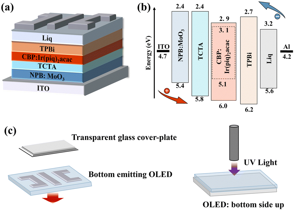 | ||
| Fig. 1 (a) Device structure. (b) Energy level alignment. (c) Schematic diagram of glass lid encapsulation of the OLED and UV test. | ||
3. Results and discussion
3.1 UV damage to the device
Fig. 2(a) and (b) show the J–V–L and L–current efficiency–power efficiency (L–CE–PE) characteristics of the red-light OLED. The device has a turn-on voltage of 3.1 V, a maximum L (Lmax) of 23298 cd m−2, and achieves a maximum external quantum efficiency (EQEmax) of 17.75% at 3.5 V, with a CEmax of 13.8 cd A−1. The overall optoelectronic performance and efficiency are relatively good, which lays a solid foundation for the subsequent photoaging experiments. | ||
| Fig. 2 (a) J–V–L and (b) L–CE–PE of pristine device D1. (c) J–V–L, (d) L–CE–PE, and (e) EL spectra of device D1 at initial state, 5 h, 20 h, and 45 h under 120 mW cm−2 UV irradiance. | ||
Fig. 2(c)–(e) present the study of the luminescence performance of device D1 at 120 mw cm−2 UV irradiation of 5, 20, and 45 h, which are close to T90, T70, and T50 of the device lifetime, respectively. Fig. 2(c) shows that as the irradiation time increases, both J and L exhibit a downward trend. Similarly, the declining trends in CE and PE can also be observed in Fig. 2(d). In Fig. 2(e), for the electroluminescence (EL) spectra at different irradiation durations, the position of the main emission peak remains basically unchanged. However, a small peak appears at 432/436 nm, showing an increasing trend with prolonged UV irradiation time. Given the photoluminescence (PL) peaks of TCTA (HTL) at ∼404.5 nm and TPBi (electron transport layer) at ∼379 nm,18 along with the large energy barrier between them, we attribute this to the formation of the TCTA/TPBi exciplex19 (PL peak at 437 nm) under high-intensity UV irradiation. As the irradiation time increased, more exciplex formed, leading to the enhancement of the emission peak. In summary, as the UV irradiation time increases, OLEDs experience progressively more severe damage. However, this damage is not reflected in the main emission peak of the EL spectrum but primarily manifests in performance aspects such as the turn-on voltage and luminescence efficiency.
Next, we investigated the changes in L and V over time (T) for OLEDs under three UV irradiation intensities (60, 90, and 120 mW cm−2) at a fixed J of 10 mA cm−2. Fig. 3(a) illustrates the voltage increase compared to the initial voltage over time (V–T). Here, the impact of 120 mW cm−2 UV irradiance was particularly significant, with the V changed exceeding 20% compared to the initial V after just 13 h. In Fig. 3(b), the corresponding T90 values of device D1 at the irradiation intensities of 120, 90 and 60 mW cm−2 were 5, 18 and 78 h, respectively. And regardless of the intensity of illumination, at the beginning of ultraviolet irradiation, there was a phenomenon of enhancement in brightness. Then the variation trend of brightness in the irradiation process basically conformed to the law of exponential functions. Fig. 3(c) reveals that the variations in EQE closely mirror those in luminance. Despite the linear rise in the UV irradiation intensity, the deterioration in device performance became more pronounced at higher irradiance levels. We also conducted microscopy imaging on OLEDs irradiated at 90 mW cm−2 and 120 mW cm−2 for 50 h. As shown in Fig. 3(d) and (e), the latter exhibits significantly more black spots than the former, with a more widespread distribution.
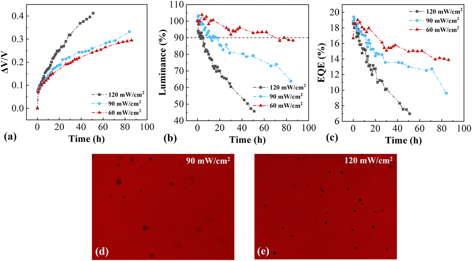 | ||
| Fig. 3 (a) V–T, (b) L–T, and (c) EQE–T characteristics of device D1 at UV irradiances of 60, 90, and 120 mW cm−2 at 10 mA cm−2. Microscopic images of device D1 after 50 h of UV irradiances at (d) 90 mW cm−2 and (e) 120 mW cm−2. | ||
3.2 Luminance attenuation model
The luminance decay models of OLEDs under UV irradiation intensities of 60, 90, and 120 mW cm−2 were simulated and analyzed. The luminance decay of OLEDs is typically caused by multiple parallel degradation pathways (such as interface defect formation and exciton quenching), and the stretched exponential decay (SED) model can more accurately describe this complex decay behavior with non-single timescale characteristics. The SED model is applicable not only to electrical aging but also to thermal aging analysis.11 In photoaging experiments, because OLED degradation curves exhibit similar characteristics, the SED model was also employed for data fitting, expressed as:20 | (1) |
Similarly, we investigate the relationship between the half-lifetime fitted with the SED model and the UV illuminance. The relationship between the half-lifetime and the initial brightness in electric aging complies with:
| t0.5 × L0n = C | (2) |
| t0.5 × IUVn = C | (3) |
As illustrated in the log-double diagram of Fig. 4(b), there is a linear relationship between the half-lifetime and UV illumination. The significance of Fig. 4 lies in two main aspects: first, the luminance attenuation model under electrical aging is also applicable to UV aging; second, the accelerated aging tests of OLEDs can be conducted with high UV illumination, offering a dependable method to estimate their lifespan under low irradiance.
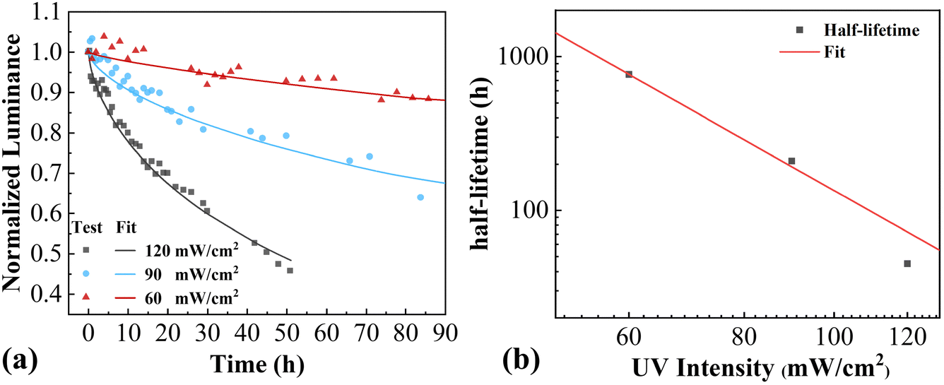 | ||
| Fig. 4 (a) SED model of L–T characteristics under UV irradiances of 60, 90, and 120 mW cm−2. (b) The relationship between UV intensity and half-lifetime of device D1. | ||
3.3 Mechanism of UV damage to the device
To study the UV damage mechanisms and whether organic materials or interfaces are affected, we fabricated single-carrier devices and measured carrier mobility changes before and after UV exposure at 120 mW cm−2 under vacuum for 12 h. Two groups of single-electron devices were prepared, and the difference was that one was UV-irradiated after Al deposition (device E1, Fig. 5(a)), while the other one was UV-irradiated before Al deposition (device E2, Fig. 5(b)). The control group was taken from different luminescent spots on the same sample shielded with black tape to avoid UV effects. It can be observed that for single-electron devices, the carrier mobility showed little difference and even slightly increased compared to the control group. This indicated that the damage caused by UV light was not located at the interface of the organic material/metal cathode. | ||
| Fig. 5 I–V curves of (a) device E1, (b) device E2, (c) device H1, and (d) device H2. | ||
Then we observed the single-hole devices. Fig. 5(c) (device H1) reveals that UV irradiation significantly enhanced hole transport. This should be attributed to the increased work function of the ITO surface,21,22 which reduced the hole transport barrier and facilitated hole injection. As shown in Fig. 6(a), the work function of UV-treated ITO rises from 4.7 eV to 5.3 eV,22 and the hole injection barrier decreases from 0.7 eV to 0.1 eV, greatly improving hole transport. However, as shown in Fig. 5(d), the device irradiated before deposition (device H2) exhibited a significant decrease in hole mobility. We believe that this phenomenon may be related to the introduction of oxygen during the photoaging process, as illustrated in Fig. 6(b). Research indicates that UV irradiation can induce photo-oxidation reactions of organic semiconductor materials. For instance, Choi et al. discovered that under short-wavelength, high-energy (254 nm) UV light exposure, pentacene reacts with the SiO2 substrate, leading to the formation of crystalline defects.23 Especially under insufficient vacuum conditions, residual oxygen can accelerate this aging process and trigger more complex subsequent reactions.24 For device H2 (Fig. 5(d)), such photo-oxidative damage was difficult to repair even after subsequent Al electrode deposition, resulting in a loss of hole transport performance. This finding is consistent with the results reported in the literature that photoaging leads to a decrease in the carrier mobility of organic semiconductor materials.25,26
 | ||
| Fig. 6 Schematics of (a) reduced hole injection barrier in device H1 and (b) device H2. (c) O 1s electron binding energy spectra of ITO/NPB films before and after irradiation. | ||
Comparing Fig. 5(a) and (c), it is revealed that UV irradiation to device H1 enhances carrier mobility, with holes improving more than electrons. Given that the hole mobility in OLEDs is much higher than electron mobility,27,28 this further aggravates the imbalance in carrier recombination, thereby reducing the luminous efficiency of the OLEDs. In addition, as single-electron devices showing UV light hardly affect the organic/cathode interface, the damage of device H2 may originate from the organic material itself or the ITO/HTL interface. This could also be inferred from the results that PL characteristics of the organic compounds remain basically unchanged after UV irradiation.25,29 In contrast, device H2 (Fig. 5(d)) experienced unavoidable oxygen exposure during photoaging after ITO/HTL interface preparation, resulting in UV-induced photo-oxidation and a significant drop in hole mobility. To conclude, we infer that the main area impacted by UV light inside the device is the ITO/HTL interface layer.
After studying the changes in carrier mobility of single-carrier devices after UV irradiation, we aimed to know whether the photoaging reaction at the ITO/HTL interface is fundamentally chemical. To this end, we conducted XPS characterization on ITO/NPB (40 nm) films before and after UV-irradiation. To avoid additional effects from atmospheric oxygen, the photo-aging experiment was also carried out under vacuum conditions. One group was kept in the dark for 72 h, while the other group was exposed to UV light for 72 h, irradiated from the ITO side. Fig. 6(c) shows the O 1s electron binding energy spectrum of the ITO/NPB sample. After irradiation, the peak shifted from 532.3 nm to 531.3 nm with reduced intensity, which should correspond to the chemical bond between oxygen in ITO and the aryl groups of NPB.30 Meanwhile the intensity drop suggests that UV light disrupted the hole injection process. Therefore, we concluded that the impact of UV irradiation on the device during the photo-aging test is chemical in nature, potentially causing a peak shift in the chemical bonds at the interface. This change is externally manifested as deteriorated hole injection in single-hole devices and worsened the luminescence performance of OLEDs.
To investigate the changes in the interfacial work function after UV irradiation, we conducted UPS tests on ITO/NPB (40 nm) films (Fig. 7). We prepared two groups, one maintained under dark conditions and the other under UV irradiation (365 nm, 120 mW cm−2) for 72 h, with both groups strictly isolated from air. After UV treatment, the cut-off energy (Ecut-off) increased from 16.79 to 17.19 eV, while the HOMO level decreased from 4.43 to 4.03 eV (HOMO = hν − Ecut-off). This shift may result from UV-induced oxygen vacancy passivation (as presented in the XPS test), which reduced the free electron concentration on the ITO surface, causing the Fermi level (EF) to shift downward and increasing the work function (Φ = hν − (EF − Ecut-off)). In addition, UV exposure may have altered the orientation of organic molecules on the ITO surface, creating an interfacial dipole layer pointing toward the ITO, thereby enhancing the work function.31
 | ||
| Fig. 7 UPS spectra of ITO/NPB films (a) before irradiation and (b) after irradiation. | ||
From the perspective of carrier injection, the increased work function decreases the energy barrier between the HOMO levels of the organic layer, facilitating hole injection while disrupting the carrier recombination balance. From the perspective of OLED lifetime, excessive hole injection shifts the exciton recombination zone toward the electron transport layer and also induces chemical reactions at the ITO/organic interface, consequently shortening the device lifetime.
4. Conclusion
In summary, we systematically demonstrated the detrimental impact of UV radiation on the optoelectronic performance of OLEDs, with the damage intensifying as the irradiation intensity increases. It has been confirmed that the luminance degradation behavior during photoaging is similar to that during electrical aging, both of which can be described by the SED model, providing a reliable basis for predicting the lifetime of OLEDs under low UV illumination. The results from single-carrier devices and XPS characterization demonstrate that the impact of UV light is observed at the ITO/HTL interface and is attributed to chemical changes. Future efforts could focus on incorporating a suitable interlayer to resist UV-induced damage, enhancing the potential of OLEDs for use in automotive devices, space exploration, and extreme environmental conditions.Data availability
Data are available upon reasonable request.Conflicts of interest
There are no conflicts to declare.Acknowledgements
This work was financially supported by the National Key R&D Program of China (2022YFE0109000), the National Natural Science Foundation of China (62304127), and the Scientific Research of the Education Department of Hebei Province (QN2025375).References
- Y. Huang, E.-L. Hsiang, M.-Y. Deng and S.-T. Wu, Light: Sci. Appl., 2020, 9, 105 CrossRef CAS PubMed.
- R. Pode, Renewable Sustainable Energy Rev., 2020, 133, 110043 CrossRef.
- Y. J. Song, J.-W. Kim, H.-E. Cho, Y. H. Son, M. H. Lee, J. Lee, K. C. Choi and S.-M. Lee, ACS Nano, 2020, 14, 1133 CrossRef CAS PubMed.
- W.-J. Joo, J. Kyoung, M. Esfandyarpour, S.-H. Lee, H. Koo, S. Song, Y.-N. Kwon, S. H. Song, J. C. Bae, A. Jo, M.-J. Kwon, S. H. Han, S.-H. Kim, S. Hwang and M. L. Brongersma, Science, 2020, 370, 459 CrossRef CAS PubMed.
- K. Margariti and T. Kamalakis, Opt. Eng., 2021, 60, 046106 CAS.
- C.-M. Kang and H. Lee, J. Inform. Display, 2022, 23, 19 CrossRef.
- S. Scholz, D. Kondakov, B. Lussem and K. Leo, Chem. Rev., 2015, 115, 8449 CrossRef CAS PubMed.
- H. Colditz, R. Kurt and M. Büchel, Appl. Phys. Lett., 2005, 87, 253505 CrossRef.
- K.-C. Lin, W.-K. Lee, B.-K. Wang, Y.-H. Lin, H.-H. Chen, Y.-H. Song, Y.-H. Huang, L.-W. Shih and C.-C. Wu, Opt. Express, 2021, 29, 7654 CrossRef PubMed.
- M. Azrain, M. Mansor, G. Omar, S. Fadzullah, S. Esa, L. Lim, D. Sivakumar and M. Nordin, Synth. Met., 2019, 247, 191 CrossRef CAS.
- A. Al Haddad, A. Picot, L. Canale, P. Dupuis, G. Zissis and P. Maussion, IEEE Trans. Ind. Appl., 2023, 59, 676 CAS.
- J. B. Patel, P. Tiwana, N. Seidler, G. E. Morse, O. R. Lozman, M. B. Johnston and L. M. Herz, ACS Appl. Mater. Interfaces, 2019, 11, 21543 CrossRef CAS PubMed.
- P. Wu, J. Zhang, J. Lu, X. Li, C. Wu, R. Sun, L. Feng, Q. Jiang, B. Lu and X. Pan, IEEE Trans. Electron Devices, 2014, 61, 1431 CAS.
- H. Sun, J. Weickert, H. C. Hesse and L. Schmidt-Mende, Sol. Energy Mater. Sol. Cells, 2011, 95, 3450 CrossRef CAS.
- J. Askola, Y. Calkin, A. Vaskuri, T. Poikonen and E. Ikonen, Light. Res. Technol., 2019, 51, 1263 CrossRef.
- R. Seifert, S. Scholz, B. Lüssem and K. Leo, Appl. Phys. Lett., 2010, 97, 013308 CrossRef.
- S.-K. Kwon, J.-H. Baek, H.-C. Choi, S. K. Kim, R. Lampande, R. Pode and J. H. Kwon, RSC Adv., 2019, 9, 42561 RSC.
- Z. Chen, Z. Lü, J. Pan, Z. Tang and X. Wang, J. Lumin., 2024, 265, 120247 CrossRef CAS.
- Q. Zhang, H. Zhang, X.-W. Zhang, T. Xu and B. Wei, Chin. Phys. B, 2015, 24, 024222 CrossRef.
- C. Féry, B. Racine, D. Vaufrey, H. Doyeux and S. Cinà, Appl. Phys. Lett., 2005, 87, 213502 CrossRef.
- K. Sugiyama, H. Ishii, Y. Ouchi and K. Seki, J. Appl. Phys., 2000, 87, 295 CrossRef CAS.
- Y. Zhou, J. W. Shim, C. Fuentes-Hernandez, A. Sharma, K. A. Knauer, A. J. Giordano, S. R. Marder and B. Kippelen, Phys. Chem. Chem. Phys., 2012, 14, 12014 RSC.
- J.-M. Choi, D. Hwang, J. M. Hwang, J. H. Kim and S. Im, Appl. Phys. Lett., 2007, 90, 113515 CrossRef.
- A. Maliakal, K. Raghavachari, H. Katz, E. Chandross and T. Siegrist, Chem. Mater., 2004, 16, 4980 CrossRef CAS.
- H. Heil, G. Andress, R. Schmechel, H. Von Seggern, J. Steiger, K. Bonrad and R. Sprengard, J. Appl. Phys., 2005, 97, 124501 CrossRef.
- X. Wang, X. Gao, Y. Zhou, Z. Xie, Q. Song, X. Ding and X. Hou, Thin Solid Films, 2008, 516, 2171 CrossRef CAS.
- V. Coropceanu, J. Cornil, D. A. da Silva Filho, Y. Olivier, R. Silbey and J.-L. Bredas, Chem. Rev., 2007, 107, 926 CrossRef CAS PubMed.
- A. P. Kulkarni, C. J. Tonzola, A. Babel and S. A. Jenekhe, Chem. Mater., 2004, 16, 4556 CrossRef CAS.
- R. Schmechel, G. Andress, H. von Seggern, H. Heil, J. Steiger, K. Bonrad and R. Sprengard, J. Appl. Phys., 2005, 97, 124501 CrossRef.
- S. Kumar, G. Bouyssoux and F. Gaillard, Surf. Interface Anal., 1990, 15, 531 CrossRef CAS.
- H. Ishii, K. Sugiyama, E. Ito and K. Seki, Adv. Mater., 1999, 11, 605 CrossRef CAS.
| This journal is © the Owner Societies 2025 |