
Fabrication of fully non-vacuum processed perovskite solar cells using an inorganic CuSCN hole-transporting material and carbon-back contact
Ajay K.
Baranwal
 *,
Hiroyuki
Kanda
,
Naoyuki
Shibayama
and
Seigo
Ito
*
*,
Hiroyuki
Kanda
,
Naoyuki
Shibayama
and
Seigo
Ito
*
University of Hyogo, Department of Materials and Synchrotron Radiation Engineering, Graduate School of Engineering, 2167 Shosha, Himeji, Hyogo 671-2280, Japan. E-mail: ajaybarn@gmail.com; itou@eng.u-hyogo.ac.jp
First published on 23rd October 2018
Abstract
Fully non-vacuum processed perovskite solar cells have been demonstrated using cheap inorganic copper(I) thiocyanate (CuSCN) as an efficient hole transporting layer in conjunction with low temperature processed carbon back electrodes. The CuSCN interlayer attained better energetic matching and assisted the easy release of holes, reducing the observed hysteresis. The fabricated PSC (F-doped SnO2 glass (FTO)/dense TiO2/porous TiO2/CH3NH3PbI3/CuSCN/carbon) was able to realize a power conversion efficiency (PCE) of 12.41%, measured under 100 mW cm−2 illumination with a short circuit current density of 18.90 mA cm−2, an open circuit voltage of 0.95 V and a fill factor of 0.68. An advantageous 68% of the initial PCE was retained for the unencapsulated PSC stored in air in the dark, measured over 4500 h. Although PSCs without a CuSCN interface retain their initial PCE after 185 days of ambient storage and 1000 h of dark thermal stress (85 °C), the PCEs of perovskite solar cells with CuSCN undergo significant deterioration.
The photoconversion efficiencies (PCEs) of methyl amine perovskite (MAPbI3) photo harvesting layer based solar cells (PSCs) have been improved using organic spiro-MeOTAD (2,2′,7,7′-tetrakis(N,N-dip-methoxyphenylamine)-9,9′-spirobifluorene) as a solid hole transporting material (HTM).1,2 Since then, various optimization and tailoring efforts have been made for perovskites and their interfaces to achieve a significant certified PCE value of >22%.3 This remarkable PCE was only obtained during the last 6 years' worth of research efforts, therefore showing that PSCs are at the center of viable future energy production systems. This also signifies the role of the excellent optoelectronic properties of perovskite active layers, particularly in terms of low exciton binding energy, high absorption coefficients, and ambipolar properties, along with a high defect tolerance.4–8
Highly efficient, state-of-the-art PSCs consistently employ p layers as a HTM to support the easy extraction of photogenerated holes, which minimize recombination loss at the interface.9 The most commonly used HTM in perovskite solar cells is small molecule spiro-MeOTAD, a well-known, but expensive, material.9 Other commonly reported organic HTMs, such as poly-triaryl amine and poly-3-hexyl thiophene, are also expensive and need additional doping to enhance the conductivity. Also, these additional additives reportedly hinder the long-term working stability of PSCs.9,10 Therefore, recently, inorganic HTMs have been used in solar cell fabrication processes due to the viability of solution processing with high hole mobility, a wide band gap, and low-cost estimates. To date, the most widely studied inorganic HTMs have been CuSCN,11–13 CuI,14 Cu2O15 and NiO.16 The utilization of these HTM layers with vacuum processed metal electrodes (gold and silver) consumes a high amount of energy and time, and as a result the input cost and payback time of the fabricated PSCs are increased. Moreover, the application of these expensive metals may add a further additional source of instability in terms of migrating ions, leading to degradation or diffusion of the metal itself, which is a potential hurdle for the future commercialization of these solar cells.17,18
Carbon-based electrodes are appealing alternative back contact electrodes due to their low-cost, abundance, moisture repelling properties, and ability to be processed under ambient conditions without the need for a vacuum.19,20 They have found wide application in DSSCs,21 polymer solar cells,22 and PSCs.23 In 2012, Han and co-workers used high-temperature (400 °C) processed carbon as a back contact electrode in a three layer mesoscopic perovskite solar cell (mesoporous (mp) TiO2/mp ZrO2/mp carbon/perovskite).23 Here, the carbon layer plays a dual role as a HTM as well as a back electrode and significantly contributes towards increasing the cell stability by inhibiting unwanted ion migration that leads to electrode corrosion.24 Excellent stability has been reported using this three-layer porous PSC, where thick, chemically stable carbon and the infiltrated perovskite interaction play a role in stabilizing the cell.24–28 However, numerous efforts have been made to increase the PCE of this three porous layer structure, but perovskite infiltration into the thick porous layers results in poor batch to batch reproducibility and limits any further future increase in the PCE.
The carbon counter electrodes are coated following the fabrication step of the perovskite layer, thus offering a facile way to fabricate the PSC (mp-TiO2/perovskite/carbon) and result in the expected rise in the PCE. In addition, the use of these low temperature processed carbon electrodes makes the PSC fabrication process easy and demonstrates that they are potential electrode candidates for future commercial scale up. Liao et al. fabricated PSCs using a low-temperature carbon/graphite slurry as the back contact electrode and reported a PCE of 6.88%.29 Further to this, Ma et al. fabricated planar PSCs using low temperature processed carbon and achieved a PCE of up to 8%.30 In a significant improvement, Wei et al. used epoxy and silver modified carbon and attained an improved PCE with an advantage of dark stability measured under 60–80% relative humidity (RH) for 20 days.31 However, further PCE enhancement is needed in this PSC structure and charge extraction at the perovskite interface is an important factor in increasing the device performance.32 The coated low temperature processed carbon results in an uneven perovskite–carbon interface, therefore photo-generated charge collection might be affected and charge recombination is possible.19 This also suggests that modification at this interface may provide a way to boost the PCE. Sun et al. used PEDOT (poly(3,4ethylenedioxythiophene)) as an interface hole collector between perovskite–carbon and performed the baking of the coated carbon at 80 °C for 4 h.33 However, the long temperature processing duration avoid the easy fabrication process of abundant low temperature carbon based PSCs. Our group introduced an inorganic HTM, NiO, at the interface of low temperature processed carbon in a printable mesoscopic PSC and demonstrated the nitrogen flow-assisted acceleration of the hole extraction with a PCE of 10.83%, showing an advantage of 1000 h of stability in the dark.16
Earlier, efforts had been directed towards improving the perovskite–carbon interface feature by vibration treatment or by embedding it with carbon nanotubes, which significantly improves the charge collection capacity at carbon back electrodes.34,35 These findings suggest that the perovskite–carbon interface may be one of a few possible hurdles that may stand in the way of the progress of the PCEs of low temperature carbon electrode based PSCs. Therefore, by modifying the hole extraction interface of the low temperature processed carbon–perovskite assembly, the PCEs of these PSCs can be significantly improved. Solution-processed inorganic CuSCN (copper(I) thiocyanate) has relatively good thermal stability and can act as an excellent HTM and electron blocking layer in PCE enhancement owing to its high mobility and wide band gap.11,12,36 Herein, for the first time, we inserted spin coated CuSCN as a HTM interlayer prior to the low temperature processing of the carbon electrode in the PSC structure FTO/dense-TiO2/mp TiO2/perovskite/low temperature processed carbon. The focus of this work is to investigate the usefulness of CuSCN as an interface of the perovskite layer in low-temperature carbon electrode based PSCs. The coated CuSCN modifies the MAPbI3–carbon interface by reducing the energy difference between the valence band of MAPbI3 and the Fermi level of the carbon interface, thus resulting in a reduction in the recombination loss and a smooth and energetically favored path being made available for the holes, which resulted in a remarkable PCE of 12.41% (rev). The fabricated un-encapsulated PSC stability was measured in the dark under ambient conditions for 4500 h. Furthermore, the PSCs were sealed, and light illumination and dark thermal stress (85 °C) tests were individually performed in ambient air under 70% RH.
Results and discussion
Fig. 1 shows a schematic of the fabricated TiO2/MAPbI3/low temperature processed carbon-based solar cell where the carbon functions as a counter electrode. Dense TiO2 is used to avoid direct contact between the mp TiO2 scaffold and FTO glass. The mp-TiO2 functions as an electron collection and transmission layer for the photogenerated electrons, whereas the light harvesting is performed by the spin-coated nanocrystalline MAPbI3 layer. The low-temperature carbon layer was coated after the MAPbI3 layer and functions as a back electron collector in the working of the solar cell. Fig. 1c shows a schematic of the fabrication process involved. Firstly, dense-TiO2 was spray deposited on patterned FTO glass. After that, the mp-TiO2 scaffold was prepared by spin coating and nanocrystalline MAPbI3 was grown in a one step process using the anti-solvent method. An additional HTM layer was coated onto it and finally, a slurry of carbon was coated under ambient conditions using the doctor blade method. An energy diagram of the fabricated solar cell is shown in Fig. 1d. It shows that upon light illumination, excitons are generated due to the semiconducting properties of MAPbI3 and the generated excitons can separate into electrons (e−) and holes (h+) owing to the low exciton binding energy of MAPbI3. The separated electrons and holes are collected by the conduction band of mp-TiO2 (−4.1 eV) and the valence band of the carbon (−5.0 eV). The formed nanocrystalline MAPbI3 layer functions as a photon collector and hole transporting layer (HTL) at the same time due to its ambipolar nature. An intermediate layer of CuSCN is employed after the MAPbI3 nanocrystalline layer (Fig. 1b), which supports the easy extraction of holes due to it being a better energy match (−5.3 eV).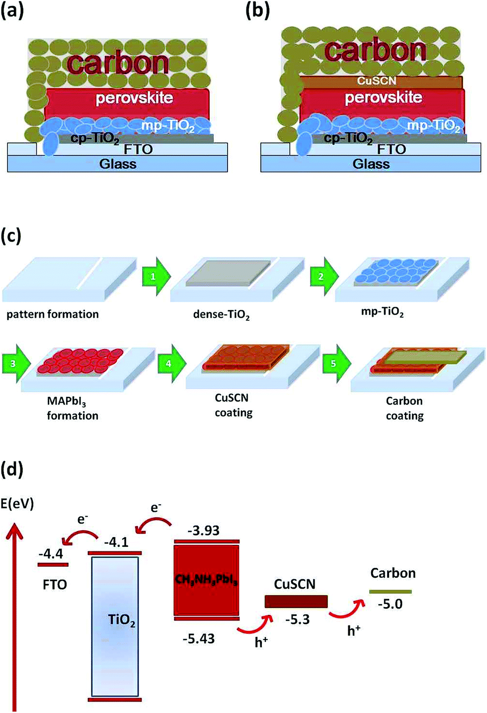 | ||
| Fig. 1 Schematic of the fabricated MAPbI3 based solar cell. (a) Carbon as the HTL and counter electrode, (b) CuSCN layer as the HTL with a carbon counter electrode, (c) a schematic of the fabrication process of the PSC, and (d) an energy diagram of the fabricated PSC. | ||
Fig. 2a and b display the cross-sectional field emission scanning electron microscopy (FESEM) images of the fabricated PSCs on different scales. The cross-section image shows that the thicknesses of mp TiO2 and MAPbI3 are around 200 and 400 nm, respectively. On the other hand, the thicknesses of CuSCN and the carbon layers are around 40 nm and 120 μm, respectively. The composition of the cross-section of the CuSCN HTL-based PSC is shown in the energy dispersive X-ray (EDX) mapping. It shows the presence of elemental copper (Cu) and sulfur (S) in its composition, characteristic of CuSCN (Fig. 2d and e). The MAPbI3 layer formation is also shown in the EDX mapping, as can be seen in Fig. 2f and g. The compositions of the glass and TiO2 are shown in Fig. 2c and h.
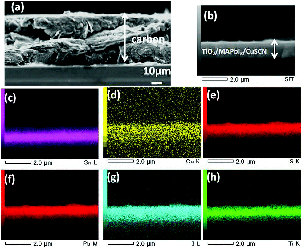 | ||
| Fig. 2 (a) The schematic FESEM images of a cross-section of the fabricated carbon/CuSCN/MAPbI3/TiO2/FTO glass-based solar cell, (b) a cross section image of the CuSCN/MAPbI3/TiO2/FTO glass in the PSC, and EDX images of (c) the tin (FTO glass) mapping, (d) the copper mapping, (e) the sulfur mapping, (f) the lead mapping, (g) the iodine mapping, and (h) the titanium (ETL) mapping. | ||
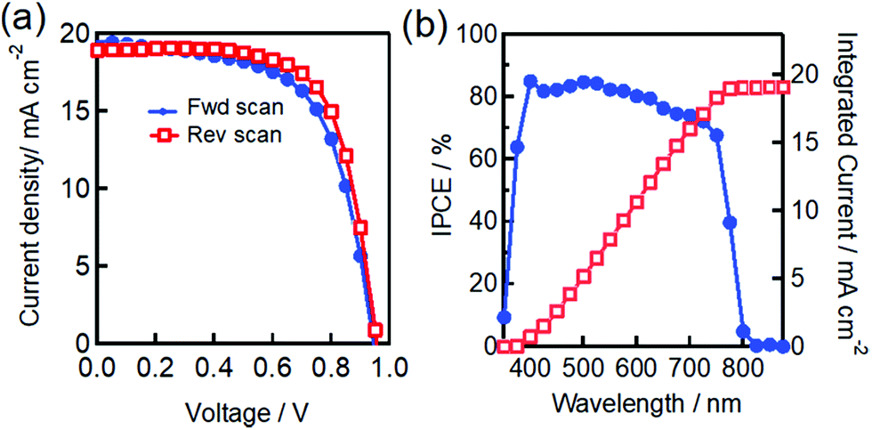
We fabricated a reference cell without the use of additional CuSCN HTL as an interface. The J–V characteristics and incident photon to current efficiency (IPCE) spectrum of the FTO/dense-TiO2/mp-TiO2/MAPbI3/carbon heterojunction PSC are shown in Fig. 3. This demonstrates the observed photovoltaic parameters of an average PCE of 10.25%, with a short circuit current density (Jsc) of 18.64 mA cm−2, an open circuit voltage (Voc) of 0.93 V, and a fill factor of 0.59 (Table 1). The integrated IPCE spectrum with solar photon flux can be employed to measure the Jsc and it was found to yield 18.53 mA cm−2, which is in close agreement with the observed Jsc shown in Table 1.
 | ||
| Fig. 3 The photovoltaic parameters measured for the FTO/dense-TiO2/mp-TiO2/MAPbI3/carbon-based PSC. (a) The J–V characteristics under 1 sun AM 1.5 conditions and (b) the IPCE spectra with integrated current density. | ||
| Parameter | Without CuSCN | With CuSCN | ||
|---|---|---|---|---|
| Reverse | Forward | Reverse | Forward | |
| J sc/mA cm−2 | 18.79 (18.42 ± 0.65) | 18.49 (18.30 ± 0.53) | 18.90 (18.74 ± 0.15) | 19.47 (19.02 ± 0.40) |
| V oc/V | 0.93 (0.94 ± 0.01) | 0.92 (0.93 ± 0.01) | 0.96 (0.96 ± 0.00) | 0.94 (0.94 ± 0.00) |
| FF | 0.63 (0.63 ± 0.00) | 0.56 (0.57 ± 0.01) | 0.68 (0.69 ± 0.00) | 0.62 (0.63 ± 0.01) |
| PCE/% | 11.15 (11.02 ± 0.43) | 9.55 (9.73 ± 0.58) | 12.41 (12.32 ± 0.09) | 11.43 (11.39 ± 0.14) |
| R s/Ω cm2 | 9.18 (9.90 ± 0.70) | 10.39 (11.04 ± 0.74) | 4.83 (4.17 ± 0.57) | 5.03 (4.39 ± 0.55) |
| R sh/Ω cm2 | 1040 (2081 ± 936) | 4990 (2520 ± 2196) | 3400 (3910 ± 1059) | 521 (794 ± 237) |
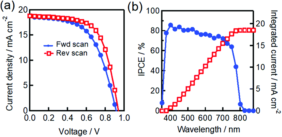
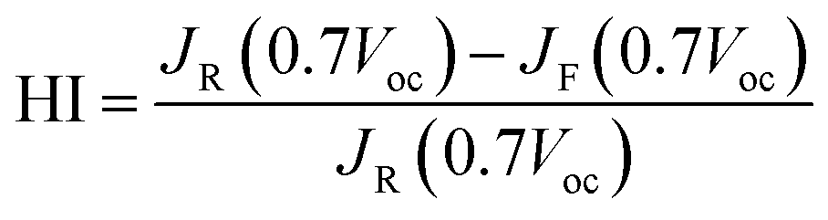
On the other hand, the J–V characteristics and IPCE of the additional CuSCN interface incorporated PSC are shown in Fig. 4. The obtained average photovoltaic parameters measured under 1 sun of simulated irradiation were a PCE of 11.92%, a Jsc of 19.19 mA cm−2, a Voc of 0.95 V and a FF of 0.65 (Table 1). The integrated Jsc value observed from the IPCE spectrum yielded 19.09 mA cm−2. The coated CuSCN layer substantially prevented direct contact between MAPbI3 and the carbon counter electrode in this modified structure. Thus, this additional interface boosted the PCE value from 10.25 to 11.92% (avg), mainly as a result of the variation of the Jsc (18.64 to 19.19 (mA cm−2)), Voc (0.93 to 0.95 (V)) and FF (0.59 to 0.65) values, speculating an improvement in the contact quality, thereby reducing possible recombination. Table 1 also shows that the resulting hysteresis effect is reduced. This notorious hysteresis effect might disappear due to the efficient charge extraction at the carbon electrode interface. The poor charge collection due to inferior contact at the interface of MAPbI3 led to a high density of charge accumulation and the resulting ion migration defect is speculated to account for the difference between the forward (fwd) and reverse (rev) scans of the J–V curves, as defined as hysteresis.37,38 In this paper, the measure of hysteresis is defined using the hysteresis index (HI):
 | ||
| Fig. 4 The photovoltaic parameters measured for the FTO/dense-TiO2/mp-TiO2/MAPbI3/CuSCN/carbon heterojunction PSC. (a) The J–V characteristics under 1 sun AM 1.5 conditions and (b) the IPCE spectra with integrated current density. | ||
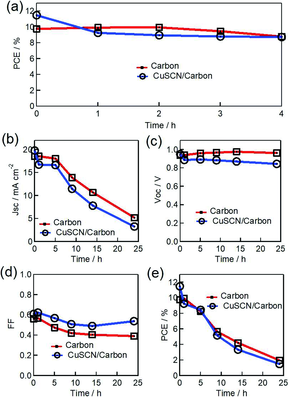
The perovskite-based photovoltaics produced so far suffer under the influence of moisture/oxygen, photo illumination, electric field and thermal stress. On the other hand, carbon has proven to be a good protective layer against primary degradation factors and increase the stability. Therefore, we checked the PSC working stability under native real conditions in a systematic way under these external factors. Firstly, we carried out dark-ambient stability tests on the fabricated unencapsulated PSCs. The fabricated PSCs were kept in the dark, under laboratory 50–70% RH conditions at ambient temperature. The observed photovoltaic parameters measured under 1 sun simulated irradiation conditions plotted in Fig. 5 show typical behavior during the shelf tests. The MAPbI3/carbon-based PSC shows remarkable stability by retaining its initial PCE (7.70%, Jsc of 18.39 mA cm−2, Voc of 0.92 V, and FF of 0.45) following 185 days of storage with 8.23% final efficiency. It is thought that the added CuSCN HTM layer functions as an additional layer to preserve the perovskite semiconductor against the possible intrusion of moisture/oxygen. However, the CuSCN inter-layer incorporated enhanced hole extraction based PSC (8.45% initial efficiency, Jsc of 19.13 mA cm−2, Voc of 0.92 V, and FF of 0.48) started to lose its initial PCE after only a hundred hours of storage and approximately 68% of the initial PCE was retained at the end of the 185 days of measurements. The reduction in the PSC performance can be mainly attributed to the loss in the Jsc and FF values, which is evident from Fig. 5. This loss in PCE may be ascribed to the modified CuSCN led interface degradation, particularly at the MAPbI3 interface.39 The degradation of the CuSCN/MAPbI3 interface was induced with time by the loss of SCN− from the thin CuSCN layer that initiated interdiffusion between the CuSCN and MAPbI3 layers. Such interface degradation of CuSCN/MAPbI3 has been observed even under controlled humidity/oxygen atmospheres.13,46 However, after this promising observed 4500 h long duration of dark stability under possible ambient exposure, it would be interesting to see the effect of light or heat as a possible external stress on the photovoltaic performance for future commercial purposes.
 | ||
| Fig. 5 Time evolution measurements of the average photovoltaic parameters of a typical unencapsulated cell stored in the dark at 50–70% RH under ambient conditions. The MAPbI3/carbon-based PSC (red line with rectangular marks) and the MAPbI3/CuSCN/carbon-based PSC (blue line with circular marks). (a) The Jsc pattern, (b) Voc pattern, (c) FF pattern, and (d) PCE pattern. All parameters were measured under 1 sun simulated irradiation. | ||
The white LED light illumination tests on ambient encapsulated PSCs were performed at a relatively high humidity of 70% under short circuit conditions. We note that the testing under these rigorous conditions is essential and natural as the outdoor atmosphere can easily achieve such conditions. Fig. 6 shows the observed photovoltaic parameters measured during the time course. The selected PSC with MAPbI3/carbon heterojunction had an initial photovoltaic performance (avg) with a Jsc of 18.52 mA cm−2, a Voc of 0.93 V, a FF of 0.56 and a PCE value of 9.76%. Finally, the measured photovoltaic performance parameters (avg) after 24 h of photon illumination stress were a Jsc of 5.2 mA cm−2, a Voc of 0.96 V, and a FF of 0.39 yielding a 1.95% PCE value, resulting in a 78% loss in the initial PCE. The devices with modified CuSCN/carbon interfaces (avg PCE parameters: Jsc of 19.79 mA cm−2, Voc of 0.95 V, FF of 0.60 and PCE of 11.45%) could also not maintain this initial performance and approx. 20% of the initial PCE value was conserved (final avg PCE parameters: Jsc of 3.28 mA cm−2, Voc of 0.84 V, FF of 0.53 and a PCE value of 1.49%).
 | ||
| Fig. 6 Time evolution measurements of the average photovoltaic parameters under light illumination stress. Cells were encapsulated at 70% RH under ambient conditions. The MAPbI3/carbon heterojunction PSC (red line with rectangular marks) and the MAPbI3/CuSCN/carbon heterojunction PSC (blue line with circular marks). (a) PCE pattern for the initial 4 h, (b) the Jsc pattern, (c) Voc pattern, (d) FF pattern, and (e) PCE pattern. All parameters were measured simultaneously under short circuit conditions and 1 sun simulated irradiation. | ||
Previously, we reported the role of a TiO2 scaffold on the photostability of a perovskite medium where a thin layer of Sb2S3 was used to prevent photodegradation.40 However, devices in this paper were encapsulated, as explained in the Experimental section, and white light was used as an illumination source to prevent UV-vis led degradation. Therefore, this prevented the possibility of the existence of infamous degrading factors such as moisture/oxygen, meaning that intrinsic factors seemed to be responsible for the losses in the J–V parameters. In terms of internal factors, ion migration and its effects remain under debate as a possible source of instability in the working of perovskite-based photovoltaics.41 Under illumination, ionic migration induced conductivity enhances many folds creating the ionic defects/vacancies, which may be a source of the cause of the damaging of the functioning of stable PSCs.42,43 These ionic vacant sites hop in a facile way to redistribute themselves under the effect of an electric field.44 The distribution of the ionic motion may become irreversible after a certain time interval, leading to a reduction in the photovoltaic performance.45 In our experiment, the MAPbI3/carbon and modified CuSCN/carbon-based solar cells retained ∼90% and ∼80% of their initial efficiencies, respectively, after 4 h of light illumination aging (Fig. 6a). The degradation effects following the 4 h photo illumination test, irrespective of the modified interface, seem to be fast leading to a severe loss in the Jsc value, as reflected in the PCE pattern (Fig. 6b). Due to the applied electric field, the resulting ion distributions inside the cell find preferential paths at respective electrodes. Therefore, an additional electron blocking inorganic CuSCN layer covering up the perovskite semiconductor may provide a barrier for possible perovskite disintegration by making a thin pinhole-free layer, but still does not preserve the PCE value. The degradation path of PSCs may include the decay of the perovskite layer, the interface material and/or their interfaces. At the end of the light shining tests, the color of the perovskite medium changed to yellow, irrespective of the interfaces (Fig. 8b and c). Interestingly, the Voc decay of the PSCs with the carbon and CuSCN/carbon electrodes showed a different pattern (Fig. 6c), suggesting that the charge distribution and recombination at the interfaces are quite different and that different degradation mechanisms of light harvesting PSC are possible, which will be a future point of discussion. The arising FF aging degradation pattern (Fig. 6d) shows a variation in the series/shunt resistance of the PSCs due to perovskite disintegration. Therefore, under the combined influence of photo-illumination and bias voltage, the irreversible migration forms a potential unharvesting yellow PbI2 medium, which arises after the migration of weakly bound CH3NH3+ ions (Fig. 8b and c). However, the possibility of the presence of residual oxygen in the sealed PSC arising from ambient sealing and its effect on the PCE parameters could not be avoided. Analysis of this is currently underway. Previously, the degradation of the MAPbI3/CuSCN interface was found to be responsible for the instability of PSCs, but here we did not observe significant interface dependency over the chosen 24 h period of light shining tests.39,46
It is quite important to confirm the ion migration in the sealed cells under light illumination. We have already demonstrated light stability tests on sealed cells of 〈glass/FTO/perovskite/carbon〉27 and ion exchange issues between the perovskite and CuSCN.47 The demonstration of light-enhanced ion migration between the perovskite and CuSCN is also important, and will be examined in future research.
Heat is another external cause, alongside moisture and photo illumination, concerning the working operation of MAPbI3 based solar cells. Therefore, here, according to IEC 61646 climate chamber test norms, 85 °C thermal stress was chosen to test the sustainability of the PSCs. PSCs were encapsulated, as detailed in the Experimental section, and were kept at 85 °C, maintained using a hot plate, under atmospheric 60–70% RH, covered with an opaque Petri dish. Fig. 7 shows the dark thermal stability J–V characteristic measurements of fabricated PSCs with MAPbI3/carbon (initial avg eff. of 10.34%) and CuSCN/carbon (initial avg eff. of 11.92%) architectures. The carbon and modified carbon-based PSCs retained their initial efficiency over 175 h of testing (Fig. 7a). However, after this time duration, the carbon-based PSC without any HTM survived the thermal stress and still retained its initial PCE after 1000 h. The thermal stability depends on all of the device components, suggesting that all of the layers are thermally stable and that the chemically inactive carbon layer can maintain the thermal stability, preventing any induced degradation. Although the MAPbI3 crystal phase transforms at 65 °C, it recovers its initial photon harvesting phase again after cooling, since PSCs were maintained under ambient conditions for 30–45 min before carrying out any PCE measurements. This observation is in accordance with the results in our previous publication, where carbon electrode-based printable monolithic PSC working was observed to be stable after 100 °C of thermal stress.26,28 Apparently, the PSC with a CuSCN modified carbon interface was not able to survive the thermal stress and experienced a loss in its initial PCE value, retaining only 17% of its initial efficiency. The degradation in the PCE value is a result of the fall in all of the photovoltaic parameters, suggesting that the instability may be related to the modified CuSCN–carbon interface. Significantly, the stable and inactive nature of the hydrophobic carbon layer further suggests that the origin of the instability is associated with the modified MAPbI3/CuSCN interface.39 It is generally accepted that CuSCN-based PSCs experience interfacial degradation problems. Following 170 h of thermal testing, all of the PCE parameters began to decrease. However, the color of the heat treated device with the CuSCN interlayer was observed to be brown (Fig. 8e). Therefore, we supposed that the CuSCN/MAPbI3 interface could not be maintained and thus this interface might be damaged. Such interface degradation has been previously observed and can be avoided by inserting a thin interface layer between CuSCN and MAPbI3.13,46 Photographs of the devices after 1000 h of 85 °C thermal stress are shown in Fig. 8d and e.
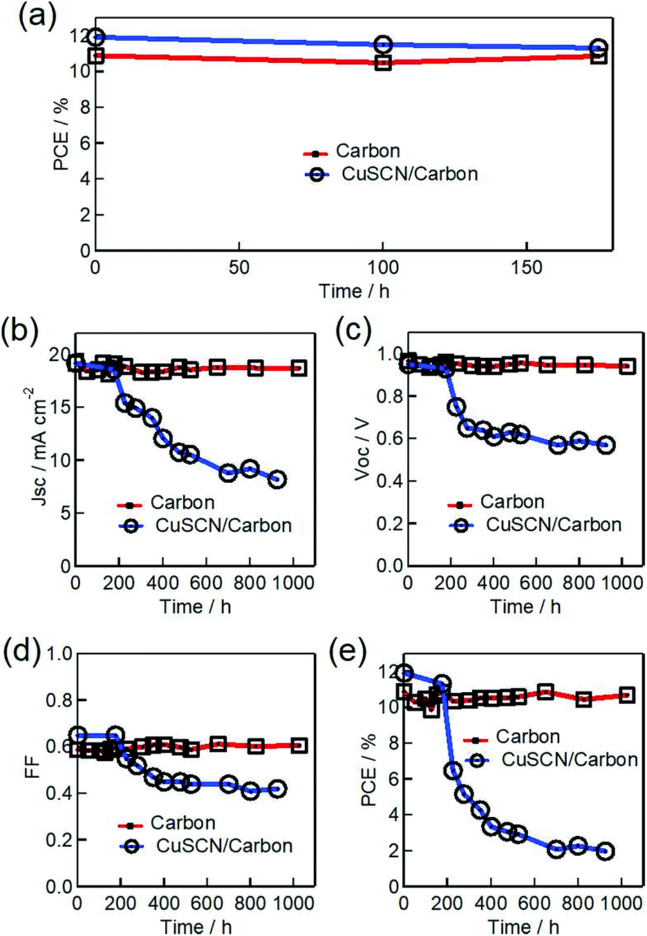 | ||
| Fig. 7 Time evolution measurements of the average photovoltaic parameters of 85 °C/dark aged, 60–70% RH, stored encapsulated devices. The MAPbI3/carbon heterojunction PSC (red line with rectangular marks) and the MAPbI3/CuSCN/carbon heterojunction PSC (blue line with circular marks). (a) The PCE pattern for the initial 170 h, (b) the Jsc pattern, (c) Voc pattern, (d) FF pattern, and (e) PCE pattern. All parameters were measured under 1 sun simulated irradiation. PSCs were kept under ambient conditions for 30–45 min before carrying out the PCE measurements. | ||
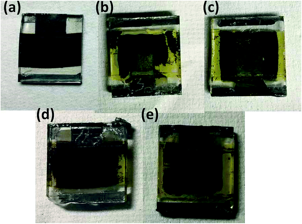 | ||
| Fig. 8 Photographs showing the typical representative PSC front view, before light/heat stress (a), after the light illumination test carried out under short-circuit conditions at an ambient 70% RH, for carbon/MAPbI3 (b) and carbon/CuSCN/MAPbI3 (c), and after 1000 h under 85 °C of external thermal stress, for the carbon/MAPbI3 (d) and, carbon/CuSCN/MAPbI3 (e) based heterojunction solar cells. | ||
The fabricated PSC architectures have similar ETLs and the only HTL interface is modified by the additional inorganic interface. Thus, comparison of these two structures shows that the fast degradation of the PCE is observed with the CuSCN interface, irrespective of the shelf, light illumination or thermal stress testing. Although the PSCs were properly encapsulated and the additional inorganic HTM and thick hydrophobic carbon layers can be used to further protect the perovskite layer, internal factors, particularly the charge and ion migration under applied stress, seem to be responsible for the degradation. However, the additional inorganic CuSCN layer underplays the stability by damaging the interface.13,39,46 Future work is underway to achieve a light illumination stable PSC utilizing an inorganic HTL with abundant carbon electrodes.
The mention of absolute values of the photovoltaic parameters is necessary to avoid the ambiguity and overestimation of the observed stability. Therefore, in this study, we show the absolute values of the PCE parameters, irrespective of the ambient dark, ambient light illumination or ambient dark thermal testing. The dark ambient-stability devices have relatively low PCEs in comparison to the normal devices, which might be due to the batch to batch variation in the observed PCEs.
Experimental
Solar cell fabrication
Fluorine-doped SnO2 (FTO) glass substrates (t = 2.2 mm) were purchased from Pilkington. FTO coated glass was laser etched by a CO2 laser beam to form two separate electrode patterns before processing the ultrasonic cleaning. The cleaning steps followed one another consecutively, with the use of detergent water, distilled water, and ethanol (Kanto Chemical Co. Inc./KCI), respectively, for 15 min each. The cleaned FTO glass substrate was subjected to UV-O3 treatment for 20 min to eliminate any organic impurities. Afterwards, the FTO glass substrates were placed on a hot plate and the temperature was raised to 500 °C and diluted titanium di-isopropoxide bis(acetylacetonate) (TAA; Sigma Aldrich, 200 μL in 7.5 mL of ethanol) was aerosol sprayed to form a dense layer of TiO2. TAA-coated FTO substrates were removed from the hot plate following a cooling down period to ambient temperature and were again subjected to UV-O3 treatment to prepare the scaffold TiO2 by spin coating diluted PST-30NRD in ethanol (1![[thin space (1/6-em)]](https://www.rsc.org/images/entities/char_2009.gif) :3.5, wt/wt) at 5000 rpm for 25 s. The substrates were dried out at 120 °C for 5 min and baked at 500 °C for 30 min, followed by 70 mM TiCl4 treatment at 70 °C for 30 min. The treated film was baked at 500 °C for 30 min in a furnace. The substrates were transferred into a N2 filled glove box for perovskite crystal formation. A 2.2 M solution (1:9/DMSO (dimethyl sulfoxide/KCI):DMF (dimethylformamide/KCI)) of a PbI2–MAI–DMF complex (Tokyo Chemical Industry Co. Ltd./TCI) preheated at 60 °C was spin coated onto the prepared TiO2 substrates using a two-step process at 500 and 6000 rpm. The anti-solvent toluene was dripped using a plastic disposable syringe 5 s before the end of the spinning in order to grow a smooth perovskite film. After this, the film was baked on a hot plate at 60 and 100 °C, each for 10 minutes, respectively. The 0.1 M CuSCN (Mitsuwa Pure Chemicals) in diethyl sulfide (TCI) was prepared by stirring overnight and was filtered using a 0.45 μm PVDF filter before use. The perovskite coated FTO glass substrates were taken out of the glove box and the filtered CuSCN solution was quickly dropped (within 2–3 s) on the spinning substrates. The spinning conditions were set at 4000 rpm for 30 s. The CuSCN coated substrate was heated at 50 °C for 10 min to remove any residual solvents. Finally, a carbon slurry coating was applied using the doctor blade method under ambient conditions followed by baking at 75 °C for 30 min. The low-temperature processed carbon slurry was prepared following the method in our previous publication.16 The fabricated PSCs were stored in the dark for at least five days to remove any residual solvents to achieve PSC stabilization and afterwards, sealing was performed under native ambient 50–70% RH, following the method in our previous publication, using an edge sealing protocol where, adhesive glue (3035B, Three Bond Holding Co. Ltd) was set onto the glass cover, and it was pressed over the carbon electrodes of the PSC so that the excess glue could evacuate to the edge. The assembly was quickly exposed to UV light (365 nm, NS-ULEDN-102CT, NS Lighting Co. Ltd) for 40 s to cure the glue.26
:3.5, wt/wt) at 5000 rpm for 25 s. The substrates were dried out at 120 °C for 5 min and baked at 500 °C for 30 min, followed by 70 mM TiCl4 treatment at 70 °C for 30 min. The treated film was baked at 500 °C for 30 min in a furnace. The substrates were transferred into a N2 filled glove box for perovskite crystal formation. A 2.2 M solution (1:9/DMSO (dimethyl sulfoxide/KCI):DMF (dimethylformamide/KCI)) of a PbI2–MAI–DMF complex (Tokyo Chemical Industry Co. Ltd./TCI) preheated at 60 °C was spin coated onto the prepared TiO2 substrates using a two-step process at 500 and 6000 rpm. The anti-solvent toluene was dripped using a plastic disposable syringe 5 s before the end of the spinning in order to grow a smooth perovskite film. After this, the film was baked on a hot plate at 60 and 100 °C, each for 10 minutes, respectively. The 0.1 M CuSCN (Mitsuwa Pure Chemicals) in diethyl sulfide (TCI) was prepared by stirring overnight and was filtered using a 0.45 μm PVDF filter before use. The perovskite coated FTO glass substrates were taken out of the glove box and the filtered CuSCN solution was quickly dropped (within 2–3 s) on the spinning substrates. The spinning conditions were set at 4000 rpm for 30 s. The CuSCN coated substrate was heated at 50 °C for 10 min to remove any residual solvents. Finally, a carbon slurry coating was applied using the doctor blade method under ambient conditions followed by baking at 75 °C for 30 min. The low-temperature processed carbon slurry was prepared following the method in our previous publication.16 The fabricated PSCs were stored in the dark for at least five days to remove any residual solvents to achieve PSC stabilization and afterwards, sealing was performed under native ambient 50–70% RH, following the method in our previous publication, using an edge sealing protocol where, adhesive glue (3035B, Three Bond Holding Co. Ltd) was set onto the glass cover, and it was pressed over the carbon electrodes of the PSC so that the excess glue could evacuate to the edge. The assembly was quickly exposed to UV light (365 nm, NS-ULEDN-102CT, NS Lighting Co. Ltd) for 40 s to cure the glue.26
Device characterization
The photovoltaic performance was measured under AM 1.5 conditions at ambient temperature using a solar simulator equipped with a 500 W xenon lamp (Yamashita Denso, Japan). The power of the simulated light was calibrated using a reference Si photodiode (Bunkou Keiki, Japan). The J–V curves were measured by applying an external bias to the PSCs and the generated photocurrents were measured with a 6240 DC current source, ADCMT, Japan. For J–V characterization, the scan speed was maintained at 50 mV s−1 and we did not use any kind of bias before the measurements. The IPCE was measured by a 300 mW xenon light source as a monochromator (M10, Bunkou Keiki). A JEOL JSM-6510 field emission scanning electron microscopy (FESEM) equipped with an energy-dispersive X-ray spectroscopy (EDS) system was employed to observe and analyze the materials. During the J–V characteristic measurements, the PSCs were covered using a black mask with a 0.16 cm2 active open area. Light stability tests were measured under ambient 70% RH using a white LED lamp.Conclusions
In summary, we incorporated an additional inorganic CuSCN layer at the interface of MAPbI3/carbon to promote favorable energy matching for easy hole extraction and enhanced photovoltaic performance was realized. Dark stability tests of the fabricated unencapsulated PSCs were performed, and the FTO/dense-TiO2/mp-TiO2/MAPbI3/carbon and FTO/dense-TiO2/mp-TiO2/MAPbI3/CuSCN/carbon-based PSCs retained 94% and 74% of their initial PCE values, respectively. The light illumination testing of these encapsulated PSCs was also performed at ambient 70% RH. At the end of 24 h of light illumination tests, both of these PSC structures were able to retain 22% and 20% of their initial PCE values, respectively. The thermal stress (85 °C) tests of these encapsulated PSCs resulted in stable PCE values for MAPbI3/carbon and 17% of the initial PCE values were retained for the MAPbI3/CuSCN/carbon devices. The incorporated inorganic CuSCN layer in the MAPbI3–carbon interface based devices showed fast PCE degradation, but the use of another stable inorganic HTM or tunneling layer is needed among the MAPbI3/carbon to help the system to cope with external stress.Conflicts of interest
There are no conflicts to declare.Acknowledgements
Authors would like to express sincere thanks to the Advanced Low Carbon Technology Research and Development Program (ALCA-JST), Japan.References
- A. Kojima, K. Teshima, Y. Shirai and T. Miyasaka, Organometal Halide Perovskites as Visible-Light Sensitizers for Photovoltaic Cells, J. Am. Chem. Soc., 2009, 131, 6050–6051 CrossRef CAS PubMed.
- H.-S. Kim, C.-R. Lee, J.-H. Im, K.-B. Lee, T. Moehl, A. Marchioro, S.-J. Moon, R. Humphry-Baker, J.-H. Yum, J. E. Moser, M. Grätzel and N.-G. Park, Lead Iodide Perovskite Sensitized All-Solid-State Submicron Thin Film Mesoscopic Solar Cell with Efficiency Exceeding 9%, Sci. Rep., 2012, 2, 591 CrossRef PubMed.
- W. S. Yang, B.-W. Park, E. H. Jung, N. J. Jeon, Y. C. Kim, D. U. Lee, S. S. Shin, J. Seo, E. K. Kim, J. H. Noh and S. Il Seok, Iodine management in formamidinium-lead-halide based perovskite layers for efficient perovskite solar cells, Science, 2017, 356, 1376–1379 CrossRef CAS PubMed.
- S. Ito, Research Update: Overview of progress about efficiency and stability on perovskite solar cells, APL Mater., 2016, 4, 091504 CrossRef.
- H.-S. Kim, J.-Y. Seo and N.-G. Park, Material and Device Stability in Perovskite Solar Cells, ChemSusChem, 2016, 9, 2528–2540 CrossRef CAS PubMed.
- S. D. Stranks, G. E. Eperon, G. Grancini, C. Menelaou, M. J. P. Alcocer, T. Leijtens, L. M. Herz, A. Petrozza and H. J. Snaith, Electron-Hole Diffusion Lengths Exceeding 1 Micrometer in an Organometal Trihalide Perovskite Absorber, Science, 2013, 342, 341–344 CrossRef CAS PubMed.
- Q. Dong, Y. Fang, Y. Shao, P. Mulligan, J. Qiu, L. Cao and J. Huang, Electron-hole diffusion lengths >175 μm in solution-grown CH3NH3PbI3 single crystals, Science, 2015, 347, 967–970 CrossRef CAS PubMed.
- G. Xing, N. Mathews, S. Sun, S. S. Lim, Y. M. Lam, M. Gratzel, S. Mhaisalkar and T. C. Sum, Long-Range Balanced Electron- and Hole-Transport Lengths in Organic-Inorganic CH3NH3PbI3, Science, 2013, 342, 344–347 CrossRef CAS PubMed.
- L. Calió, S. Kazim, M. Grätzel and S. Ahmad, Hole-Transport Materials for Perovskite Solar Cells, Angew. Chem., Int. Ed., 2016, 55, 14522–14545 CrossRef PubMed.
- W. Li, H. Dong, L. Wang, N. Li, X. Guo, J. Li and Y. Qiu, Montmorillonite as bifunctional buffer layer material for hybrid perovskite solar cells with protection from corrosion and retarding recombination, J. Mater. Chem. A, 2014, 2, 13587–13592 RSC.
- P. Qin, S. Tanaka, S. Ito, N. Tetreault, K. Manabe, H. Nishino, M. K. Nazeeruddin and M. Grätzel, Inorganic hole conductor-based lead halide perovskite solar cells with 12.4% conversion efficiency, Nat. Commun., 2014, 5, 1–6 Search PubMed.
- S. Ito, S. Tanaka, H. Vahlman, H. Nishino, K. Manabe and P. Lund, Carbon double bond free printed solar cells from TiO2/CH3NH3PbI3/CuSCN/Au: Structural Control and Photoaging Effects, ChemPhysChem, 2014, 15, 1194–1200 CrossRef CAS PubMed.
- N. Arora, M. I. Dar, A. Hinderhofer, N. Pellet, F. Schreiber, S. M. Zakeeruddin and M. Grätzel, Perovskite solar cells with CuSCN hole extraction layers yield stabilized efficiencies greater than 20%, Science, 2017, 358, 768–771 CrossRef CAS PubMed.
- J. A. Christians, R. C. M. Fung and P. V. Kamat, An Inorganic Hole Conductor for Organo-Lead Halide Perovskite Solar Cells. Improved Hole Conductivity with Copper Iodide, J. Am. Chem. Soc., 2014, 136, 758–764 CrossRef CAS PubMed.
- C. Zuo and L. Ding, Solution-Processed Cu2O and CuO as Hole Transport Materials for Efficient Perovskite Solar Cells, Small, 2015, 11, 5528–5532 CrossRef CAS PubMed.
- T. A. N. Peiris, A. K. Baranwal, H. Kanda, S. Fukumoto, S. Kanaya, L. Cojocaru, T. Bessho, T. Miyasaka, H. Segawa and S. Ito, Enhancement of the Hole Conducting Effect of NiO by N2 Blow Drying Method in Printable Perovskite Solar Cells with Low-Temperature Carbon as the Counter Electrode, Nanoscale, 2017, 9, 5475–5482 RSC.
- K. Domanski, J.-P. Correa-Baena, N. Mine, M. K. Nazeeruddin, A. Abate, M. Saliba, W. Tress, A. Hagfeldt and M. Grätzel, Not All That Glitters Is Gold: Metal-Migration-Induced Degradation in Perovskite Solar Cells, ACS Nano, 2016, 10, 6306–6314 CrossRef CAS PubMed.
- C. Besleaga, L. E. Abramiuc, V. Stancu, A. G. Tomulescu, M. Sima, L. Trinca, N. Plugaru, L. Pintilie, G. A. Nemnes, M. Iliescu, H. G. Svavarsson, A. Manolescu and I. Pintilie, Iodine Migration and Degradation of Perovskite Solar Cells Enhanced by Metallic Electrodes, J. Phys. Chem. Lett., 2016, 7, 5168–5175 CrossRef CAS PubMed.
- H. Chen and S. Yang, Carbon-Based Perovskite Solar Cells without Hole Transport Materials: The Front Runner to the Market?, Adv. Mater., 2017, 29, 1603994 CrossRef PubMed.
- H. Chen and S. Yang, Stabilizing and scaling up carbon-based perovskite solar cells, J. Mater. Res., 2017, 32, 3011–3020 CrossRef CAS.
- W. J. Lee, E. Ramasamy, D. Y. Lee and J. S. Song, Performance variation of carbon counter electrode based dye-sensitized solar cell, Sol. Energy Mater. Sol. Cells, 2008, 92, 814–818 CrossRef CAS.
- X. Wang, L. Zhi, N. Tsao, Ž. Tomović, J. Li and K. Müllen, Transparent Carbon Films as Electrodes in Organic Solar Cells, Angew. Chem., Int. Ed., 2008, 47, 2990–2992 CrossRef CAS PubMed.
- Z. Ku, Y. Rong, M. Xu, T. Liu and H. Han, Full Printable Processed Mesoscopic CH3NH3PbI3/TiO2 Heterojunction Solar Cells with Carbon Counter Electrode, Sci. Rep., 2013, 3, 3132 CrossRef PubMed.
- A. Mei, X. Li, L. Liu, Z. Ku, T. Liu, Y. Rong, M. Xu, M. Hu, J. Chen, Y. Yang, M. Gratzel and H. Han, A hole-conductor–free, fully printable mesoscopic perovskite solar cell with high stability, Science, 2014, 345, 295–298 CrossRef CAS PubMed.
- G. Grancini, C. Roldán-Carmona, I. Zimmermann, E. Mosconi, X. Lee, D. Martineau, S. Narbey, F. Oswald, F. De Angelis, M. Graetzel and M. K. Nazeeruddin, One-Year stable perovskite solar cells by 2D/3D interface engineering, Nat. Commun., 2017, 8, 15684 CrossRef CAS PubMed.
- A. K. Baranwal, S. Kanaya, T. A. N. Peiris, G. Mizuta, T. Nishina, H. Kanda, T. Miyasaka, H. Segawa and S. Ito, 100 C Thermal Stability of Printable Perovskite Solar Cells Using Porous Carbon Counter Electrodes, ChemSusChem, 2016, 9, 2604–2608 CrossRef CAS PubMed.
- S. Ito, G. Mizuta, S. Kanaya, H. Kanda, T. Nishina, S. Nakashima, H. Fujisawa, M. Shimizu, Y. Haruyama and H. Nishino, Light stability tests of CH3NH3PbI3 perovskite solar cells using porous carbon counter electrodes, Phys. Chem. Chem. Phys., 2016, 18, 27102–27108 RSC.
- S. Ito, A. K. Baranwal, H. Kanda, N. Shibayama, H. Masutani, T. A. N. Peiris, S. Kanaya, H. Segawa and T. Miyasaka, Thermal Degradation Analysis of Sealed Perovskite Solar Cell with Porous Carbon Electrode at 100 °C for 7000 h, Energy Technol., 2018 DOI:10.1002/ente.201800572.
- Z. Liu, T. Shi, Z. Tang, B. Sun and G. Liao, Using low-temperature carbon electrode for preparing holeconductor- free perovskite heterojunction solar cells under high relative humidity, Nanoscale, 2016, 8, 7017–7023 RSC.
- H. Zhou, Y. Shi, K. Wang, Q. Dong, X. Bai, Y. Xing, Y. Du and T. Ma, Low-Temperature Processed and Carbon-Based ZnO/CH3NH3PbI3/C Planar Heterojunction Perovskite Solar Cells, J. Phys. Chem. C, 2015, 119, 4600–4605 CrossRef CAS.
- Z. Wei, X. Zheng, H. Chen, X. Long, Z. Wang and S. Yang, A Multifunctional C+epoxy/Ag-paint Cathode Enables Efficient and Stable Operation of Perovskite Solar Cells in Watery Environments, J. Mater. Chem. A, 2015, 3, 16430–16434 RSC.
- J. Li, G. Niu, W. Li, K. Cao, M. Wang and L. Wang, Insight into the CH3NH3PbI3/C interface in hole-conductor-free mesoscopic perovskite solar cells, Nanoscale, 2016, 8, 14163–14170 RSC.
- X. Jiang, Z. Yu, Y. Zhang, J. Lai, J. Li, G. G. Gurzadyan, X. Yang and L. Sun, High-Performance Regular Perovskite Solar Cells Employing Low-Cost oly(ethylenedioxythiophene) as a Hole-Transporting Material, Sci. Rep., 2017, 7, 42564 CrossRef CAS PubMed.
- J. Ryu, K. Lee, J. Yun, H. Yu, J. Lee and J. Jang, Paintable Carbon-Based Perovskite Solar Cells with Engineered Perovskite/Carbon Interface Using Carbon Nanotubes Dripping Method, Small, 2017, 13, 1701225 CrossRef PubMed.
- Y. Zhang, X. Zhuang, K. Zhou, C. Cai, Z. Hu, J. Zhang and Y. Zhu, Vibration treated carbon electrode for highly efficient hole-conductor-free perovskite solar cells, Org. Electron., 2018, 52, 159–164 CrossRef CAS.
- M. Jung, Y. C. Kim, N. J. Jeon, W. S. Yang, J. Seo, J. H. Noh and S. Il Seok, Thermal Stability of CuSCN Hole Conductor-Based Perovskite Solar Cells, ChemSusChem, 2016, 9, 2592–2596 CrossRef CAS PubMed.
- B. Wu, K. Fu, N. Yantara, G. Xing, S. Sun, T. C. Sum and N. Mathews, Charge Accumulation and Hysteresis in Perovskite-Based Solar Cells: An Electro-Optical Analysis, Adv. Energy Mater., 2015, 5, 1500829 CrossRef.
- D.-Y. Son, S.-G. Kim, J.-Y. Seo, S.-H. Lee, H. Shin, D. Lee and N.-G. Park, Universal Approach toward Hysteresis-Free Perovskite Solar Cell via Defect Engineering, J. Am. Chem. Soc., 2018, 140, 1358–1364 CrossRef CAS PubMed.
- J. Chen, J.-Y. Seo and N.-G. Park, Simultaneous Improvement of Photovoltaic Performance and Stability by In Situ formation of 2D Perovskite at (FAPbI3)0.88(CsPbBr3)0.12/CuSCN Interface, Adv. Energy Mater., 2018, 8, 1702714 CrossRef.
- S. Ito, S. Tanaka, K. Manabe and H. Nishino, Effects of Surface Blocking Layer of Sb2S3 on Nanocrystalline TiO2 for CH3NH3PbI3 Perovskite Solar Cells, J. Phys. Chem. C, 2014, 118, 16995–17000 CrossRef CAS.
- Y. Yuan and J. Huang, Ion Migration in Organometal Trihalide Perovskite and Its Impact on Photovoltaic Efficiency and Stability, Acc. Chem. Res., 2016, 49, 286–293 CrossRef CAS PubMed.
- G. Y. Kim, A. Senocrate, T.-Y. Yang, G. Gregori, M. Grätzel and J. Maier, Large tunable photoeffect on ion conduction in halide perovskites and implications for photodecomposition, Nat. Mater., 2018, 17, 445–449 CrossRef CAS PubMed.
- J. Xing, Q. Wang, Q. Dong, Y. Yuan, Y. Fang and J. Huang, Ultrafast ion migration in hybrid perovskite polycrystalline thin films under light and suppression in single crystals, Phys. Chem. Chem. Phys., 2016, 18, 30484–30490 RSC.
- S. Bae, S. Kim, S.-W. Lee, K. J. Cho, S. Park, S. Lee, Y. Kang, H.-S. Lee and D. Kim, Electric-Field-Induced Degradation of Methylammonium Lead Iodide Perovskite Solar Cells, J. Phys. Chem. Lett., 2016, 7, 3091–3096 CrossRef CAS PubMed.
- K. Domanski, B. Roose, T. Matsui, M. Saliba, S.-H. Turren-Cruz, J.-P. Correa-Baena, C. R. Carmona, G. Richardson, J. M. Foster, F. De Angelis, J. M. Ball, A. Petrozza, N. Mine, M. K. Nazeeruddin, W. Tress, M. Grätzel, U. Steiner, A. Hagfeldt and A. Abate, Migration of cations induces reversible performance losses over day/night cycling in perovskite solar cells, Energy Environ. Sci., 2017, 10, 604–613 RSC.
- J. Liu, S. K. Pathak, N. Sakai, R. Sheng, S. Bai, Z. Wang and H. J. Snaith, Identification and Mitigation of a Critical Interfacial Instability in Perovskite Solar Cells Employing Copper Thiocyanate Hole-Transporter, Adv. Mater. Interfaces, 2016, 3, 1600571 CrossRef.
- S. Ito, S. Kanaya, H. Nishino, T. Umeyama and H. Imahori, Material Exchange Property of Organo Lead Halide Perovskite with Hole-Transporting Materials, Photonics, 2015, 2(4), 1043–1053 CrossRef CAS.
| This journal is © The Royal Society of Chemistry 2018 |