
 Open Access Article
 This Open Access Article is licensed under a Creative Commons Attribution-Non Commercial 3.0 Unported Licence
TiOx electrode interface modification layer promises the prominent electrical/macroscopic properties of the metallized dielectric films
Qi Dong ab,
Hao-Lin Lic,
Zhong-Ming Zhua,
De-Peng Konga,
Shao-Long Zhongb and
Zhi-Min Dang*b
ab,
Hao-Lin Lic,
Zhong-Ming Zhua,
De-Peng Konga,
Shao-Long Zhongb and
Zhi-Min Dang*b
aCollege of Education, Zhejiang University of Technology, Hangzhou 310023, China
bState Key Laboratory of Power System Operation and Contral, Department of Electrical Engineering, Tsinghua University, Beijing 100084, China. E-mail: dangzm@tsinghua.edu.cn
cSchool of Materials Science and Engineering, Zhejiang Sci-Tech University, Hangzhou 310018, China
First published on 28th February 2025
Abstract
BOPP (Biaxially Oriented Polypropylene)//TiOx/Al composite films with “laminated” structure were prepared by vacuum evaporation and layer-by-layer coating. The microstructure of composite film was studied by XRD and TEM, and the interface characteristics of composite electrode were also studied by AES, while the pure Al metallized films were used as the comparison. The effect of the intermediate interlayer of BOPP/TiOx nanocomposite films on the electrical properties of the metallized films was systematically studied by characterizing the self-healing and through-current ability of the modified composite films, e.g., It was found that the wettability between the metal electrode and the dielectric film of the modified dielectric film had been apparently regulated due to the insertion of the metal oxide on its surface, which generated not merely the reduced threshold thickness of the Al electrode, and also increased through-current ability of the metallized film. Moreover, it was observed that the metallized film with TiOx interfacial layer could prevent the occurrence of transcending self-healing when it occurred, which achieved the isolating self-healing. The nanoindentation result also showed that the bonding strength between the metal electrode and the dielectric film was also improved significantly.
1. Introduction
Metallized film capacitors (MFCs) are known for significantly increasing energy density by reducing electrode thickness. However, the vapor-deposited electrode layer on the film is prone to fracturing under high-amplitude currents.1–3 Current research mainly focuses on the strategies involving the design of electrode thickness,4,5 elemental composition,6,7 and electrode patterning (or safety film).8,9 These technologies have been applied to the fabrication of organic film capacitors. Broadly, a thinner metallization layer is much more expected to foster the self-healing process in capacitors due to the harder self-healing behavior under AC (alternating current) voltages, making the further descent in the thickness of the metallization layer much more urgent.10–14Interfacial modification has been extensively accepted as an effective method to significantly reduce the threshold thickness of electrodes owing to the introduced unique interlayer-interface structure, which confers the enhanced electrical properties on the materials.15 Recently, multilayer materials have garnered widespread attention in the surface engineering community, with fabrication of composite electrodes also extensively employed in film electrode processing. This also involves augmenting the surface and interface of the electrode materials, such as, reducing the size of metal particles, incorporating porous or hierarchical structures, and modifying or functionalizing surfaces with various nanoparticles (e.g., metal, metal oxides, carbon materials, and ionic/electronic conductive polymers).16–19 While a significant amount of research has focused on the role of interfacial modification in improving the energy storage and electrical performance of metallized films, its influence on self-healing characteristics has been largely overlooked.
Due to their excellent electrical insulation and high thermal conductivity, metal oxides can be attached onto the surface of polypropylene films to form a composite insulating medium by vapor deposition. The approach is deemed effective not only in modestly increasing the relative permittivity of the composite films but also in significantly enhancing the thermal conductivity of the capacitor core.20,21 Though the rapid dissipation of heat generates from the dielectric loss or self-healing of the capacitor, the composite films are believed to prevent the interlayer adhesion of the dielectric film near the self-healing point, thereby serving an isolating function in the self-healing process.22,23
2. Experimental details
For the deposition of the titanium oxide nanofunctional layer, pure titanium metal (purity: ≥99.999%) was hereby utilized as the raw material. This vapor deposition process was executed on the BOPP-film substrate with a micrometer-scale thickness, as depicted in Fig. 1. The evaporation source was heated until adequate titanium vapor was deposited onto the film substrate. Subsequently, the vacuum supply was ceased to facilitate the titanium to react with oxygen during the vapor deposition process, so that the titanium oxide film could be obtained, and the TiO2 and Al layers were deposited sequentially without opening the deposition chamber. The pure aluminum metal was then employed as the evaporation source, which, after reestablishing the vacuum, was heated beyond 1400 °C using a resistance wire. Following that, the vaporized metal was deposited onto the titanium oxide functional layer to fulfill the fabrication of the multilayer composite electrode (Table 1). | ||
| Fig. 1 Schematic diagram of vacuum evaporation device. | ||
| Sample no. | Experimental parameters | |||
|---|---|---|---|---|
| Ti thickness (nm) | Al thickness (nm) | Evaporation velocity (Å s−1) | Vacuum level (Pa) | |
| 1 | 0 | 20 | 1 ± 0.05 | 5 × 10⁻⁴ |
| 2 | 5 | 20 | 1 ± 0.05 | 5 × 10⁻⁴ |
| 3 | 10 | 20 | 1 ± 0.05 | 5 × 10⁻⁴ |
| 4 | 20 | 20 | 1 ± 0.05 | 5 × 10⁻⁴ |
Pure titanium is particularly susceptible to forming an oxide film at high temperatures due to its chemical activity. It can even oxidize to form a 10 Å-thick oxide film within milliseconds of exposure to room temperature environment, and approximately 100 Å after 1 minute.24 In order to validate the composition of the titanium oxide electrode prepared through evaporation at room temperature, a comparison was made with the titanium oxide standard (PDF card number JCPDS No. 75-1582, with lattice constants a = 0.9184 nm, b = 0.5447 nm, and c = 0.5145 nm). The sample diffraction peaks at 25.3 and 25.7° corresponded to the (210) and (111) crystal planes of TiO2 respectively (see Fig. 2), suggesting the presence of titanium oxide components in the surface of the metallic film during the evaporation process. Indeed, further characterizations should also be conducted to determine the specific thickness.
 | ||
| Fig. 2 X-ray diffraction spectra of composite electrodes. | ||
3. Results and discussion
3.1. Enhancement of the metal electrode film quality via the modification layer
As depicted in Fig. 3 and 4, the surface of the metallized film presents a relatively smooth texture when the thickness of the composite electrode reaches approximately 40 nm. It has a comparable roughness depth (RZ) to that of the pure Al electrode, but it appears narrower and more symmetrical. Given that the titanium oxide and Al share the similar surface energies, the former is considered to promote the growth of the latter through more effective wetting. Consequently, the Al electrodes growing on the metal oxide surface during the insertion process are obviously smoother compared to those growing exclusively on the BOPP surface (Table 2). | ||
| Fig. 3 Surface morphology with different metallized dielectric films: (a) Al electrode; (b) composite electrodes. | ||
 | ||
| Fig. 4 Histogram of the surface-height values with different metallized dielectric films. | ||
| Film | Peak-to-valley roughness (nm) | RMS roughness (nm) | Image surface area difference (%) |
|---|---|---|---|
| Al | 1.316 | 1.644 | 1.31 |
| TiOx + Al | 1.045 | 0.595 | 0.912 |
3.2. Element distribution of the modification layer and interface layers
Fig. 5 presents the TEM image of the cross-section of the metallized film of the multilayer composite electrode with the BOPP serving as the dielectric film. As shown in the figure, the first dark layer in the TEM image is TiO2, approximately 12 nm thick. The transition region indicated by the arrow could potentially be interface between TiO2 and Al. Notably, clear interface regions can be observed between the dielectric film, oxide functional layer, and Al electrode layer. Besides, the second layer (gray) on the right panel with a thickness of approximately 20 nm is the metal Al layer, culminating in a total of two layers in the multi-layered film.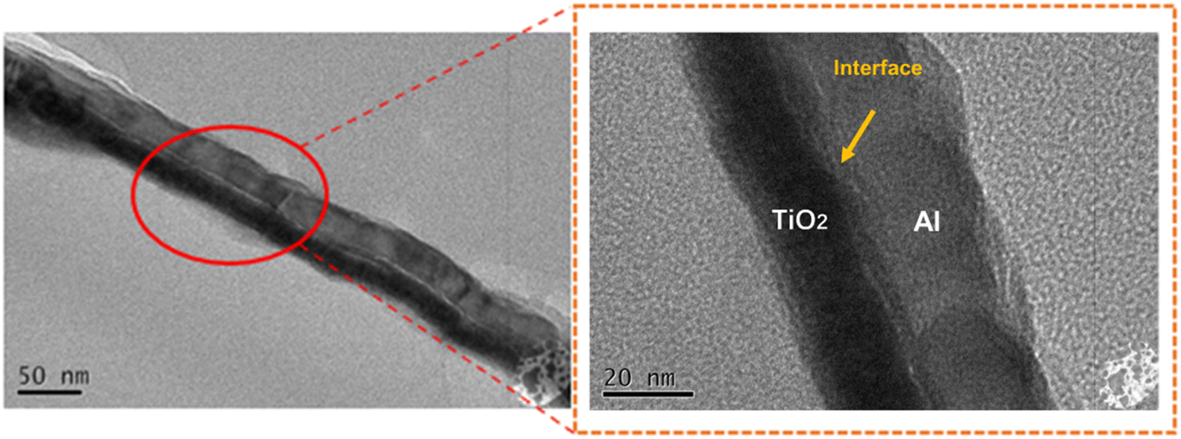 | ||
| Fig. 5 TEM bright field image of the cross section of metallized film with multilayer composite electrode. | ||
Fig. 6 obviously reveals that the initial Ti metal layer of the metallized electrode layer grows well with a flat interface, where some bent interfaces come to light as the metal layers continue to stack. The EDS analysis involving the representative surface zone yields the elemental distribution maps, as shown in Fig. 6(a) and (b), where it can be observed that the composition of Al, Ti, and O elements adhere to a distinct multilayer distribution, aligning with the intended design scheme of the multilayer film structure. However, possibly due to the oxidation of Ti metal layer during the preparation process, the O element does not seem to follow the above laminated distribution pattern, that is, partially rough surfaces on the ultra-thin metal electrode is considered to cause the oxidation layer with an inconspicuous layered pattern in the metallized electrode layer, thereby resulting in the indistinctive elemental separation between different layers.
 | ||
| Fig. 6 (a) EDS element distribution spectra of composite electrode cross sections; (b) different element content in composite electrode section. | ||
Besides the element distribution of the multilayer metallized electrode, the diffusion depth in the interface layer of the composite electrode is also thought to profoundly affect the electrical performance of the device. According to relevant studies, an increase in the diffusion depth could cause the degradation of the electrical performance for the electrode, macroscopically resulting in the device failure. Upon deposition onto a clean surface with an equal active metal dial, the depth of metal diffusion into the polymer can be achieved. The study suggests that a higher evaporation rate results in a lower depth of the metal diffusion. This occurs because the increased evaporation rate accelerates the clustering of metal on polymer surfaces, inhibiting further inward diffusion of metal elements.25
During the electrode deposition process, the evaporated particles engage in the chemical reactions with the dielectric film, reaching the depth of approximately 3–5 nm. The auger electron spectroscopy (AES) is widely recognized to be capable of precisely determining the elemental composition around the involving interfaces, which can not only illuminate the mechanisms behind interface diffusion but also aids in identifying the final products resulting from interface reactions. Herein, the elemental depth distribution curves for both Al and Ti/Al electrodes were assessed using a scanning auger nanoprobe (SAN, model PHI-700, manufactured by ULVAC-PHI, Japan). Fig. 7(a) illustrates the depth distribution curve for Al elements, wherein a sudden alteration in the curve slope signifies the interface region between the Al electrode and the substrate. It becomes apparent that some aluminum atoms have diffused into the dielectric film substrate, where the aluminum atomic percentage is observed to change gradually rather than decrease abruptly. This suggests effective atomic integration between aluminum and the BOPP substrate, indicating stronger binding. Fig. 7(b) presents the depth distribution curve for Ti/Al. Obviously, the Al element curve at the Ti/Al-BOPP interface is considerably steeper than that at the Al-BOPP interface in Fig. 7(a). Nevertheless, the Ti content curve in Fig. 7(b) changes more slowly, implying that the metal atoms in the Ti/Al electrode diffuse shallower than those in the pure Al electrode. Meanwhile, depth profiling analysis using AES has uncovered significant interfacial diffusion between Ti and the BOPP substrate during the coating process, which inhibits the Al diffusion into the film substrate. This phenomenon can be attributed to the evaporation deposition process, where the evaporation temperature of titanium and a partial implantation effect triggered by aluminum atoms bombarding the film surface facilitate easier diffusion of titanium into the PP substrate. Given the nature of the interfacial diffusion reactions involves the collision between metal atoms and the dielectric film substrate, the increase in the evaporation rate could enhance the interface diffusion of the BOPP. However, for BOPP, which is sensitive to high temperatures, excessively elevated evaporation temperatures could cause the film to deform, leading to a significant reduction in the through-flow characteristics of the electrode.
 | ||
| Fig. 7 Element depth distribution curve of nanocomposite film electrode: (a) Al electrode; (b) composite electrodes. | ||
3.3. Improvement on the electrical properties of metallized dielectric films by the modification layers
As illustrated in Fig. 8, the four-probe sheet resistance test outcomes present the similar change trends of conductivity regarding the 20 nm-thick Al electrodes and composite electrodes across diverse substrate surfaces. Despite the film type, the sheet resistance of the composite films is consistently lower than that of the pure Al electrode. At a thickness of 20 nm for the Al metallization layer, the sheet resistance of the composite electrode fabricated on the PP substrate reduces by approximately 30% in comparison to the Al electrode. Simultaneously, the sheet resistance of the electrodes on the PET (polyethylene terephthalate) and PI (polyimide) substrates decreases by nearly 50%. When the threshold thickness reaches 20 nm for the Al electrode, the composite electrode further diminishes the threshold thickness of the Al electrode. Combining the data on roughness suggests that peak-valley roughness significantly influences resistivity in the case of continuous metal electrode. Specifically, as peak-valley roughness decreases, resistivity correspondingly drops. | ||
| Fig. 8 Comparison of sheet resistivity for Al films with different substrates. | ||
Studies have confirmed that when a Schottky contact forms between a metal and an organic semiconductor, the barrier diminishes with a forward-biased external electric field from the semiconductor towards the metal. Conversely, reversing the bias heightens the barrier, providing the metal–semiconductor interface with rectification function. The incorporation influence of a titanium oxide functional layer on the dielectric constant and loss of the metallized film is depicted in Fig. 9. When the thickness of titanium oxide is approximately 5 nm, no change can be virtually observed in the dielectric constant of the metallized film in comparison with that of the pure Al electrode. On the contrary, as the thickness of the titanium oxide functional layer elevates, a corresponding increase in the dielectric constant of the BOPP can be observed. For instance, compared to a metallized film without the titanium oxide functional layer, the dielectric constant of the 20 nm composite electrode metallized film escalates from 3.65 to 3.9.
 | ||
| Fig. 9 (a) Dielectric constants of composite electrode dielectric films with different thicknesses; (b) dielectric loss of different nano-composite electrode dielectric films. | ||
Fig. 10 displays the morphology of the self-healing points associated with various metallized films. As shown in the figure, both the pure Al metallized BOPP film and composite electrode film exhibit self-healing properties, where the self-healing area of the composite films is significantly smaller than that of their pure Al counterpart. Meanwhile, the thicker the nanofunctional layer, the smaller the area of the self-healing breakdown point becomes, suggesting that the titanium oxide nanofunctional layer can mitigate the energy produced during the self-healing process of the metallized electrode. This phenomenon might be attributed to the excellent thermal conductivity of titanium oxide. On the one hand, the heat generated during the breakdown of the polymer film can be effectively transmitted to the electrode, thereby facilitating successful self-healing of the composite films, while on the other, part of the self-healing energy is utilized to clear the nanofunctional layer apart from the clearance of the metal electrode and polymer film. Such a behavior consequently curtails the energy designated for clearing the metal electrode and polymer film, resulting in a diminished self-healing point area. Revisiting the findings from the previous chapter, the oxide functional layer is believed to reduce the sheet resistance of Al electrodes sharing the same thickness, while the current-carrying capability of the metal electrode can be enhanced, which is also considered to contribute to the improvement of the self-healing properties regarding the metallized electrode.
 | ||
| Fig. 10 Self-healing radius of metallized films. | ||
3.4. Mechanical behaviors and interface characteristics of the metallized dielectric film
Herein, the critical load in Fig. 11 was determined by plotting the scratch distance from the nanoindentation test as the x-axis against the lateral force on the sample as the y-axis. The key transition point, where the friction force curve shifts from smooth to significantly fluctuating, indicates the delamination point of the film, while the corresponding load at this point is defined as the critical load. As shown in the figure, the scratch morphology appears strikingly coherent, and there is no obvious turning point observed in the corresponding friction force with modest fluctuations as the scratch distance changes. These observations further support the notion that the adhesion between the composite electrode and the BOPP film is exceptionally strong. Specifically, the composite electrode undergoes some plastic deformation (as depicted in Fig. 11), but no delamination is observed from the film surface. Combined with the previous analysis of the diffusion depth of metal atoms on the film surface, the result systematically demonstrates that the wettability between the metal oxide and the PP substrate is superior to that of a single Al electrode. This leads to excellent atomic fusion, and consequently, stronger bonding strength. | ||
| Fig. 11 Scratch test: (a) scratch morphology; (b) the curve of friction with the distance drawn. | ||
4. Conclusions
The results indicate that the introduction of the metal oxides into the modified dielectric film surface can significantly alter the wettability between the metal electrode and the dielectric film. Meanwhile, the nano-indentation measurements corroborate that the bond strength between the metal electrode and the dielectric film has been further strengthened. Additionally, the TiO2 is also found to enhance the dielectric constant and through-current ability of the metallized electrode.Specifically, the utilization of the thermal evaporation method with titanium (Ti) as the evaporation material allows for the deposition of a continuous nano-functional layer, chemically akin to titanium oxide, on the BOPP film under non-vacuum conditions. This process is verified to attenuate the threshold thickness of pure Al electrodes.
Besides, in comparison to the pure BOPP metallized film, the titanium oxide composite metallized film exhibits lower sheet resistance at an equivalent thickness, thereby augmenting the through-current ability of the metallized electrodes. Thus, a remarkable improvement in the adhesion and self-healing abilities of the metal layer can be observed.
Overall, the present results demonstrate that owing to the high thermal conductivity and high melting point of the titanium oxide functional layer, the composite electrode experiences less electrode area loss during self-healing performance characterization. This feature presents a unique “isolation self-healing” characteristic that is believed to minimize the capacitance loss throughout the self-healing process.
Data availability
All data included in this study are available upon request by contact with the corresponding author.Author contributions
Qi-Dong: writing – review & editing, validation. Hao-Lin Li: methodology, investigation, writing – original draft preparation. Zhong-Ming Zhu: investigation, conceptualization, supervision. De-Peng Kong: supervision. Shao-Long Zhong: data curation. Zhi-Min Dang: resources, supervision, reviewing and editing, funding acquisition, project administration.Conflicts of interest
The authors declare that they have no known competing financial interests or personal relationships that could have appeared to influence the work reported in this paper.Acknowledgements
This work was supported by National Key Research and Development Program of China (No. 2021YFB2401504), the National Natural Science Foundation of China (No. 52107018 and 51937007), National Education Science Planning Project (No. BEA190116).References
- T. Daniel, Review of polymer-based nanodielectric exploration and film scale-up for advanced capacitors, Adv. Funct. Mater., 2020, 30(18), 1808567 CrossRef.
- W. Chao, D. Ajinkya, L. Zongze, C. Lihua, A. Abdullah, W. Yifei, R. Rampi, S. Gregory and C. Yang, Molecular Engineering: Flexible Temperature-Invariant Polymer Dielectrics with Large Bandgap, Adv. Mater., 2020, 32, 2000499 CrossRef PubMed.
- V. Nathan, H. Michael and P. Michaelecht, Metallized film capacitors used for EMI filtering: A reliability review, Microelectron. Reliab., 2019, 92, 123–135 CrossRef.
- Z. Guoqiang, L. Qiong, A. Elshad, L. Yue and Z. Lei, Challenges and opportunities of polymer nanodielectrics for capacitive energy storage, ACS Appl. Mater. Interfaces, 2021, 13, 37939–37960 CrossRef PubMed.
- X. Meng, Z. Mengdie and D. Boxue, Crystallisation regulation of long-chain branched polypropylene on dielectric performance and energy density for metallised film capacitors, High Volt., 2023, 8, 921–930 CrossRef.
- L. Hua, L. Zheng, L. Fuchangin, J. Haoyu, F. Tian and Z. Qin, Threshold current density of metallized film under multiple current pulses, IEEE Trans. Plasma Sci., 2020, 48(7), 2523–2530 Search PubMed.
- M. Makdessi, A. Sari and P. Venet, Metallized polymer film capacitors ageing law based on capacitance degradation, Microelectron. Reliab., 2014, 54, 1823–1827 CrossRef CAS.
- Z. Jiafeng, T. Hui, C. Shimo, L. Jinpeng, L. Xuepeng, X. Ju, O. Moliar and P. Wenfei, Self-healing behaviors of metallized high-temperature dielectric films for capacitor applications, Microelectron. Reliab., 2023, 144, 114972 CrossRef.
- O. Brendan, H. Chelsea, A. Kwang-Hyup and P. Kevin, Transparent and conductive electrodes based on unpatterned, thin metal films, Appl. Phys. Lett., 2008, 93, 223304 CrossRef.
- L. Zhenpeng, C. Xinyue, Z. Ci, L. Michael, P. Michael, B. Terry and Z. Lei, High dielectric constant polycarbonate/nylon multilayer films capacitors with self-healing capability, ACS Appl. Polym. Mater., 2019, 1(4), 867–875 CrossRef.
- O. Emelyanov and V. Belko, Pattern Formation in Electrical Exploding of Thin Metal Films, IEEE Trans. Plasma Sci., 2013, 41(4), 961–966 CAS.
- M. Raul and A. Claudio, Size effects and charge transport in metals: Quantum theory of the resistivity of nanometric metallic structures arising from electron scattering by grain boundaries and by rough surfaces, Appl. Phys. Rev., 2017, 4, 011102 Search PubMed.
- S. Kisin, F. Scaltro and P. Malanowski, Chemical and structural changes at the ABS polymer-copper metal interface, Polym. Degrad. Stab., 2007, 92(4), 605–610 CrossRef CAS.
- V. Belko and O. Emelyanov, Self-healing in segmented metallized film capacitors: Experimental and theoretical investigations for engineering design, J. Appl. Phys., 2016, 119, 024509 CrossRef.
- D. Qi, Z. Shaolong, F. Qilun, Z. Mingsheng, P. Jiangbo and D. Zhimin, Preparation and properties of different dielectric films with Al metal electrode, IET Nanodielectrics., 2022, 1–7 Search PubMed.
- Z. Mingxiao, X. Jianyi, W. Yanhui, L. Guochang and Z. Guanjun, Review of interface tailoring techniques and applications to improve insulation performance, High Volt., 2022, 7, 12–31 CrossRef.
- S. Jeffrey, Role of metal-molecule chemistry and interdiffusion on the electrical properties of an organic interface: The Al-F (16) CuPc case, J. Appl. Phys., 2001, 90, 6236 CrossRef.
- S. Chu, Study on metallized Al2O3-coated polypropylene film and its capacitor properties, Power Capacitor & Reactive Power Compensation, 2019, 40(6), 62–67 Search PubMed.
- Z. Huijie, G. Shunyu, L. Yibo, Z. Guangxun, D. Fei, C. Shuai, L. Qian, S. Yangyang, S. Mohsen and P. Huan, Stabilizing Ni2+ in Hollow Nano MOF/Polymetallic Phosphides Composites for Enhanced Electrochemical Performance in 3D-Printed Micro-Supercapacitors, Adv. Mater., 2024, 2401856 Search PubMed.
- S. Michele and J. Henk, Hybrid organic-inorganic light-emitting diodes, Adv. Mater., 2021, 23, 1829–1845 Search PubMed.
- N. Tokmoldin and N. Griffiths, A hybrid inorganic-organic semiconductor light-emitting diode using ZrO2 as an electron-injection layer, Adv. Mater., 2021, 21, 3475–3478 CrossRef.
- C. Qin, C. Baojin, Z. Xin and Z. Q, Effect of metal-polymer interface on the breakdown electric field of poly (vinylidene fluoride-trifluoroethylene-chlorofluoroethylene) terpolymer, Appl. Phys., 2007, 91, 062907 Search PubMed.
- S. Sylvio, H. Martin, M. Jan, M. Lars and L. Karl, Oxide sandwiched metal thin-film electrodes for long-term stable organic solar cells, Adv. Funct. Mater., 2012, 22(23), 4993–4999 CrossRef.
- O. Fumio and F. Steven, Metal polyimide interface: A titanium reaction mechanism, J. Vac. Sci. Technol., A, 1986, 4, 1039–1045 CrossRef.
- G. Kim, J. Kang, H. Kim, J. Kim, H. Lee and J. Kim, Metallization of polymer through a novel surface modification applying a photocatalytic reaction, Surf. Coat. Technol., 2006, 201(6), 3761–3766 CrossRef CAS.
| This journal is © The Royal Society of Chemistry 2025 |