
 Open Access Article
 This Open Access Article is licensed under a Creative Commons Attribution-Non Commercial 3.0 Unported Licence
Laser surface nanoalloying of Fe, Si, and C on aluminum substrates with excellent optical and electronic properties
Asad A.
Thahe
*ab,
Motahher A.
Qaeed
c,
Nahla
Hilal
d,
Dauda
Abubakar
e,
Noriah
Bidin
f and
Nageh K.
Allam
 *g
*g
aDepartment of Medical Physics, College of Applied Science, University of Fallujah, Fallujah, Iraq
bDepartment of Pharmacy, Almaarif University College, Ramadi, Iraq. E-mail: asaad.thahe@yahoo.com
cDepartment of Physical Sciences, Faculty of Science, University of Jeddah, Saudi Arabia
dUniversity of Fallujah – Scientific Affairs Department, Iraq
eDepartment of Physics, Faculty of Science, Bauchi State University, Gadau. P.O. Box. 65 Itas/Gadau, Bauchi State, Nigeria
fLaser Center, Ibnu Sina Institute for Scientific and Industrial Research, University Teknologi Malaysia, Johor Bahru, 81310, Johor Malaysia
gEnergy Masteries Laboratory, Physics Department, School of Sciences and Engineering, The American University in Cairo, New Cairo 11835, Egypt. E-mail: nageh.allam@aucegypt.edu
First published on 13th January 2025
Abstract
Laser surface alloying of Fe, Si, and C on aluminium is demonstrated using a Q-switched Nd:YAG laser as the source of energy. The fundamental wavelength of the laser beam was 1064 nm with an output energy of 100 mJ and a pulse duration of 10 ns. The exposure was conducted in repetitive mode with a frequency rate of 1 Hz. The laser was focused to induce plasma formation. A pure aluminium plate was employed as the substrate to be alloyed. Iron (Fe) and ceramic material silicon carbide SiC were selected as the alloy elements. Two step deposition techniques were employed to predeposit the aluminium substrate. The substrate was painted with a cohesive material gum before powder spray coating on it. The predeposited aluminium was then exposed to a focused laser at various numbers of pulses (1–13 pulses). The resulting materials were examined via scanning electron microscopy (SEM), X-ray diffraction (XRD), and microhardness techniques, revealing the formation of a homogenized resolidified surface. The plasma temperature was much higher than the melting point of Fe and SiC, enabling an immediate interaction with coating materials. The different melting points of Fe, SiC, and Al allowed the formation of a new composite during quenching. The formation of such a new composite is identified via XRD analysis. Inherently, several new composites were revealed, such as Al–Fe–Si, SiAl, and Fe–Si, with enhanced mechanical strength. Apparently, the hardness of the modified surface is confirmed to be two times greater than that of the original substrate. The sensitivity of the MSM photodetector (PD) made of the resulting alloy is reasonably high and increases with increasing the bias voltage. The response times (TRes) of the MSM PD for various numbers of laser pulses (1–13 pulses) were 0.60 s, 0.28 s, and 0.67 s with corresponding recovery times (TRec) of 0.53 s, 0.21 s, and 1.81 s, respectively.
1. Introduction
Surface engineering is the application of traditional and innovative surface technologies to engineering components and materials in order to produce a composite material with properties unattainable in either the base or surface material.1–7 Surface engineering, particularly plasma surface engineering, plays a crucial role in improving aerodynamic and rolling efficiency while reducing material weight.8 Processes such as nitriding, oxidation and carburizing are popular thermochemical treatments for enhancing the surface properties of metallic alloys,9 while ion implantation has proven its exceptional ability in altering the surface refractive index of several optical materials.10 Unfortunately, the failure of engineering materials can be caused by many reasons that include friction, fatigue and wear, oxidation, corrosion and/or abrasion, and most times it is initiated from the surface. The reason why it starts from the surface is due to the fact that the free surface is exposed to environmental degradation. Moreover, the intensity of any applied load will probably have the highest effect at the surface.9 The engineering solution needed to minimize or eliminate such surface initiated failure lies in modification of the surface composition and/or microstructure of the near surface region of a component without affecting the bulk.11,12 The modification of any alloy surface by heat treatment or surfacing techniques improves resistance to wear and corrosion, enhances biocompatibility and tribological properties, increases conductivity and catalytic activity, and optimizes the optical properties of the alloy.There are many techniques used for the modification of materials and alloy surfaces.13,14 Among them, laser beam technology has the potential of localized modifications of the microstructures of a range of materials. Such modifications improve the properties of surface layers of a component, while leaving the bulk properties essentially unchanged. There are a number of mechanisms by which these changes can be brought about, but all depend on the power density of the beam and ability to accurately manipulate the laser beam. Lasers are used in a plethora of technological and industrial applications. Laser material processing is an advanced and highly efficient manufacturing method that involves modifying the shape or appearance of a material. It is applied in almost all fields of engineering, military, industry, and communication.15 The common advantages of laser surfacing compared to alternative processes include chemical cleanliness, enhanced cosmetic appearance, and minimal heat input. As the source temperature is very high, transformation occurs very quickly and the heat input to the target is very low. This non-contact process reduces the distortion as the heat-affected zone becomes very small, with no need for post machining.
Iron aluminides (Fe3Al and FeAl) possess several attractive properties that have motivated significant research and development efforts over the past years.13 Iron aluminides exhibit excellent surface properties and resistance to oxidation and sulfidation in aggressive environments.12 Due to their excellent properties and cost considerations, appropriate compositions of iron aluminides could find applications as coatings on more traditional higher-strength materials that exhibit inferior corrosion resistant properties at higher temperatures and/or wear resistance at ordinary temperatures. On the other hand, aluminum is a widely used industrial material due to its low cost, light weight, high strength to weight ratio, and excellent formability. However, aluminum suffers from low strength, easy wear, tear, and corrosion. Low wear resistance, high coefficient of friction and low hardness have limited its applications and long term performance.13,16 Hence, surface modification is of crucial importance to the surface properties of aluminum.17 However, there are issues encountered in the surface engineering of aluminium. For instance, due to the difference in film-to-substrate elastic modulus, the thin hardened layer of iron aluminides will be highly susceptible to cracking on softer Al substrates, thus leading to higher specific wear. In addition, weak or poor film-to-substrate adhesion results in adhesion, cohesion, and delamination failure in a tribological contact.18 These limitations compellingly show that a thicker, harder layer coating will require far greater tribological characteristics or wear resistant/anti-frictional surfaces. Hence, the parameters of surface engineering need to be optimized to strengthen the aluminum interface with the coating. Therefore, laser treatment can be introduced. This method entails melting the substrate surface followed by injecting powder of the alloying material into the melting portion. The most important advantage of this process is the possibility of modifying the properties within a thin surface layer without affecting the properties of the bulk material. However, poor coupling of Al with the laser, surface defects, and poor uniformity are common issues pertaining to laser surface engineering of Al and its alloys. This is more critical given that cracks and pores are two of the most common challenges during the laser surface treatment.17 The high residual stress from the high heating and cooling rate during the end of the solidification is the key source of cracks. To combat these constraints, researchers need to focus on the selection and design of appropriate alloy materials and optimization of the process parameters to achieve the desired properties.
The crux of surface engineering is to improve material properties that include friction, wear, corrosion, fatigue and bio-compatibility, where the basic idea lies in the usage of cheaper materials as substrates and rare/important materials as coatings, so as to reduce the part cost or weight of the whole part. Therefore, this study employed a pure aluminium plate as the substrate to be alloyed, while Fe and silicon carbide (SiC) were selected as the alloys. The substrate was painted with a cohesive material gum before powder spray coating on it. The Q-switch Nd:YAG laser was employed for surface engineering. To attain a defect-free coating with higher hardness, wear and corrosion resistance, this study aims to combine the intrinsic properties of iron aluminides and the benefits of the Q-switch Nd:YAG laser. To further extend the understanding of surface-engineered materials, this study also investigates the optical properties of the Fe–SiC alloyed aluminum, particularly its photodetection functionality when fabricated as a metal–semiconductor–metal ultraviolet photodetector (MSM UVPD). Optical properties are critical for applications requiring multifunctionality, where structural integrity and surface hardness are complemented by advanced optoelectronic capabilities. Understanding the optical response and photodetection behavior provides valuable insights into the interaction of laser-treated surfaces with light, paving the way for developing materials with enhanced performance in optical sensors and energy devices. This approach aligns with the overarching goal of surface engineering: to create cost-effective, high-performance materials that meet diverse industrial demands.
2. Experimental section
In this study, the sample was prepared carefully according to all procedures needed to optimize the results. A pure aluminum plate (polished and cleaned) was used as the substrate or base. The plate was cut into small pieces, which were then chemically cleaned using acetone and kept in an ultrasound machine for an hour. Ferric acid and silicon carbonate were used to prepare the alloy materials. A two step approach was employed to predeposit the Fe and silicon carbide (SiC) on the aluminium substrate. In the deposition process, the substrate was first painted with a cohesive material gum before powder spray coating the Fe–SiC metal matrix composite on it. A specific type of glue that disappears directly after treatment was used for the coating process. After the coating process, the substrate was put in an oven to dry out. Finally, the prepared samples of pre-deposited aluminium were exposed to a focused laser at various laser pulses (3, 5, 7, 9, 11, and 13 pulses). Fig. 1 shows the configuration of the coating of Fe powders on aluminum substrates. The laser beam has a wavelength of 1064 nm with an output energy of 100 mJ and a pulse duration of 10 ns. The exposure was conducted in repetitive mode with a frequency rate of 1 Hz. | ||
| Fig. 1 Configuration of the Fe–SiC coated aluminum substrate. | ||
The morphology and microstructure of the resulting samples were then characterized using scanning electron microscopy (SEM) at different magnifications. The crystal structures of the alloys were investigated using X-ray diffraction (XRD) analysis. The microhardness of the Fe–SiC coated surfaces treated with different numbers of laser pulses was analyzed. An MSM photodetector was then fabricated based on the optimized Fe–SiC coated aluminium surfaces. The I–V characteristics of the photodetector were studied.
3. Results and discussion
3.1 Morphology and microstructure of alloy surfaces
The synthesized alloys were examined using SEM at different angles and with different magnification powers. Fig. 2a–c shows low magnification cross-sectional view micrographs of the aluminium surface after laser surface alloying treatment with 3, 5 and 7 pulses. The laser surfaced alloy regions have a thickness of 30 μm. The white layer comprises the alloyed aluminium (red arrow) and aluminium substrate (yellow arrow). Fig. 2a shows the effect of 3 laser pulses. Since the magnification is relatively small, not much information is obtainable; however, two dots denote the unmelted zone and discontinuous section at the right edge of the frame. Fig. 2b depicts the cross-sectional view for the sample treated with 5 laser pulses. As observed, the discontinuous area disappeared, while the unmelted zone shrank. Fig. 2c displays the effect of 7 pulses on the same sample, indicating better smoothness and clearness of the surface. | ||
| Fig. 2 SEM images showing cross-sectional views of the sample treated at different laser pulses: (a) 3, (b) 5, and (c) 7 pulses with a magnification of 25×, and (d–f) the corresponding top-views of the sample with a magnification of 70× (red arrow: Al substrate; yellow arrow: alloyed region). (g–i) Top-views of the sample treated at (g) 9, (h) 11, and (i) 13 pulses with a magnification of 70×. | ||
Fig. 2d–f depict the top-view images of the aluminium surface alloyed with Fe and Si (ratio of 2![[thin space (1/6-em)]](https://www.rsc.org/images/entities/char_2009.gif) :1) at a magnification of 70×. The alloyed surfaces (microstructure) are observed to be smoother compared to the untreated surface. The exposed region gradually expanded with increase in the number of laser pulses. This implies the number of laser pulses affects the microstructure and smoothness of the alloy surface. This effect becomes more visible with a higher number of laser pulses (9, 11, 13 pulses), as shown in Fig. 2g–i. In these images, discontinuous gray circles appear in the treated regions. The microstructure was enhanced and increased with increase in the number of laser pulses, indicating the creation of an alloyed microstructure.
:1) at a magnification of 70×. The alloyed surfaces (microstructure) are observed to be smoother compared to the untreated surface. The exposed region gradually expanded with increase in the number of laser pulses. This implies the number of laser pulses affects the microstructure and smoothness of the alloy surface. This effect becomes more visible with a higher number of laser pulses (9, 11, 13 pulses), as shown in Fig. 2g–i. In these images, discontinuous gray circles appear in the treated regions. The microstructure was enhanced and increased with increase in the number of laser pulses, indicating the creation of an alloyed microstructure.
The effect of laser treatment is clearly depicted in Fig. 3 for different numbers of laser pulses at different magnifications. Fig. 3a shows an area with irregular ring (dendritic) microstructure upon treatment with only 3 pulses. This number of pulses is insufficient to generate energy to cause melting, with only small amounts of elements being discernible. Upon increasing the number of pulses to 5, a highly porous, spongy surface almost covering the measured area is observed, as shown in Fig. 3b. With increase in the number of pulses to 7, a more homogeneous and less porous re-melted area is observed in Fig. 3c. As the plasma interacts with the coating material, the heating process is initiated since the plasma temperature (>10000 K) is much higher than the melting point of alloyed elements (Fe and SiC).19 Thus, almost all elements were melted upon the laser–matter interaction. A melt pool is developed at the point of interaction, which is irregular in shape (Fig. 3a) when the interaction area is small (3 pulses). The geometrical pattern becomes circular upon using 7 pulses (Fig. 3c).
 | ||
| Fig. 3 Top-view SEM images of the samples treated with (a) 3, (b) 5, (c) 7, (d) 9, and (e) 13 laser pulses at a magnification of 1000×, and (f) 3, (g) 5, (h) 7, (i) 9, (j) 11, and (k) 13 laser pulses at a magnification power of 2000×. | ||
Upon increasing the magnification, the top-view micrographs of the alloyed surface clearly show a rippling feature, revealing the formation of laser-melted regions (Fig. 3d and e). The rippling may be attributed to the surface tension gradients, convection, and pressure effects. This observation is consistent with previous results.15 Brittle surfaces are also visualized in some alloying regions. These regions appear as track surfaces and correspond to the oxidation of surfaces. Some of the SEM images showed portions with homogeneous distribution on the alloy surfaces, which were enhanced with increase in the number of laser pulses. Fig. 3f–k show the top view micrographs of the aluminium substrate doped with iron and silicon carbonate at a magnification power of 2000×. The images show prominent rippling merged with gray rings as indicated by the black dotted circles. The particles are not homogeneously distributed within the alloyed layer. A large variation in the size of the iron and SiC particles is observed in the alloyed surface layer due to the wide particle size distribution of the particles. This result is in good agreement with the results obtained in a similar study.20 It is clearly evident that laser pulses enhanced the microstructure phases of the prepared samples.
3.2 Crystal structure and microhardness of alloy surfaces
The XRD spectrum of the laser-alloyed Fe–SiC coated aluminium substrate is shown in Fig. 4a. The highest peak denotes Al (750) and Fe (700). Aluminium was also represented by other peaks for crystal planes: (200), (180), (220) and (70). Hybrid Al–Fe–Si and Si–Al were observed specifically at 28°, 32°, 45°, 55°, 57°, 65°, 72°, 74°, 83° and 47°, respectively. The Fe–Si covers almost 40% of the highest peaks (Al). The small peaks observed at 28°, 32°, 55°, 57°, 42°, and 74° signify Al–Fe–Si. However, a new composite of Fe–Si appears at 45° and 83° with an intensity of almost 90% and 7% of that of the highest peak of pure Al (the angle intensity of Fe–Si to the pure Al). The effect of laser treatment was identified with the creation of new binary and tertiary phases (Si–Al and Al–Fe–Si). These results are in good agreement with those reported in the literature.21 Theses phases contribute significantly to the increase in the surface hardness of aluminium. | ||
| Fig. 4 (a) XRD analysis of the Al modified surface and (b) microhardness of the Fe–Si–C coated surfaces treated with different numbers of laser pulses. | ||
To evaluate the microhardness of the prepared materials, a small area of the aluminium substrate was prepared and exposed to overlapping spots of different numbers of laser pulses. Fig. 4b shows the microhardness of alloyed aluminium. The surface hardness of the alloyed surface initially reduced (29.3 HV) during the first 2 to 3 pulses. The behaviour was changed and a gradual increase in the hardness (44 HV) was observed between 3 to 7 pulses. This means that irradiating the same region with a higher number of pulses gives a great chance for Fe and Si carbide production on the coated surface, and hence the formation of more new phases, thus increased hardness. Note that this is in agreement with the XRD results (Fig. 4a) that revealed the formation of Al–Fe–Si, Si–Al, and Fe–Si on the surface of aluminium. These compounds are responsible for the increased surface hardness of the aluminium substrate. The hardness of the exposed area was found to be 2 to 3 times higher than that of the untreated area. However, when the surface was treated with more than 8 laser pulses at the same area, the average surface hardness was reduced, reaching almost the same value of the aluminium base. This behaviour indicates that 8 laser pulses are enough to melt all the powder on the Al substrate. Extra pulses on the same region destroy the alloyed surface due to the reduction in microhardness. Regarding the highest number of applied pulses (8–10 pulses), the SEM images showed the development of groves, cracks, and irregular surfaces, exposing the base Al to irradiation.
3.3 Functionality of the materials as photodetectors
Fig. 5 depicts the I–V characteristics of the Fe–SiC on aluminium-based MSM photodetector, which consists of a back-to-back Schottky diode subjected to bias voltage in the range of −5 to +5 V. To achieve equilibrium, the Fermi level of the metal should be aligned with that of the semiconductor, devoid of any interfacing between their surfaces. This alignment is initiated by the transfer of charges from the higher energy region to the lower energy region, which produces a depletion area in the semiconductor that develops a potential barrier at the interface.22 Thus, this apparent rectifying behaviour can be ascribed to the generation of a Schottky barrier at the interface, which controls the conduction current in the forward bias.16 The intrinsic resistance of the Fe–SiC layer accounts for the decrease in current flow and the capacitance at a lengthy etching duration. With increase in porosity, the surface area expands further and contains a high density of donor-like surface states that serve as trapping centers for carriers, thus reducing the current flow in the Fe–SiC layer. | ||
| Fig. 5 I–V curves of the MSM UVPD made of the Fe–SiC on aluminium layer. | ||
In general, the sensitivity of the MSM PD improved with increase in bias voltage. In this study, the current is observed to be almost constant (under UV illumination) at lower bias voltages (<1 V), due to the space charge region that restricts current flow in the MSM structure. Nonetheless, with increase in bias voltage, the Fe–SiC deposited on the aluminium-based MSM photodetector absorbed more light to generate additional e–h pairs within the space charge region. This electric field produced within the space charge region could result in the partition of the charge carriers, which subsequently creates an upsurge in thermionic emission and carrier velocity. There is an exponential increase in current as the applied bias voltage increases, which enables the potential barrier to be overcome. The bias voltage infuses adequate energy to the electrons to surpass the barrier height and generate strong diffusion current23 by distributing the holes and electrons to positive and negative terminals, respectively. This phenomenon explains the generation of the photocurrent at the external contact. In addition, the inflow of electrons within the circuit converted the optical signal to the electrical signal, thus confirming the successful synthesis of the UVPD. This result evidently shows the effect of ND:YAG laser on the properties of the photodetector.
The MSM UVPD exhibited a considerably lower current compared to other samples, due to the high resistivity and Schottky barrier height of the proposed photodetector. In addition, the higher leakage current shown by the sample prepared at 3 V could be attributed to the etching duration, depending on other transport mechanisms. By ignoring the thermionic emission over the barrier, the current transport mechanism was mainly due to the direct tunnelling of carriers.17,24 On the other hand, the sample prepared at −2 V exhibited the lowest leakage current, which indicates an considerable enhancement in electrical properties. The Schottky barrier height and ideality factor are the critical indicators for the performance of electronic devices. Thus, it can be inferred that the samples prepared under positive bias voltages display better sensitivity and I–V responses.
Essentially, the MSM photodetector comprises two Schottky contacts that are linked end-to-end. The configuration of the contacts allows the reverse and forward biases, ranging from −5 V to +5 V. Based on the thermionic emission-diffusion theory,25 the Schottky barrier height (ΦB) and the ideality factor (n) are related as indicated by eqn (1) & (2):
 | (1) |
 | (2) |
I–V curve was utilized to determine the value of ΦB. Eqn (2) was used to assess the value of I0 for the UVPD. The mean ΦB values for the MSM photodetector were 0.76, 0.81, and 0.84 eV, for the different etching durations, respectively.
Fig. 6 shows the current–time responses of the MSM UVPD at different voltages (1, 2, 3, −1, −2 and −3 V), which were measured to determine the sensitivity of the UVPD. The UVPD exhibits exceptional stability and repeatability in the current–time pulses in each on/off period of light exposure. Under illumination of 530 nm green light, the UVPD showed good potential for photodetection application. The rapid rise and decay of peak current under ‘on and off’ lighting conditions confirmed the fast detection capacity of the device. In addition, the current is observed to increase with bias voltage. The current–time plot was utilized to determine the sensitivity (S) of the UVPD using eqn (3).26
 | (3) |
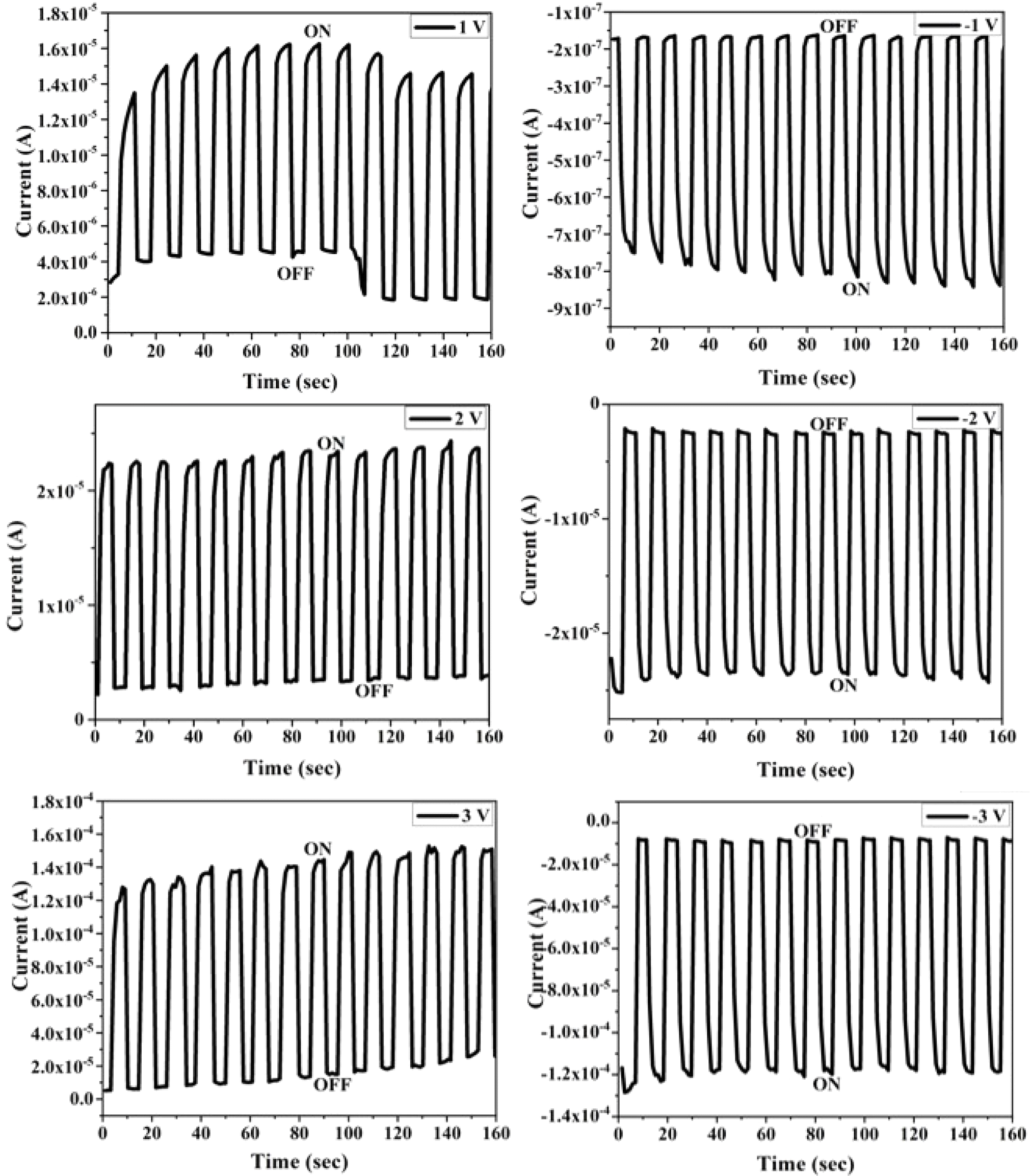 | ||
| Fig. 6 Bias voltage dependent relaxation response curves of the proposed MSM UVPD made of the Fe–SiC on aluminium layer. | ||
| V Bias (V) | I d (A) | I ph (A) | S (%) | G | t Res (s) | t Rec (s) |
|---|---|---|---|---|---|---|
| 1 | 1.94 × 10⁻⁵ | 23.2 × 10⁻⁶ | 555.36 | 6.55 | 6.55 | 6.55 |
| 2 | 1.06 × 10⁻⁵ | 31.47 × 10⁻⁵ | 1522.16 | 16.22 | 16.22 | 16.22 |
| 3 | 2.14 × 10⁻⁵ | 14.2 × 10⁻⁵ | 1239.62 | 13.39 | 13.39 | 13.39 |
| −1 | 3.94 × 10⁻⁶ | 61.8 × 10⁻⁵ | 278.85 | 28.87 | 28.87 | 28.87 |
| −2 | 1.17 × 10⁻⁵ | 280.7 × 10⁻⁶ | 7024.36 | 71.24 | 71.24 | 71.24 |
| −3 | 1.94 × 10⁻⁵ | 46.3 × 10⁻⁵ | 3857.26 | 39.57 | 39.57 | 39.57 |
Aluminium and its alloys have a wide range of applications in many fields owing to their excellent properties. Laser surface alloying has attracted growing interest in recent years and excellent coatings with high hardness, improved wear resistance and corrosion properties have been obtained. The approach proposed in this study for developing a laser-treated Fe–SiC alloyed aluminium layer achieved improved crystal phases and surface hardness of the alloyed surface with increase in the number of laser pulses up to 7 pulses. The MSM UVPD developed based on the alloyed material exhibited fast detection capacity as confirmed by the rapid rise and decay of peak current under ‘on and off’ lighting. The observed low leakage current of the photodetector indicates significant enhancement in the electrical properties of the aluminium. However, the technique was found to be ineffective beyond the 7 pulses, and the average microhardness dropped and remained almost the same as that of the aluminum base.
4. Conclusion
Laser-induced breakdown was successfully employed for surface alloying using a Q-switched Nd:YAG laser. The high plasma temperatures (>10000 K) and rapid quenching rates (5 × 10³ to 5 × 10⁶ K s−1) facilitated the formation of Al–Fe–Si, Si–Al, and Fe–Si alloyed composites on aluminum substrates pre-coated with Fe and SiC mixtures. XRD analysis confirmed the creation of ternary and binary phases, while SEM revealed significant microstructural changes, including porosities, wavy surfaces, and brittle regions caused by surface tension gradients and pressure effects. The hardness of the alloyed surface initially increased with up to 7 laser pulses, enhancing Fe–SiC phase formation, but plateaued with further irradiation. Additionally, photodetector properties were evaluated, with mean barrier heights of 0.76–0.84 eV and response/recovery times ranging from 0.21–1.81 s. These findings demonstrate the potential of laser-induced alloying to produce high-performance materials with tailored microstructures and enhanced properties.
Data availability
The data supporting this article have been included in the manuscript.Conflicts of interest
The authors declare that they have no conflict of interest.Acknowledgements
The authors gratefully acknowledge the financial support from Fallujah University and Iraq Ministry of Education.References
- S. Mohan and A. Mohan, Wear, friction and prevention of tribo-surfaces by coatings/nanocoatings, in Anti-Abrasive Nanocoatings, Elsevier, 2015, pp. 3–22 Search PubMed.
- A. Matthews and D. S. Rickerby, Advanced Surface Coatings: A Handbook of Surface Engineering, Springer, 1991 Search PubMed.
- C. Dawes, Surf. Eng., 1991, 7, 29 CrossRef CAS.
- A. Zhecheva, et al. , Surf. Coat. Technol., 2005, 200, 2192 CrossRef CAS.
- K. Holmberg and A. Matthews, Coatings Tribology: Properties, Mechanisms, Techniques and Applications in Surface Engineering, Elsevier, 2009 Search PubMed.
- F. Chen, X.-L. Wang and K.-M. Wang, Opt. Mater., 2007, 29, 1523 CrossRef CAS.
- J. Burnell-Gray and P. K. Datta, Surface Engineering Casebook: Solutions to Corrosion and Wear-Related Failures, Woodhead Publishing, 1996 Search PubMed.
- W. M. Steen, Laser Material Processing, Springer, 2010 Search PubMed.
- T. Sudarshan, Surface Modification Technologies: An Engineer's Guide, ed. M. Dekker, 1989 Search PubMed.
- C. Draper and C. Ewing, J. Mater. Sci., 1984, 19, 3815 CrossRef CAS.
- C. Draper and J. Poate, Int. Met. Rev., 1985, 30, 85 CAS.
- A. Basu, A. N. Samant, S. P. Harimkar, J. Dutta Majumdar, I. Manna and N. B. Dahotre, Surf. Coat. Technol., 2008, 202, 2623 CrossRef CAS.
- T. Welis, Surf. J., 1978, 9, 2 Search PubMed.
- F. Von Buch and B. Mordike, High-temperature properties of magnesium alloys, Magnesium—Alloys and Technology, Wiley, Hoboken, NJ, USA, 2004 Search PubMed.
- E. McCafferty, E. Shafrin and J. McKay, Surf. Technol., 1981, 14, 219 CrossRef CAS.
- A. Popoola, et al. , Int. J. Electrochem. Sci., 2016, 11, 126 CrossRef CAS.
- Y. Chi, et al. , Opt Laser. Eng., 2018, 100, 23 CrossRef.
- M. Quazi, et al. , Crit. Rev. Solid State Mater. Sci., 2016, 41, 106 CrossRef CAS.
- A. H. Ali, Diagnostic of Laser Plasma Using Optical Techniques, Universiti Teknologi Malaysia, 2004 Search PubMed.
- L. Mabhali, S. Pityana and N. Sacks, J. Laser Appl., 2010, 22, 121 CrossRef CAS.
- A. A. Naufal, et al. , Appl. Mech. Mater., 2013, 393, 9 Search PubMed.
- S. Banovic, et al. , Energy, 1999, 1, 1600 Search PubMed.
- H. R. Abd, et al. , Int. J. Electrochem. Sci., 2013, 8, 11461 CrossRef CAS.
- K. Bourenane, A. Keffous and G. Nezzal, Vacuum, 2007, 81, 663 CrossRef CAS.
- W. Zhang, et al. , Appl. Surf. Sci., 2010, 256, 4423 CrossRef CAS.
- A. M. Selman and Z. Hassan, Sens. Actuators, A, 2015, 221, 15 CrossRef CAS.
- Y. Takahashi, et al. , Jpn. J. Appl. Phys., 1994, 33, 6611 CrossRef CAS.
- A. A. Thahe, et al. , Opt. Quantum Electron., 2020, 52, 1 CrossRef.
- H. R. Abd, et al. , Int. J. Electrochem. Sci., 2013, 8, 11461 CrossRef CAS.
| This journal is © The Royal Society of Chemistry 2025 |