
 Open Access Article
 This Open Access Article is licensed under a Creative Commons Attribution-Non Commercial 3.0 Unported Licence
Recent advances and mechanism of plasmonic metal–semiconductor photocatalysis
Ting Kong *a,
Aizhen Liaoa,
Yonggang Xua,
Xiaoshuang Qiaoa,
Hanlu Zhanga,
Linji Zhanga and
Chengyun Zhangb
*a,
Aizhen Liaoa,
Yonggang Xua,
Xiaoshuang Qiaoa,
Hanlu Zhanga,
Linji Zhanga and
Chengyun Zhangb
aSchool of Science, Xi'an University of Posts & Telecommunications, Xi'an 710121, China. E-mail: kongting0302@xupt.edu.cn; azliao@xiyou.edu.cn; ygxu@xupt.edu.cn; qiaoxs@xupt.edu.cn; zhanghl@xupt.edu.cn; zhanglinji@xupt.edu.cn
bSchool of Electronic Engineering, Xi'an University of Posts & Telecommunications, Xi'an 710121, China. E-mail: cyzhang@xupt.edu.cn
First published on 28th May 2024
Abstract
Benefiting from the unique surface plasmon properties, plasmonic metal nanoparticles can convert light energy into chemical energy, which is considered as a potential technique for enhancing plasmon-induced semiconductor photocatalytic reactions. Due to the shortcomings of large bandgap and high carrier recombination rate of semiconductors, their applications are limited in the field of sustainable and clean energy sources. Different forms of plasmonic nanoparticles have been reported to improve the photocatalytic reactions of adjacent semiconductors, such as water splitting, carbon dioxide reduction, and organic pollutant degradation. Although there are various reports on plasmonic metal–semiconductor photocatalysis, the related mechanism and frontier progress still need to be further explored. This review provides a brief explanation of the four main mechanisms of plasmonic metal–semiconductor photocatalysis, namely, (i) enhanced local electromagnetic field, (ii) light scattering, (iii) plasmon-induced hot carrier injection and (iv) plasmon-induced resonance energy transfer; some related typical frontier applications are also discussed. The study on the mechanism of plasmonic semiconductor complexes will be favourable to develop a new high-performance semiconductor photocatalysis technology.
1. Introduction
With the increasing shortage of global environmental resources, semiconductor photocatalysis has become a very promising technology and has attracted considerable attention of researchers.1–3 Owing to the outstanding physical and chemical performances, semiconductor catalysts can realize the effective conversion of solar energy into chemical energy, and have been widely used in environmental governance, water purification, carbon dioxide reduction and other industrial applications.4–6 When the light energy is larger than the band gap of the semiconductor, electron–hole (e−/h+) pairs will be generated on a femtosecond time scale, which will participate in redox reactions.7 However, the application of semiconductor materials has been greatly limited by defects of the high recombination rate of e−/h+ pairs, large band gap and low utilization of visible light.8 Recent progress has focused on improving the light absorption efficiency of semiconductor materials, inhibiting the recombination of photogenerated carriers, and enhancing the activity of catalysts.9–11 Therefore, designing a novel and efficient semiconductor photocatalyst is important for improving the energy conversion efficiency.Different strategies such as vacancies, doping, surface reconstruction, heterogeneous construction, and noble metal modification have been explored to regulate the performance of semiconductor photocatalysts.12–14 Among them, the use of noble metal nanoparticles (NPs) (such as Au, Ag, and Cu) is a promising approach to drive a chemical reaction due to their unique feature of localized surface plasmon resonance (LSPR), and the plasmons are collective oscillations of free electrons on a metal surface driven by the incident light at or near the oscillation frequency.15–18 During the decay of LSPR, the energies stored in the local electromagnetic field can be reradiated via scattering and the oscillations can dephase into hot electron generation, resulting in the absorption of light by plasmonic NPs.19,20 Owing to the great light harvesting and light scattering ability, plasmonic metals provide an efficient way to enhance the photoconversion performance by transferring solar energy to adjacent semiconductors.21,22 For plasmon-semiconductor composite materials, plasmonic metal NPs can inhibit charge carrier recombination by plasmon-induced hot electron injection or plasmon-induced resonance energy transfer.23 By transferring plasmonic energy or hot electrons in a direct/indirect way to adjacent semiconductors, the utilization of visible light and photocatalytic performance of semiconductors are improved.24
Numerous plasmonic metal–semiconductor composites have been devoted to control plasmon-enhanced photocatalysis, while few studies have focused on generalizing the mechanism. In this perspective, recent progress in plasmonic metal–semiconductor photocatalysis is simply discussed with emphasis on the main four mechanisms: (i) enhanced local electromagnetic field, (ii) light scattering, (iii) plasmon-induced hot carrier injection and (iv) plasmon-induced resonance energy transfer. In addition, we summarize the development of plasmonic semiconductors for photocatalysis and their prospects, hoping to provide effective theoretical guidance and approaches for the design and application of new plasmonic metal–semiconductor photocatalysts.
2. Plasmonic semiconductor photocatalysts
Since the concept of ‘plasmonic photocatalysts’ was first proposed by Awazu et al. in 2008, various plasmonic metal/semiconductor composites were employed to achieve plasmon-enhanced semiconductor photocatalysis, which have been widely applied in the fields of energy conversion and environmental governance.25 Due to their unique LSPR property, the noble metal nanostructures can increase the light absorption ability and reduce the electron–hole recombination rate by trapping photogenerated electrons transferred from the semiconductor photocatalyst, thus promoting the reaction efficiency of photocatalysis. Au and Ag nanostructures are often used as supports for plasmon-enhanced semiconductor photocatalysis due to their excellent electromagnetic properties and visible light response. Razzari et al. achieved enhanced photocatalytic activity of Au–TiO2 nanohybrids for water splitting by controlling the absorption and local electric field based on whispering gallery mode resonances.26 Zhou et al. designed Ag@TiO2 nanocatalysts used for single-molecule imaging, in which the catalytic activities and hot electrons generated by Ag core are affected by the TiO2 shell thickness.27 Moreover, other plasmonic metal NPs such as Pt, Cu, Al, Bi, and Co are used to achieve high photocatalytic efficiency, and have been reported in many works. For instance, Jia et al. prepared Pt/γ-Al2O3 plasmonic catalysts to effectively degrade volatile organic compounds under sunlight irradiation based on the plasmonic photothermal effect of Pt NPs.28 Zeng et al. realized broad-spectrum absorption under near-infrared irradiation by using Cu NPs hybridized with carbon quantum dots, which possess a high catalytic efficiency for H2 evolution due to the SPR effect of Cu NPs.29 In addition, bimetallic nanostructures such as Au/Ag, Pt/Cu, and Au/Cu are developed as potential candidates for plasmon-induced semiconductor photocatalysis, which delivers enhanced catalytic performance not possible with their individual components under certain conditions.30–32The typical semiconductor material of TiO2 as a green technology was first reported by Fujishima et al. in 1972 and has been widely used in the photocatalysis field.33 However, the bandgap of TiO2 is 3.2 eV, which only absorbs ultraviolet light and limits its applications. Then, various semiconductor materials have been designed to facilitate the application of photocatalysis in the field of environmental treatment and energy conversion, including semiconductor oxide photocatalysts such as ZnO, Cu2O, WO3, and Fe2O3, perovskite structured ABO3 materials such as BiTiO3, SrTiO3, NaTaO3, and PrFeO3, and novel bismuth photocatalysts such as BiOX (X = F, Cl, Br, and I), Bi2O3, Bi2MO6 (M = Cr, Mo and W), and BiVO4.34–36 In addition, since the emergence of monolayer graphenes, two-dimensional (2D) nanomaterials and layered nanomaterials have been designed to promote the development of photocatalysis due to their thickness-dependent physical and chemical properties.37 Although plasmonic semiconductor photocatalysts have made remarkable achievements in energy conversion, their structural design optimization, mechanism explanation and photocatalytic efficiency still need to be improved.
3. Mechanism of plasmonic metal–semiconductor photocatalysis
With the development of plasmonic photocatalysts, LSPR-enhanced photocatalysis has become a green technology to solve the problems of energy shortage and environmental pollution by using solar energy, which has attracted extensive attention in recent decades. LSPR decay can achieve significant electromagnetic field enhancement in the nanoscale “hot spot” area around the plasmonic metal NP surface, which is called near-field enhancement, leading to strong light absorption and enhanced carrier generation. For plasmonic metal semiconductor composites, four possible mechanisms of plasmon-enhanced semiconductor photocatalysis are proposed and briefly discussed below (Fig. 1).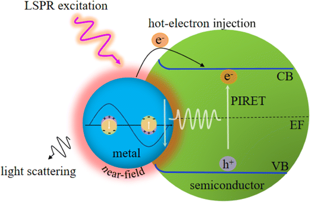 | ||
| Fig. 1 Mechanism diagram for plasmonic metal–semiconductor photocatalysis. | ||
3.1. Enhanced local electromagnetic field
For metal–semiconductor composite nanostructures, the localized field enhancement effect caused by surface plasmon decay of metal nanostructures can improve the light absorption of adjacent semiconductor materials. Due to the strong localized effect of field enhancement, the spatial distribution of photogenerated electron–hole pairs inside the semiconductor material can be regulated, and the distance of charge diffusion to the surface is shortened, thereby suppressing the carrier recombination and improving the charge separation efficiency.Liu et al. reported that the photocatalytic conversion rate of hydrogen evolution using Au nanochains was significantly higher than that of conventional isolated Au NPs due to the enhanced local electromagnetic field effect (Fig. 2).38 The short distance between Zn0.67Cd0.33S semiconductors and plasmonic Au-nanochain is favourable for the transfer of plasmonic energy from metal to semiconductor. The strongly coupled Au-chain exhibits an intense local electromagnetic field, which enhances the charge carrier's formation rate and lifetime, thus improving the photocatalytic activity of semiconductors. Zou et al. achieved plasmon-enhanced photocatalytic reduction of CO2 using Au@TiO2 yolk–shell hollow spheres based on local field enhancement effect. Au nanostructures not only enhance the generation and separation efficiency of charge carriers in TiO2 shells, but also promote the generation of high-grade carbon species, thus contributing to the improvement of photocatalytic performance.39
 | ||
| Fig. 2 Simulated near-field distributions of isolated Au NPs and Au nanochips with five coupled Au NPs using FDTD.38 Reproduced from ref. 38 with permission from Springer Nature, copyright [2019]. | ||
3.2. Light scattering
Upon irradiation, the decay of surface plasmon resonance radiation induces the generation of photons, which are scattered into the adjacent semiconductor material with extremely large light absorption and light scattering cross-sections. The light trapping effect caused by plasmonic light scattering can increase the optical path in semiconductor materials, thereby enhancing the light-harvesting ability and generation rate of charge carriers.40 Furthermore, plasmonic light absorption makes the metal nanostructure itself an efficient light-trapping centre. If the light energy captured by the plasmon can be effectively utilized, the energy conversion efficiency can be greatly improved.Liu et al. designed a novel Au/Cu2O/Pt photoelectrode to achieve highly efficient photoelectrochemical water splitting due to enhanced light harvesting and photoinduced charge separation.42 Under light irradiation, the plasmonic hot electrons generated by the Au nanolayer were transferred to the CB of Cu2O and increased the light-harvesting ability. A Schottky barrier was established between Cu2O and the Pt layer, which lead to the electron transfer from Cu2O to Pt. In addition, the rearrangement of the energy band of Cu2O and Pt resulted in a reduction in the potential barrier and promoted the separation of electron–hole pairs, thereby enhancing the photocatalytic performance. The results of this work show that the enhanced light-harvesting ability is a synergistic effect of the SPR effect of Au and the photoinduced charge transfer effect of Pt, which provides a promising strategy for developing high-performance plasmonic and semiconductor cocatalysts. Wang et al. realized highly efficient photocatalytic reduction of nitrate into N2 by constructing a novel core–shell Ag/SiO2@cTiO2 composite.43 Due to the strong light-scattering effect at the core–shell interface and the SPR effect of Ag NPs, the light-harvesting efficiency of the semiconductor is enhanced. Meanwhile, the separation efficiency of photogenerated electron–hole pairs is also enhanced by charge transfer from the TiO2 shell to Ag NPs, which promotes the enhancement of photocatalytic performance and the stability of Ag/SiO2@cTiO2 composites. Zhang et al. designed a novel Ag@Si2O@TiO2–Au plasmonic semiconductor photocatalyst system, which can achieve a higher photocatalytic activity for H2 production due to the strong plasmonic light scattering and field enhancement effect (Fig. 3).41 Ag NPs served as a plasmonic resonator not only to increase the optical path of photocatalytic reaction via SPR scattering, but also to strengthen the local electric field of the TiO2–Au interface by Ag–Au coupling, leading to enhanced light absorption ability and separation efficiency of charge carriers, thereby boosting the catalytic activity of Ag@Si2O@TiO2–Au nanohybrids.
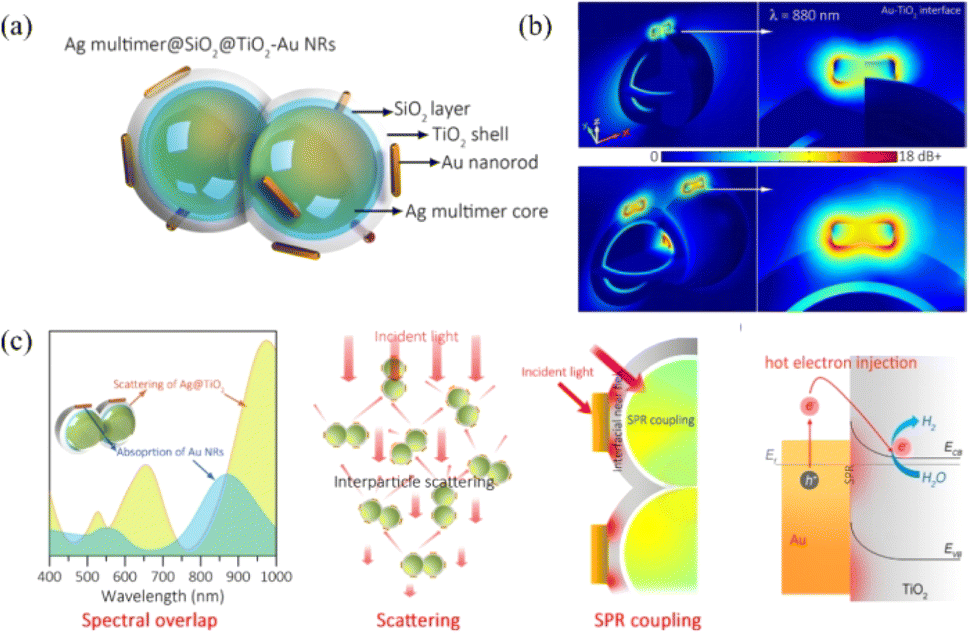 | ||
| Fig. 3 Enhancement of scattering and near-field distribution of TiO2–Au nanohybrids using a silver resonator for plasmonic photocatalysis: (a) schematic of the Ag multimer@Si2O@TiO2–Au nanostructure; (b) simulated electric field enhancement distribution of Ag mono@TiO2–Au and Ag multi@TiO2–Au nanohybrids; (c) schematic of plasmonic Ag NP-enhanced light harvesting, including the spectral overlap, scattering, SPR coupling and hot electron injection.41 Reproduced from ref. 41 with permission from the American Chemical Society, copyright [2021]. | ||
3.3. Plasmon-induced hot carrier injection
The hot carriers (electrons or holes) are generated via radiative photon emission or nonradiative relaxation during the LSPR decay process, which play a dominant role in driving photochemical transformation.44,45 For the photocatalytic mechanism of the plasmonic/semiconductor composite structure, there are two possible pathways for the LSPR-induced hot electron effect: one is direct hot electron transfer, and the other is indirect hot electron transfer (tunnelling effect) (Fig. 4).10 The hot electrons with higher energy under illumination are injected into the conduction band (CB) of the adjacent semiconductor, and they can activate specific chemical bonds in reactants and alter reaction pathways to regulate product selectivity, thereby enhancing the photocatalytic efficiency.46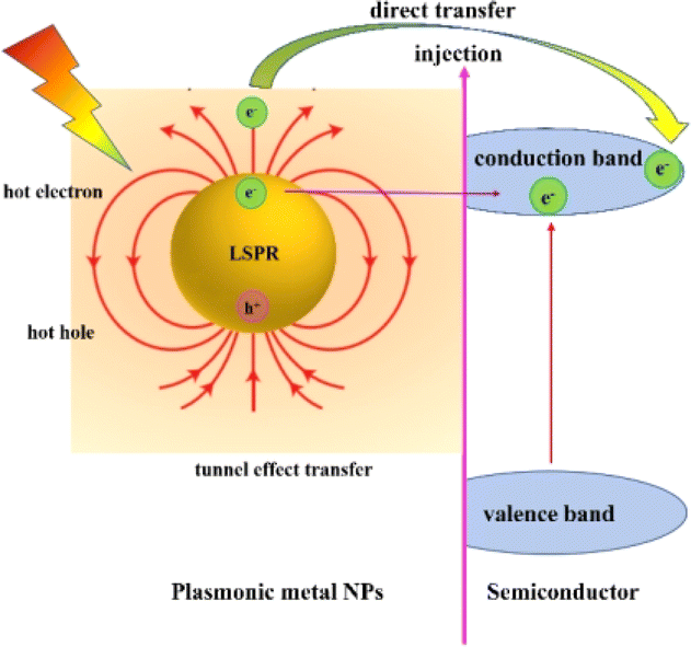 | ||
| Fig. 4 Schematic of the hot electron injection mechanism for plasmonic semiconductors. | ||
In general, the indirect hot electron transfer process is a multi-step process with a low efficiency compared to the direct hot electron transfer process, which is a one-step transfer process in metal/semiconductor composite systems. The contact between the metal and the semiconductor usually forms the Schottky barrier. Metals and other plasmons excite intra- or inter-band transitions via electron–electron interaction to form hot electrons. When the energy of hot electrons is greater than the Schottky barrier, they can be injected into the semiconductor across the barrier. In addition to crossing the Schottky barrier, hot electrons can be injected into the semiconductor by the tunnelling transfer effect.
Chen et al. investigated the shell thickness dependence of the plasmon-induced hot electron injection process by designing an Au@CdS core–shell nanocrystal for photocatalysis (Fig. 5).47 The results indicated that the hot electron injection efficiency first increases and then decreases after a critical point around 8–10 nm with the increase in CdS shell thickness, which was mainly determined by hot-electron energy distribution of the Au core and the Schottky potential between the Au core and the CdS shell. This work provides a new approach for optimizing the photocatalytic performance of plasmonic semiconductor systems. Choudhury et al. discussed the photocatalytic performance of binary hybrids of Ag–TiO2 and Au–TiO2 and ternary plasmonic semiconductor heterostructures of Ag–TiO2–CN and Au–TiO2–CN in the degradation of RhB and phenol, and clarified the mechanism for enhanced photocatalysis.48 For binary hybrids, the enhanced photocatalytic activity was attributed to the hot electron injection (direct or indirect) from Ag (or Au) to TiO2 and localized electromagnetic field enhancement effect near the metal–semiconductor interface. As regards the ternary hybrids, it is evidenced that the enhanced photocatalytic activity is caused by hot electron injection either via quantum tunnelling or intermediate states with assistance of interfacial charge transfer from TiO2 to C3N4, which can reduce the recombination rate of carriers and improve the ability of photodegradation of pollutants. In addition, the Ti3+ states in the TiO2 surface can increase the possibility of quantum tunnelling effect of the plasmonic electrons and facilitate direct transfer of hot electrons from the metal to the semiconductor, thereby contributing to enhanced photocatalytic efficiency.
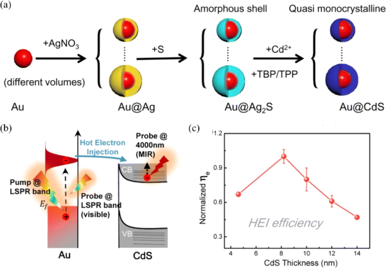 | ||
| Fig. 5 Plasmon-induced hot electron injection in the Au@CdS core–shell nanocrystal: (a) schematic of the preparation process of the Au@CdS core–shell nanocrystal; (b) schematic of the hot electron injection process between Au and CdS under pump LSPR band excitation; and (c) hot electron injection efficiency as a function of CdS thickness.47 Reproduced from ref. 47 with permission from the American Chemical Society, copyright [2021]. | ||
Besides the plasmon-induced hot carrier effect, the coupling of phonons and electrons exists at the interface between the metal and the semiconductor hybrid system, which can be affected by controlling the temperature. Jacinto et al. studied the effect of phonons on plasmon-induced hot electron generation and charge transfer for Au/TiO2 and Au/ZrO2 hybrid systems under different operating temperatures.49 The results indicated an increase in the number of hot carriers transferred from the plasmonic Au material to the TiO2 semiconductor conduction band with the increase in temperature by transient ultrafast infrared spectroscopy technology. The increase in hot carrier injection is attributed to the phonon-enhanced hot carrier generation (phonons transfer momentum to electrons) or phonon-assisted hot carrier transfer across the Au/TiO2 interface barrier (phonons transfer energy to hot carriers). As the height of the Schottky barrier increases with the increase in temperature, the electron injection efficiency is reduced. Therefore, due to phonon-assisted hot electron generation, the plasmon-induced hot carrier injection of the Au NP/TiO2 hybrid system increases with the increase in temperature. This work provides a new approach for the application of plasmonic devices.
3.4. Plasmon-induced resonance energy transfer
Plasmon-induced resonance energy transfer (PIRET) refers to the transfer of trapped energy by surface plasmons via dipole–dipole interactions to adjacent semiconductors.50,51 PIRET is a non-radiative relaxation channel of surface plasmons, which can be observed on strong coupling between plasmons and excitons.52 The Förster resonance energy transfer (FRET) effect is a similar process commonly used to describe the energy transfer between two chromophores (fluorescent dye molecules or semiconductor quantum dots) in which the donor excited state energy can be transferred to the receptor.53 However, FRET is a weakly coupled and incoherent process that occurs after the thermal relaxation of the excited state. The PIRET in the plasmon-semiconductor hybrid system is an ultrafast coherent process, which can achieve a higher energy conversion efficiency in photocatalytic applications.54Wu et al. elaborated the mechanism of PIRET by employing the Au@SiO2@Cu2O core–shell NPs and distinguished the theory of PIRET from FRET.54 The energy transfer between plasmon and semiconductor depends on the dipole moments. Under dipole–dipole coupling, if the plasmon is excited, which the energy is transferred to the Cu2O semiconductor by PIRET, conversely, the energy is transferred from the Cu2O semiconductor to the plasmon by FRET. In addition, the PIRET efficiency can be controlled by spatial distance and spectral overlap between the plasmonic Au nanostructure and the Cu2O semiconductor. The experimental results indicate that a thin dielectric layer of SiO2 can inhibit electron transfer and provide the largest PIRET enhancement due to the LSPR effect of Au and the PIRET effect. Moreover, PIRET is an ultrafast and coherent process that occurs before the thermal relaxation of the plasmon, and it can effectively promote light absorption by utilizing the energy near and below the band gap of semiconductors.
In addition, Wu et al. designed metal@TiO2 core–shell NPs in order to control the PIRET and HEI process by changing the spectral overlap and introducing SiO2 layer (Fig. 6).23 The relative increase in carrier density for PIRET depends mainly on the spectral overlap between plasmons and semiconductors and HEI mainly depends on plasmon absorption. The extinction spectra showed that the spectral overlap for Ag@TiO2 was significantly enhanced compared to that of pure TiO2, while there is no spectral overlap for plasmonic Au NPs with the interband transitions dominated below the wavelength of 500 nm (Fig. 6b). Both the PIRET and HEI processes are favorable to enhance the photoconvention for metal/TiO2 semiconductor systems (Fig. 6c). Moreover, the transient absorption spectroscopy was performed to study plasmonic the enhancement mechanism (Fig. 6d). The results demonstrated that both the PIRET and HEI processes occurred for the Ag@TiO2 system, while for Au@TiO2, only HEI transferred from Au to TiO2. Due to the spectral overlap, the PIRET can occur for Ag@SiO2@TiO2 NPs. There is no PIRET or HEI occurring for Au@SiO2@TiO2 NPs. This work contributes to better understand the mechanism of plasmon-enhanced light conversion.
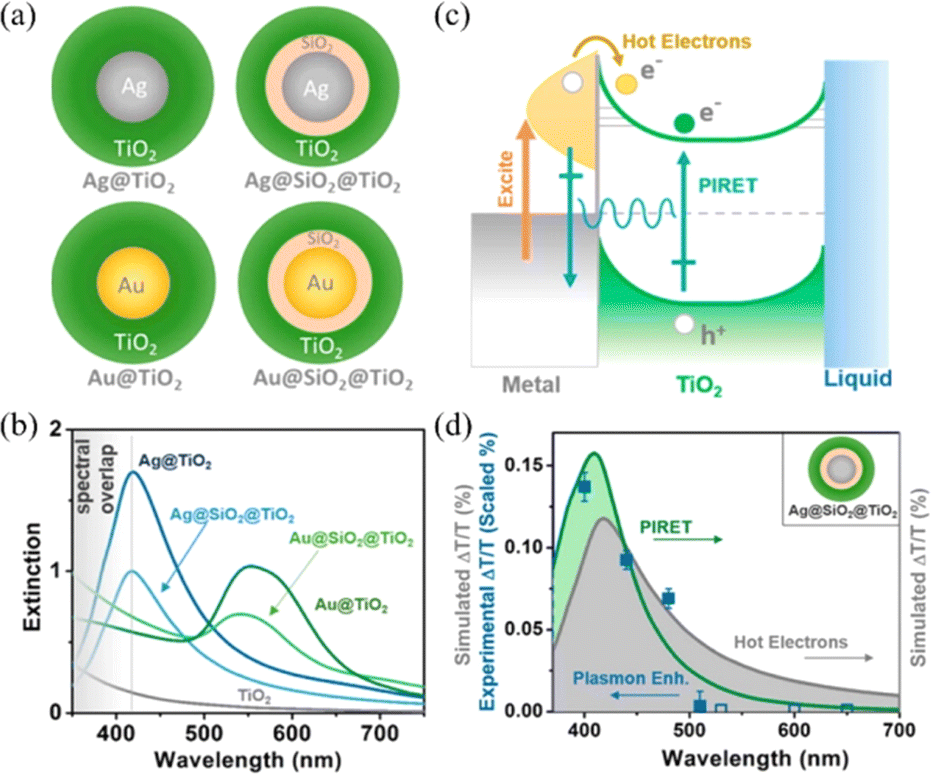 | ||
| Fig. 6 Controlling PIRET and HEI for metal@TiO2 core–shell NPs: (a) schematic of the metal@ TiO2 core–shell NPs; (b) extinction spectra of the metal@TiO2 NPs; (c) schematic of the PIRET and HEI mechanism of the metal@TiO2 system; and (d) experimental and simulated change of transmission for Ag@SiO2@TiO2 as a function of wavelength.23 Reproduced from ref. 23 with permission from the American Chemical Society, copyright [2015]. | ||
4. Applications
Benefiting from the LSPR effect of plasmonic NPs, the absorption cross-section of semiconductors, and light absorption range and electron–hole charge separation rate of semiconductor can be effectively improved, thus expanding the applications of plasmonic semiconductors in the field of photocatalysis. In this section, we discuss the recent progress in plasmon-enhanced semiconductor photocatalysis for various applications including energy conversion and environmental remediation. The various applications of typical plasmonic metal–semiconductor photocatalysts are listed in Table 1.| Plasmonic metal-semiconductors | Photocatalytic applications | Published year | Reference |
|---|---|---|---|
| Au–TiO2 | Photocatalytically oxidize ethanol and methanol; photovoltaic fuel cell | 2005 | 55 |
| Ag/SiO2–TiO2 | Decomposition of MB | 2008 | 56 |
| Au@CeO2 | Oxidation of benzyl alcohol to benzaldehyde | 2014 | 57 |
| Au/ZnO | MO dye degradation | 2016 | 58 |
| Au/Cu2O/Pt | Water splitting | 2018 | 42 |
| Au chain@Zn0.67Cd0.33S | Photocatalytic hydrogen evolution | 2019 | 38 |
| Cu-doped ZnO–CuO | Photo-decontamination of textile effluents | 2020 | 59 |
| Mg/MgO | SF6 environmental remediation | 2020 | 60 |
| Bi/α-MnS/Bi2MoO6 | CO2 reduction | 2021 | 5 |
| Ag/SiO2@cTiO2 | Photocatalytic reduction of nitrate | 2021 | 43 |
| Ag/BiFeO3 fibrous | Photoelectrochemical energy conversion | 2021 | 61 |
| SiO2–Au–Pt | Degradation of MB | 2021 | 62 |
| Ag/BiVO4 | Photodegradation of RhB | 2022 | 63 |
| Au NBP@Cu2O | Treatment of breast cancer | 2023 | 64 |
| Bi/TiO2 | CO2 reduction | 2024 | 65 |
4.1. Energy application
The photocatalytic water-splitting process based on plasmonic metal–semiconductors enables obtaining an effective, clean, and environmentally friendly renewable energy source, which has been widely studied by many researchers in recent years with the aim of improving photocatalytic hydrogen production performance.66 Liu et al. realized plasmon-enhanced photocatalytic water splitting with a Au NPs/TiO2 composite under visible light irradiation (Fig. 7).67 The results show that the photocurrent of TiO2 can be enhanced by 66 times with plasmonic Au NPs at 633 nm excitation, indicating that the photocatalytic water splitting ability is significantly enhanced due to the local field enhancement effect. Yoon et al. provided an approach for photocatalytic water splitting by designing a Ag NP–impregnated BiVO4 nanocomposite (Fig. 8).68 The photoelectrochemical measurement and the simulation results show that the catalytic performance of Ag/BiVO4 nanocomposites is significantly higher than that of original materials, which is attributed to the increased carrier generation and charge separation efficiency caused by the LSPR effect.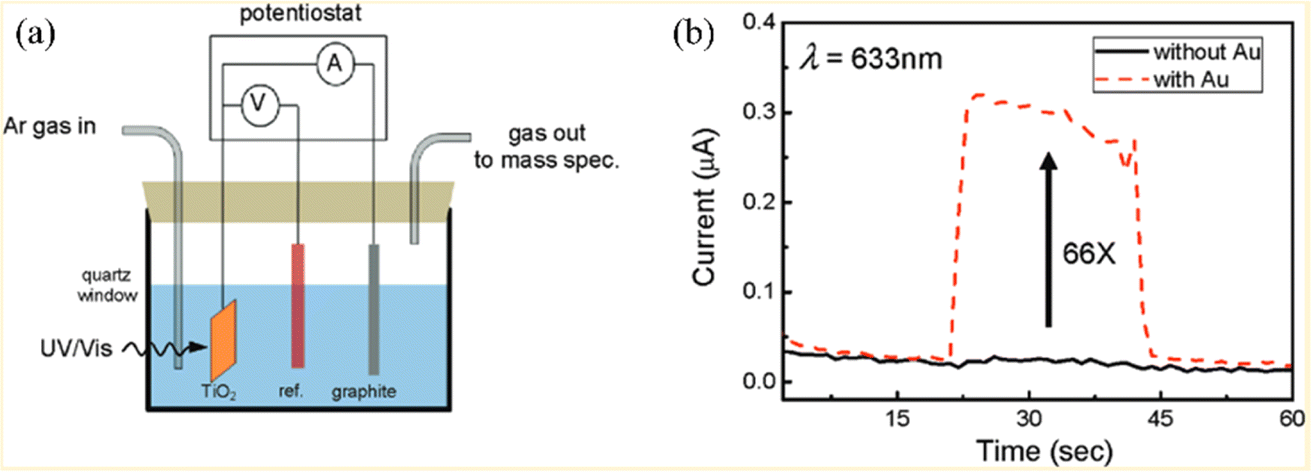 | ||
| Fig. 7 Applications of plasmon-enhanced photocatalytic water splitting with Au NP/TiO2 composites: (a) schematic of the TiO2 photocatalytic water-splitting experimental device and (b) photocurrent of TiO2 with and without Au NPs under 633 nm excitation.67 Reproduced from ref. 67 with permission from the American Chemical Society, copyright [2011]. | ||
 | ||
| Fig. 8 Applications of plasmon-enhanced photocatalytic water splitting with a Ag NP-impregnated BiVO4 composite: (a) absorption enhancement of BiVO4 with and without Ag NPs; (b) simulated light absorption distribution of BiVO4 with a Ag NP; and (c) current density as a function of the potential of BiVO4 with and without Ag NPs.68 Reproduced from ref. 68 with permission from the American Chemical Society, copyright [2018]. | ||
Plasmon-driven semiconductor photocatalytic carbon dioxide (CO2) reduction to hydrocarbon fuels has attracted widespread attention as a promising strategy for producing solar fuels and reducing greenhouse gases, which needs the design of highly efficient photocatalysts that can be boosted by the broad spectrum of wavelengths of sunlight.39 Long et al. reported the broadband CO2 reduction reaction with water to hydrocarbons by plasmonic Au rod@CuPd2 nanostructures, which provided a new strategy for energy conversion with near-infrared photons (Fig. 9).69 In this work, a co-catalyst of Au nanorods with CuPd2 shells was designed to realize an enhanced plasmon-driven photocatalytic efficiency. The yield rate of CH4 is 0.55 mmol g−1 h−1 under full-spectrum light with 100% selectivity for hydrocarbons and the apparent quantum efficiency (AQE) for Au rod@CuPd2 is 0.38% under 800 nm light irradiation (Fig. 9c and d). The X-ray photoelectron spectroscopy and theoretical calculation results show that the local electric field and electron transfer together promote the CO2 reduction reaction by effectively utilizing low-energy near-infrared light. Li et al. achieved plasmon-enhanced photocatalytic CO2 reduction efficiency for ammoniated α-MnS/Bi2MoO6 S-scheme heterostructures by the SPR effect of plasmonic Bi, which provide a novel insight into the field of plasmonic metal–semiconductor photocatalysis for energy conversion.5
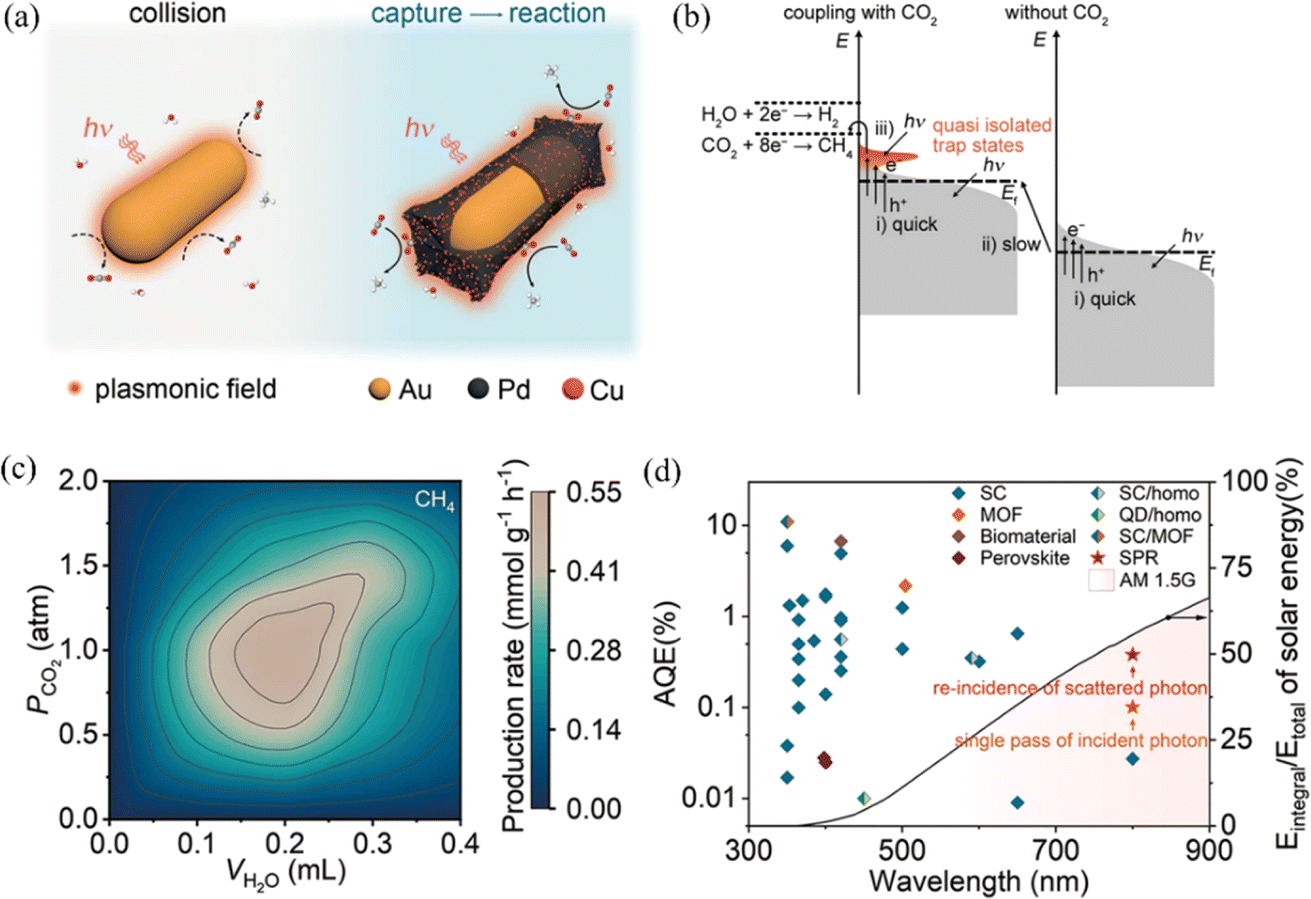 | ||
| Fig. 9 Applications of plasmon-induced CO2 reduction with Au rod@CuPd2: (a) schematic of the plasmon-induced CO2 reduction for pure Au rods (left) and Au@CuPd2 (right); (b) schematic of the mechanism of plasmon-induced CO2 reduction reaction, (c) production rate of CH4 under different CO2 pressures and H2O volumes and (d) AQE of Au rod@CuPd2.69 Reproduced from ref. 69 with permission from Springer Nature, copyright [2023]. | ||
Ammonia as a carbon-free solar energy storage material can be manufactured from N2 or water. Plasmon-induced photocatalytic nitrogen fixation is considered as a promising green artificial technology for green ammonia production.70–72 Fang et al. achieved high-performance nitrogen fixation driven by plasmonic Au/Ru electrocatalysts.73 Due to the inertness of plasmonic AuNPs, Ru acts as a bridge to promote the effective utilization of hot electrons by transferring directly from Au to N2, thereby enhancing the plasmon-induced N2 fixation rate. Moreover, Zhang et al. utilized porous CuFe to achieve the application of plasmonic Cu photocatalysts in N2 photofixation.74
4.2. Environmental application
Besides, plasmonic metal–semiconductor photocatalysis has achieved great progress in other applications such as environmental governance, and cancer treatment.75–77 Haghighi et al. achieved high-performance MB photodegradation by designing an ultra-porous Cu plasmon-induced CuZnO–CuO heterojunction.78 The experiment results indicated that when the fuel ratio increases from 0.5 to 2, the degradation ability of the dye was enhanced significantly due to the increase in charge carrier separation and SPR mechanism of Cu NPs. Sun et al. designed a plasmonic Z-scheme Cu2O/Bi/Bi2MoO6 heterojunction, which exhibits an excellent photocatalytic activity in the degradation of sulfadiazine and Ni(II) due to the SPR effect.79 Gutiérrez et al. first designed a plasmonic Mg/MgO NP platform with controllable LSPR effect, which presents high-performance photocatalytic properties for environmental remediation by degrading SF6 into non-toxic products of MgF2 and MgSO4.60 Chang et al. demonstrated that Au NBP@Cu2O nanozymes can effectively treat breast cancer under a near-infrared II window due to the plasmon-enhanced catalytic activity.645. Conclusions
Plasmon-enhanced photocatalysis has been a hot topic in recent years due to its unique surface plasmon properties. In this review, the main mechanism of plasmonic metal–semiconductor photocatalysis and its recent progress were briefly discussed. As for the plasmonic semiconductor composites, the localized field enhancement effect caused by the LSPR decay of metal nanostructures can improve the light absorption of adjacent semiconductor materials. The strong plasmonic light-harvesting and light-scattering ability makes the metal nanostructure itself become an efficient light-trapping centre, which plays a significant role in broadening the absorption wavelength range and improving the photocatalytic activity of semiconductor photocatalysts. The light energy stored in plasmonic metal NPs can be transferred to adjacent semiconductor materials that can maximize solar energy conversion. Moreover, plasmonic metal nanostructures can improve the photocatalytic performance of semiconductors by enlarging the light absorption region or enhancing the separation efficiency of electron–hole pairs by plasmon-induced hot electron injection or plasmon-induced resonance energy transfer.Although great progress has been made in plasmonic metal–semiconductor photocatalysis, the mechanism and other related issues need further systematic and in-depth study. For example, (i) designing new plasmonic nanomaterials: in traditional plasmonic metal–semiconductor photocatalysis systems, the plasmonic materials are usually noble metals such as Au and Ag, but they have limitations such as high cost, instability, and low utilization of visible light. Therefore, it is crucial to find new plasmonic materials that are economic and stable with low loss to achieve enhanced photocatalytic performance. (ii) Charge/energy transfer mechanism at the metal/semiconductor interface: it is well known that the mechanisms of plasmon-induced hot electron transfer and energy transfer are of great significance to explain the mechanism of plasmon-enhanced semiconductor photocatalysis. However, thus far, this interpretation is not very clear and is based on indirect proofs. Therefore, new ideas and technologies for directly characterizing the separation of electron–hole pairs and energy transfer between plasmons and semiconductors are still facing great challenges. (iii) Explore other synergy mechanism for plasmonic metal–semiconductor photocatalysis: based on the surface plasmon effect, not only the near-field enhancement, far-field scattering, charge transfer and energy transfer effects, but also the interaction of electrons and phonons and the photothermal effect will enhance the plasmonic metal–semiconductor photocatalysis. The synergy between them, as well as new mechanisms and insights, needs further experimental and theoretical exploration and discussion. (iv) Extensive research is required for plasmonic metal–semiconductor systems in order to expand the industrial application and commercial value with low cost, high stability and catalytic efficiency. It is believed that solving the above-mentioned problems will provide a new way for the development and application of plasmonic metal–semiconductor photocatalysis.
Author contributions
T. K. wrote and prepared the manuscript for submission; A. L. and Y. X. were involved in literature search and study design. X. Q., H. Z. and L. Z. contributed to the data analysis and discussion of the contents. C. Z. reviewed and supervised the manuscript. All authors have read and agreed to the published version of the manuscript.Conflicts of interest
There are no conflicts to declare.Acknowledgements
This work was supported by the National Natural Science Foundation of China (Grant 12204376, 12104366 and 22005243); Shaanxi Provincial Natural Science Foundation (Grant 2021JQ-700 and 2021JQ-699); Scientific Research Program Funded by Shaanxi Provincial Education Department (Program No. 20JK0905).References
- M. M. Abouelela, G. Kawamura and A. Matsuda, J. Cleaner Prod., 2021, 294, 126200 CrossRef CAS
.
- B. Liu, H. Wu and I. P. Parkin, ACS Omega, 2020, 5, 14847–14856 CrossRef CAS PubMed
- X. Sun, H. Huang, Q. Zhao, T. Ma and L. Wang, Adv. Funct. Mater., 2020, 30, 1910005 CrossRef CAS
- H. Wang, X. Li, X. Zhao, C. Li, X. Song, P. Zhang, P. Huo and X. Li, Chin. J. Catal., 2022, 43, 178–214 CrossRef CAS
- L. Liu, K. Dai, J. Zhang and L. Li, J. Colloid Interface Sci., 2021, 604, 844–855 CrossRef CAS PubMed
- M. Khademalrasool, M. Farbod and M. D. Talebzadeh, Adv. Powder Technol., 2021, 32, 1844–1857 CrossRef CAS
- J. Schneider, M. Matsuoka, M. Takeuchi, J. Zhang, Y. Horiuchi, M. Anpo and D. W. Bahnemann, Chem. Rev., 2014, 114, 9919–9986 CrossRef CAS PubMed
- T. Kong, X. Wei, G. Zhu and Y. Huang, J. Mater. Sci., 2017, 53, 708–715 CrossRef
- S. Li, P. Miao, Y. Zhang, J. Wu, B. Zhang, Y. Du, X. Han, J. Sun and P. Xu, Adv. Mater., 2021, 33, e2000086 CrossRef PubMed
- P. Jiménez-Calvo, V. Caps and V. Keller, Renewable Sustainable Energy Rev., 2021, 149, 111095 CrossRef
- D. Liu and C. Xue, Adv. Mater., 2021, 33, 2005738 CrossRef CAS
- T. Kong, X. Wei, G. Zhu and Y. Huang, Chin. J. Phys., 2017, 55, 331–341 CrossRef CAS
- T. Kong, X. Wei, G. Zhu and Y. Huang, J. Mater. Sci., 2017, 52, 5686–5695 CrossRef CAS
- Y. Li, M. Wen, Y. Wang, G. Tian, C. Wang and J. Zhao, Angew. Chem., Int. Ed., 2021, 60, 910–916 CrossRef CAS
- T. Kong, C. Zhang, X. Gan, F. Xiao, J. Li, Z. Fu, Z. Zhang and H. Zheng, J. Mater. Chem. C, 2020, 8, 4338–4342 RSC
- S. Linic, U. Aslam, C. Boerigter and M. Morabito, Nat. Mater., 2015, 14, 567–576 CrossRef CAS PubMed
- T. Kong, C. Zhang, J. Lu, B. Kang, Z. Fu, J. Li, L. Yan, Z. Zhang, H. Zheng and H. Xu, Nanoscale, 2021, 13, 4585–4591 RSC
- J. Dong, Z. Zhang, H. Zheng and M. Sun, Nanophotonics, 2015, 4, 472–490 CrossRef CAS
- C. Zhang, J. Qi, Y. Li, Q. Han, W. Gao, Y. Wang and J. Dong, Nanomaterials, 2022, 12, 1329 CrossRef CAS PubMed
- J. Dong, Y. Cao, Q. Han, Y. Wang, M. Qi, W. Zhang, L. Qiao, J. Qi and W. Gao, Opt. Express, 2020, 28, 20817–20829 CrossRef CAS
- M. Wang, M. Ye, J. Iocozzia, C. Lin and Z. Lin, Adv. Sci., 2016, 3, 1600024 CrossRef
- U. Aslam, V. G. Rao, S. Chavez and S. Linic, Nat. Catal., 2018, 1, 656–665 CrossRef
- S. K. Cushing, J. T. Li, J. Bright, B. T. Yost, P. Zheng, A. D. Bristow and N. Q. Wu, J. Phys. Chem. C, 2015, 119, 16239–16244 CrossRef CAS
- M. Fang, X. Tan, Z. Liu, B. Hu and X. Wang, Research, 2021, 2021, 9794329 CrossRef CAS PubMed
- K. Awazu, M. Fujimaki, C. Rockstuhl, J. Tominaga, H. Murakami, Y. Ohki, N. Yoshida and T. Watanabe, J. Am. Chem. Soc., 2008, 130, 1676–1680 CrossRef CAS PubMed
- J. Zhang, X. Jin, P. I. Morales-Guzman, X. Yu, H. Liu, H. Zhang, L. Razzari and J. P. Claverie, ACS Nano, 2016, 10, 4496–4503 CrossRef CAS PubMed
- Y. Liu, K. Zhang, X. Tian, L. Zhou, J. Liu and B. Liu, ACS Appl. Mater. Interfaces, 2021, 13, 7680–7687 CrossRef CAS
- S.-C. Cai, J.-J. Li, E.-Q. Yu, X. Chen, J. Chen and H.-P. Jia, ACS Appl. Nano Mater., 2018, 1, 6368–6377 CrossRef CAS
- P. Zhang, T. Song, T. Wang and H. Zeng, Appl. Catal., B, 2017, 206, 328–335 CrossRef CAS
- S. I. Naya, M. Fujishima and H. Tada, Catalysts, 2019, 9, 745 CrossRef CAS
- Z. Bielan, A. Sulowska, S. Dudziak, K. Siuzdak and Z. Anna, Catalysts, 2020, 10, 672 CrossRef CAS
- J. C. Durán-lvarez, E. Avella, R. Ramírez-Zamora and R. Zanella, Catal. Today, 2016, 266, 175–187 CrossRef
- A. Fujishima and K. Honda, Nature, 1972, 238, 37–38 CrossRef CAS
- K. Sharma, V. Dutta, S. Sharma, P. Raizada, A. Hosseini-Bandegharaei, P. Thakur and P. Singh, J. Ind. Eng. Chem., 2019, 78, 1–20 CrossRef CAS
- K. S. Schanze, P. V. Kamat, P. Yang and J. Bisquert, ACS Energy Lett., 2020, 5, 2602–2604 CrossRef CAS
- A. B. Djurišić, Y. H. Leung and A. M. Ching Ng, Mater. Horiz., 2014, 1, 400 RSC
- B. Luo, G. Liu and L. Wang, Nanoscale, 2016, 8, 6904–6920 RSC
- G. Yu, J. Qian, P. Zhang, B. Zhang, W. Zhang, W. Yan and G. Liu, Nat. Commun., 2019, 10, 4912 CrossRef PubMed
- W. Tu, Y. Zhou, H. Li, P. Li and Z. Zou, Nanoscale, 2015, 7, 14232–14236 RSC
- R. A. Pala, J. S. Q. Liu, E. S. Barnard, D. Askarov, E. C. Garnett, S. Fan and M. L. J. N. C. Brongersma, Nat. Commun., 2013, 4, 1–7 Search PubMed
- M. Liu, X. Jin, S. Li, J. B. Billeau, T. Peng, H. Li, L. Zhao, Z. Zhang, J. P. Claverie, L. Razzari and J. Zhang, ACS Appl. Mater. Interfaces, 2021, 13, 34714–34723 CrossRef CAS
- D. Chen, Z. Liu, Z. Guo, W. Yan and Y. Xin, J. Mater. Chem. A, 2018, 6, 20393–20401 RSC
- Z. Hou, J. Chu, C. Liu, J. Wang, A. Li, T. Lin and C. P. François-Xavier, Chem. Eng. J., 2021, 415, 1228863 CrossRef
- J. G. Liu, H. Zhang, S. Link and P. Nordlander, ACS Photonics, 2017, 5, 2584–2595 CrossRef
- M. L. Brongersma, N. J. Halas and P. Nordlander, Nat. Nanotechnol., 2015, 10, 25–34 CrossRef CAS PubMed
- Z. Lou, S. Kim, M. Fujitsuka, X. Yang, B. Li and T. Majima, Adv. Funct. Mater., 2018, 28, 1706969 CrossRef
- H. Dong, J. Feng, J. Liu, X. Wan, J. Zhang, Z. Wang, H. Chen and Y.-X. Weng, J. Phys. Chem. C, 2021, 125, 19906–19913 CrossRef CAS
- K. K. Paul, P. K. Giri, H. Sugimoto, M. Fujii and B. Choudhury, Sol. Energy Mater. Sol. Cells, 2019, 201, 110053 CrossRef CAS
- Y. Hattori, J. Meng, K. Zheng, A. Meier de Andrade, J. Kullgren, P. Broqvist, P. Nordlander and J. Sa, Nano Lett., 2021, 21, 1083–1089 CrossRef CAS PubMed
- Y. Choi, Y. Park, T. Kang and L. P. Lee, Nat. Nanotechnol., 2009, 4, 742–746 CrossRef CAS
- G. L. Liu, Y.-T. Long, Y. Choi, T. Kang and L. P. Lee, Nat. Methods, 2007, 4, 1015–1017 CrossRef CAS PubMed
- P. Vasa, W. Wang, R. Pomraenke, M. Lammers, M. Maiuri, C. Manzoni, G. Cerullo and C. Lienau, Nat. Photonics, 2013, 7, 128–132 CrossRef CAS
- R. Heim and R. Y. Tsien, Curr. Biol., 1996, 6, 178–182 CrossRef CAS PubMed
- J. Li, S. K. Cushing, F. Meng, T. R. Senty, A. D. Bristow and N. Wu, Nat. Photonics, 2015, 9, 601–607 CrossRef CAS
- Y. Tian and T. Tatsuma, J. Am. Chem. Soc., 2005, 127, 7632–7637 CrossRef CAS PubMed
- K. Awazu, M. Fujimaki, C. Rockstuhl, J. Tominaga, H. Murakami, Y. Ohki, N. Yoshida and T. Watanabe, J. Am. Chem. Soc., 2008, 130, 1676–1680 CrossRef CAS
- B. Li, T. Gu, T. Ming, J. Wang, P. Wang, J. Wang and J. C. Yu, ACS Nano, 2014, 8, 8152–8162 CrossRef CAS
- J. Lu, H. Wang, D. Peng, T. Chen, S. Dong and Y. Chang, Phys. E, 2016, 78, 41–48 CrossRef CAS
- E. Abbasi, M. Haghighi, R. Shokrani and M. Shabani, Mater. Res. Bull., 2020, 129, 110880 CrossRef CAS
- Y. Gutierrez, M. M. Giangregorio, F. Palumbo, F. Gonzalez, A. S. Brown, F. Moreno and M. Losurdo, Nano Lett., 2020, 20, 3352–3360 CrossRef CAS PubMed
- J. Xu, T. Qin, W. Chen, J. Lv, X. Zeng, J. Sun, Y.-y. Li and J. Zhou, Nano Energy, 2021, 89, 106317 CrossRef CAS
- J. U. Salmón-Gamboa, M. Romero-Gómez, D. J. Roth, A. V. Krasavin, P. Wang, W. Dickson and A. V. Zayats, Nanoscale Adv., 2021, 3, 767–780 RSC
- S. Bakhtiarnia, S. Sheibani, E. Aubry, H. Sun, P. Briois and M. A. P. Yazdi, Appl. Surf. Sci., 2022, 580, 152253 CrossRef CAS
- L. Zhao, Z. Q. Sun, Y. Wang, J. Huang, H. T. Wang, H. Li, F. Chang and Y. Y. Jiang, Acta Biomater., 2023, 170, 496–506 CrossRef CAS PubMed
- W. He, J. Xiong, Z. Tang, Y. Wang, X. Wang, H. Xu, Z. Zhao, J. Liu and Y. Wei, Appl. Catal., B, 2024, 344, 123651 CrossRef CAS
- T. Jafari, E. Moharreri, A. Amin, R. Miao, W. Song and S. Suib, Molecules, 2016, 21, 900 CrossRef PubMed
- Z. Liu, W. Hou, P. Pavaskar, M. Aykol and S. B. Cronin, Nano Lett., 2011, 11, 1111–1116 CrossRef CAS PubMed
- S. Y. Jeong, H.-M. Shin, Y.-R. Jo, Y. J. Kim, S. Kim, W.-J. Lee, G. J. Lee, J. Song, B. J. Moon, S. Seo, H. An, S. H. Lee, Y. M. Song, B.-J. Kim, M.-H. Yoon and S. Lee, J. Phys. Chem. C, 2018, 122, 7088–7093 CrossRef CAS
- C. Hu, X. Chen, J. Low, Y.-W. Yang, H. Li, D. Wu, S. Chen, J. Jin, H. Li, H. Ju, C.-H. Wang, Z. Lu, R. Long, L. Song and Y. Xiong, Nat. Commun., 2023, 14, 221 CrossRef CAS PubMed
- L.-W. Chen, Y.-C. Hao, Y. Guo, Q. Zhang, J. Li, W.-Y. Gao, L. Ren, X. Su, L. Hu and N. Zhang, J. Am. Chem. Soc., 2021, 143, 5727–5736 CrossRef CAS PubMed
- T.-A. Bu, Y.-C. Hao, W.-Y. Gao, X. Su, L.-W. Chen, N. Zhang and A.-X. Yin, Nanoscale, 2019, 11, 10072–10079 RSC
- H. Huang, S. Wang, X. Fan, D. Philo, L. Fang, W. Tu, T. Qiu, Z. Zou and J. Ye, ACS Sustain. Chem. Eng., 2023, 11, 10993–11001 CrossRef CAS
- H. Yin, J. Hu, C. Fang, Y. Wang, L. Ma, N. Zhang, S. Zhang, R. Jiang and J. Wang, Nano Res., 2022, 16, 360–370 CrossRef
- T. Hou, L. Chen, Y. Xin, W. Zhu, C. Zhang, W. Zhang, S. Liang and L. Wang, ACS Energy Lett., 2020, 5, 2444–2451 CrossRef CAS
- T. T. Yang, W. T. Chen, Y. J. Hsu, K. H. Wei and T. W. Lin, J. Phys. Chem. C, 2010, 114, 11414–11420 CrossRef CAS
- N. Zhou, V. López-Puente, Q. Wang, L. Polavarapu, I. Pastoriza-Santos and Q.-H. Xu, RSC Adv., 2015, 5, 29076–29097 RSC
- Y. Li, S. Li, C. He, C. Zhu, Q. Li, X. Li, K. Liu and X. Zeng, J. Alloys Compd., 2021, 867 CAS
- E. Abbasi, M. Haghighi, R. Shokrani and M. Shabani, Mater. Res. Bull., 2020, 129, 110880 CrossRef CAS
- X. Xu, L. Meng, Y. Dai, M. Zhang, C. Sun, S. Yang, H. He, S. Wang and H. Li, J. Hazard. Mater., 2020, 381, 120953 CrossRef CAS PubMed
| This journal is © The Royal Society of Chemistry 2024 |