
 Open Access Article
 This Open Access Article is licensed under a Creative Commons Attribution-Non Commercial 3.0 Unported Licence
Degree of disorder-regulated ion transport through amorphous monolayer carbon†
Shizhuo Liu‡
a,
Ran Cao‡b,
Jiani Hu‡c,
Huifeng Tiana,
Yinhang Mad,
Honglei Xueb,
Zhenjiang Lia,
Zhixin Yaoae,
Ruijie Lia,
Peichi Liaoa,
Yihan Wanga,
Lina Yang Zhanga,
Ge Yina,
U Sasakia,
Junjie Guo e,
Lifen Wangfg,
Xiaoyan Zhangh,
Wu Zhoud,
Ji Chenci,
Wangyang Fu*bi and
Lei Liu*ai
e,
Lifen Wangfg,
Xiaoyan Zhangh,
Wu Zhoud,
Ji Chenci,
Wangyang Fu*bi and
Lei Liu*ai
aSchool of Materials Science and Engineering, Peking University, Beijing 100871, China. E-mail: fwy2018@mail.tsinghua.edu.cn; l_liu@pku.edu.cn
bSchool of Materials Science and Engineering, Tsinghua University, Beijing 100084, China
cSchool of Physics, Peking University, Beijing 100871, China
dSchool of Physical Sciences and CAS Key Laboratory of Vacuum Physics, University of Chinese Academy of Sciences, Beijing 100190, China
eKey Laboratory of Interface Science and Engineering in Advanced Materials, Ministry of Education, Taiyuan University of Technology, Taiyuan 030024, China
fBeijing National Laboratory for Condensed Matter Physics, Institute of Physics, Chinese Academy of Sciences, Beijing 100190, China
gSongshan Lake Materials Laboratory, Dongguan, Guangdong 523808, China
hSchool of Pharmaceutical Sciences, Capita Medical University, Beijing 100069, China
iInterdisciplinary Institute of Light-Element Quantum Materials and Research Center for Light-Element Advanced Materials, Peking University, Beijing 100871, China
First published on 28th May 2024
Abstract
Nanopore technology, re-fueled by two-dimensional (2D) materials such as graphene and MoS2, controls mass transport by allowing certain species while denying others at the nanoscale and has a wide application range in DNA sequencing, nano-power generation, and others. With their low transmembrane transport resistance and high permeability stemming from their ultrathin nature, crystalline 2D materials do not possess nanoscale holes naturally, thus requiring additional fabrication to create nanopores. Herein, we demonstrate that nanopores exist in amorphous monolayer carbon (AMC) grown at low temperatures. The size and density of nanopores can be tuned by the growth temperature, which was experimentally verified by atomic images and further corroborated by kinetic Monte Carlo simulation. Furthermore, AMC films with varied degrees of disorder (DOD) exhibit tunable transmembrane ionic conductance over two orders of magnitude when serving as nanopore membranes. This work demonstrates the DOD-tuned property in amorphous monolayer carbon and provides a new candidate for modern membrane science and technology.
1. Introduction
Membranes with embedded nanopores act as mass transport barriers, offering versatile applications, such as gas and ion sieving, blue energy generation, and bio-related technology.1–11 Monolayer materials, including graphene and MoS2, have emerged as promising candidates for membrane science after undergoing porous treatment.12,13 Indeed, although it is only one atomic layer thick, defect-free graphene can block almost all gas molecules and ions except protons, as demonstrated experimentally.14–17 However, with nanoporous treatment, two-dimensional (2D) materials exhibit advantages such as low transmembrane transport resistance, high permeability, and outstanding chemical and mechanical stability as the membrane.18 For instance, nanoporous graphene devices have been primarily applied in seawater desalination and DNA sequencing.19–23 Since the size and density of nanopores govern the permeability of ions or molecules, designing and further precisely engineering nanopores are highly desirable. Artificial, top-down fabrication techniques include electrochemical reactions, electron irradiation, plasma etching, and ion sputtering.18–21,24–27 Moreover, the etching-regrowth procedure for chemical vapor deposition (CVD)-grown graphene has been demonstrated to achieve the cascaded compression of nanopore size distributions.2 To date, precise control over the nanopore size and density in 2D materials remains quite challenging.12,28On a parallel front, unlike the densely packed atoms in crystalline solids, the atomic arrangement in amorphous materials is more liquid-like with the absence of long-range periodicity.29 Additionally, glassy materials intrinsically contain various types of disorders and very often contain pores with a wide size range, including macro-, meso-, and nano-pores.29 This feature renders them naturally suitable as a sieving membrane even without additionally creating holes. Furthermore, if one could reduce the thickness of vitreous materials down to even a monolayer (that is, 2D amorphous materials (2DAMs)), the intriguing question would be whether the porous feature was reserved. If so, this could pave the way for a novel membrane material that retains nature-made channels for ion transmembrane transport, while still maintaining its ultrathin properties.30,31 Fortunately, very recently, 2DAMs have been experimentally synthesized, such as carbon, boron nitride, and transition metal dichalcogenides.32–35 Novel properties stemming from their structures, such as an ultra-low dielectric constant and superior catalytic performance, have been revealed.34,35 Previously, we have grown amorphous monolayer carbon (AMC) with a tunable degree of disorder (DOD), which was corroborated by atomic images.26 More importantly, we showcased the quantitative correspondence between the DOD and electrical properties, which can be continuously tuned within nine orders of magnitude, pioneeringly showing the DOD-tuned properties in 2DAM.
Here, we report on the existence of nanopores in suspended AMC synthesized at relatively low temperatures and the dependence of these defects on the synthesis temperatures. These controllable nanopores provide the natural nanochannels, allowing the ions to transport without post-porous treatments. By simply using AMC with different DODs, the transmembrane ion conductance can be tuned to over two orders of magnitude.
2. Results and discussion
The preparation of AMC films was performed on Cu foils by CVD, in which the temperature can be well-controlled as one key parameter for the precursors' pyrolysis, the species aggregation on surfaces, and the consequent film growth.36–39 Rather than the lab-synthesized molecule (BN-doped 1,8-dibromonaphthalene) utilized previously, here we explored one alternative molecule, 1,6-dibromopyrene, which is commercially available with economic efficiency, as the precursor and kept other parameters unchanged for the AMC growth (see details in Method). As sketched in Fig. 1a, under low pressure and at a high temperature (∼150 °C), the molecules sublimated and were carried downstream to the 2nd heating zone, in which the temperature was set to be above the point of thermal cracking for molecules. It should be noted that to circumvent the crystalline product, the growth temperature should be lower than that used for graphene (typically 1000 °C). This is the reason that we chose the small molecule as the precursor.40 Here, we used 400–600 °C as the growth temperatures and further labeled the AMC samples by their growth temperatures, such as AMC-400 for the AMC film obtained at 400 °C.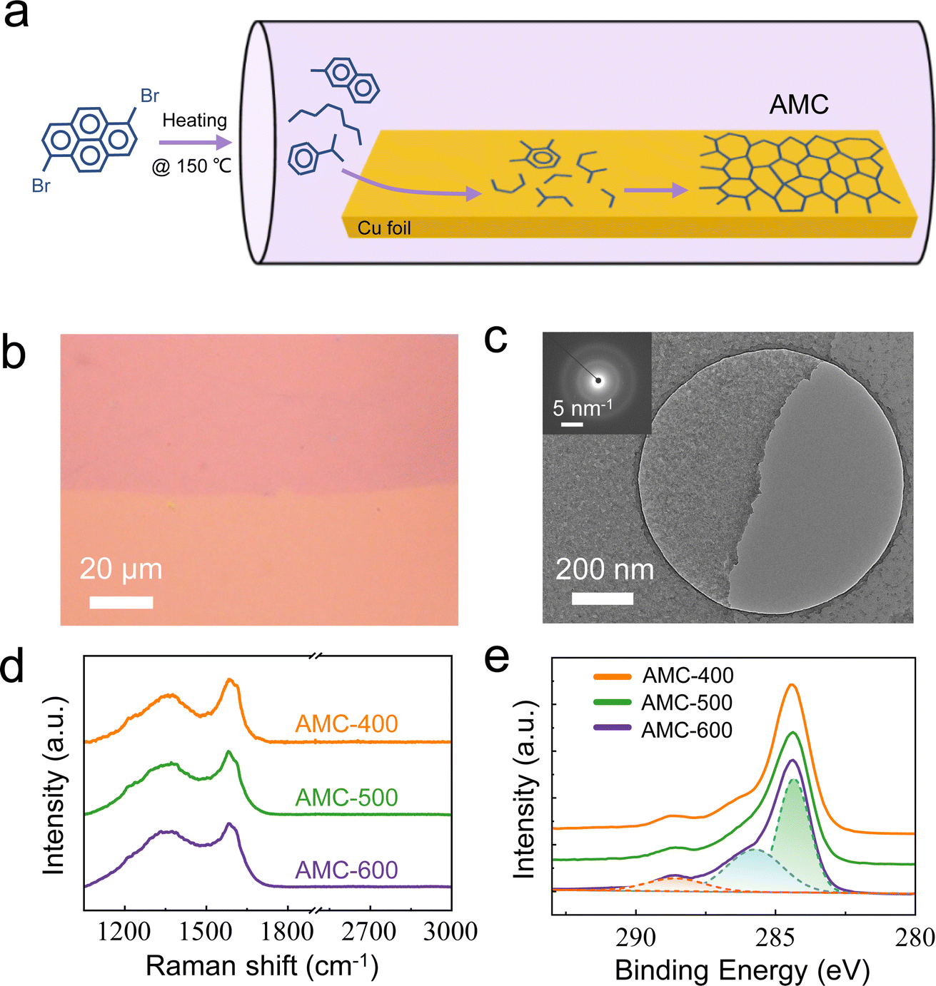 | ||
| Fig. 1 The synthesis and general characterizations of AMC. (a) Schematic of the AMC growth process, including the evaporation of 1,6-dibromopyrene, molecule cracking, species deposition, and aggregation to form a continuous film. (b) Optical microscopy image of one AMC-400 film after transferring onto a SiO2/Si substrate. (c) A low-magnification TEM image of AMC-600. (Inset) The diffraction pattern. (d) Raman spectra of AMC-400, AMC-500, and AMC-600. (e) XPS spectra of AMC-400, AMC-500 and AMC-600 with peak fittings. | ||
The polymer-assisted transfer process that has been well established for crystalline monolayers was carried out after the AMC growth. As displayed in Fig. 1b, after transferring it onto a SiO2/Si substrate, one can easily identify the AMC film as continuous with uniform optical contrast and full coverage. By the atomic force microscope (AFM) measurement, the apparent height of one as-transferred AMC film is ∼1 nm (Fig. S1†). No second islands/adlayers were found, suggesting a self-limited growth within 400–600 °C. A low-magnification transmission electron microscope (TEM) image is shown in Fig. 1c, indicating that the AMC-600 film has enough mechanical strength to be suspended on μm-sized holes of TEM grids. More importantly, the selected area electron diffraction (SAED) results are diffuse halos without any diffraction spots, further confirming its amorphous nature stemming from the low-temperature growth. Furthermore, by the Raman measurements, the vitreous characteristic of the AMC films is corroborated. As shown in Fig. 1d, all spectra from AMC-400, -500, and -600 samples are composed of broad D and G peaks located at ∼1350 cm−1 and 1590 cm−1, respectively, and more importantly, without any G′ signal around 2700 cm−1 (Fig. S2†). X-ray photoemission spectroscope (XPS) characterizations, as displayed in Fig. 1e, confirm the presence of dominant C–C (sp2-bonded, at ∼284.6 eV), C–O (at ∼286.1 eV), and C![[double bond, length as m-dash]](https://www.rsc.org/images/entities/char_e001.gif) O bonds (at ∼288.5 eV) in the AMC samples, with no significant differences ranging from AMC-400 to AMC-600 in terms of the peak positions and ratios.41 Moreover, the full scans of XPS measurements show no impurity of other elements in AMC samples (Fig. S3†). After more spectroscopic measurements, including the UV-Vis absorbance spectrum and photoluminescence spectrum,42 there is no apparent difference within the AMC samples (Fig. S4†).
O bonds (at ∼288.5 eV) in the AMC samples, with no significant differences ranging from AMC-400 to AMC-600 in terms of the peak positions and ratios.41 Moreover, the full scans of XPS measurements show no impurity of other elements in AMC samples (Fig. S3†). After more spectroscopic measurements, including the UV-Vis absorbance spectrum and photoluminescence spectrum,42 there is no apparent difference within the AMC samples (Fig. S4†).
While the above general materials characterizations confirmed the successful synthesis of AMC films with the commercial precursor, these tools acquiring the signals over the μm-large regions (or even larger) fall short in capturing the nm-scale features. We utilized scanning transmission electron microscopy (STEM) to directly visualize the atomic structures.43–45 As shown in Fig. 2a–c, one can feasibly observe the carbon atoms arranged by 5-, 6-, 7-, and 8-membered rings within a continuous monolayer with some contaminations inevitable from the transfer process and sample storage in air. These features agree well with those previously revealed in the AMC samples grown by the lab-synthesized, specific molecule.32 Moreover, we note that holes with diameters ranging from 0.2 to 1.5 nm can be found, and are insensitive to the selected regions. As displayed in Fig. 2a–c, AMC-400, AMC-450, and AMC-500 samples contain small nanopores (<1 nm) with an additional and the notable presence of large nanopores (>1 nm). We further analyzed a series of atomical images (a total of 1000 nm2), preliminarily revealing the distribution of nanopores with different-sized diameters across the temperature range that we selected. As summarized in Fig. 2d–f, AMC-400 shows nanopores up to ∼4 nm, while the maximum diameter shrinks to ∼2 nm in AMC-450 and falls below 1 nm for AMC-500 (Fig. S5†). Apparently, the fitting curve became narrower and shifted down to a small value when the growth temperature was increased. A quantitative evaluation of the pores' size and number is presented in Fig. 2g, highlighting the same temperature dependence. More specifically, compared to AMC-400, AMC-450 exhibits a rapid drop in the nanopore density and a modest decline in the mean pore diameter. AMC-500 continues this trend with a further decrease in both.
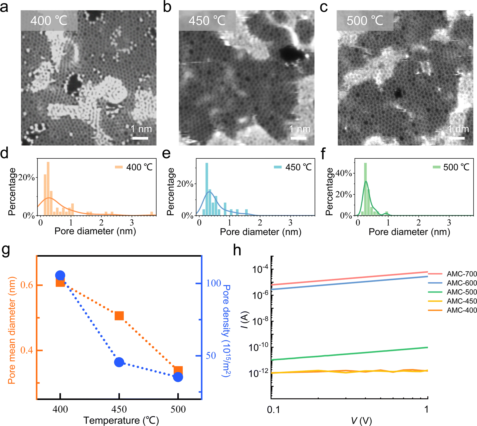 | ||
| Fig. 2 Atomic-scale STEM and electrical characterization of AMC obtained at different temperatures. (a–c) Representative STEM images of AMC-400 (a), AMC-450 (b) and AMC-500 (c). (d–f) Histogram of pore diameters in AMC-400 (d), AMC-450 (e) and AMC-500 (f) with fitted curves. (g) Statistics of pore mean diameters and pore densities of AMC. (h) Results from two-terminal electrical I–V measurements on AMC. | ||
Here, we note that while the STEM characterization provides the opportunity to understand the structural characteristics of AMC samples at the atomical level to ensure the atomic resolution, each atomic image is typically from a small region, for instance, ∼8.5 nm by 8.5 nm for Fig. 2a–c. Thus, the information from each atomic image has a “local” and random character. For a comprehensive comparison of the nanopore density and diameter, a large number of images is preferred, and more data sets can approach the real case well. However, it turns out to be a very laborious and challenging task to acquire atomic images by considering difficulties in preparing the clean, suspended TEM sample and maintaining its cleanliness during imaging.46 Although not from many data points, the results in Fig. 2d–g are the consequence of our greatest efforts. These results unambiguously confirm the growth-temperature-dependent nanopore in a qualitative (or even semiquantitative) way; thus, there are less and smaller nanopores at the higher growth temperature.
This conclusion naturally agrees with the common intuition. Back to the microscopic growth mechanism, for the growth of graphene on Cu, the temperature was typically at 1000 °C, much higher than that used here (400–600 °C), giving rise to abundant carbon species for the nucleation and growth, and sufficient mobility of these carbon fragments on Cu.36 However, as for the AMC synthesis, the temperature can be just a little bit higher than the cracking threshold of molecules (∼300 °C),32 leading to a finite carbon supply. Moreover, the carbon fragments experience a much lower mobility on Cu surfaces due to low temperatures. Both facts might lead to a situation that the diffusion-limit aggregation dominates, producing a porous configuration (Fig. S6†) rather than the seamless graphene film occurring at 1000 °C. From another point of view, one can treat the presence of nanopores in AMC as one type of disorder, and tuning the growth temperature can modulate DOD, including nanopores in terms of their density and size. As one evidence, the in-plane conductivity of two-terminal AMC devices is highly related to the growth temperature. As shown in Fig. 2h, increasing the growth temperature allows the device current to be tuned from 10−12 A to 10−4 A under the same device bias and dimension. This correspondence is believed to be bridged by DOD, mainly determined by the growth temperature.32
To unravel the underlying mechanisms behind the nanopore formation and its regulation in AMC, we developed a new kinetic Monte Carlo (KMC) simulation protocol based on a combined first-principles/force-field description (see details in the Method). The simulations are performed on the Cu(100) substrate (the same used in experiments), which consists of a supercell of 6 × 6 × 4 copper atoms. Ninety carbon atoms are randomly deposited on the substrate. These carbon atoms maintain a density equivalent to that of crystalline graphene. Starting from the initial arrangements, we employ KMC for annealing purposes. In this process, each particle is sequentially selected for movement in a single iteration. Every particle can move in one of four horizontal directions. The likelihood of moving in a particular direction is determined by the formula exp((Enow − Enext)/kBT), where Enow represents the energy of the current configuration, Enext denotes the energy of the configuration after the particle's movement, kB is the Boltzmann constant, and T is the temperature. We ensure the normalization of the probability distribution across all four directions. The simulation is conducted through over 6000 iterations, with the final analysis based on the average results obtained from iterations ranging between 5000th and 6000th. The carbon-surface interaction is fitted to the density functional theory calculation,47 while the carbon–carbon interaction is computed using the adaptive intermolecular reactive empirical bond-order (AIREBO) potential.48 To qualitatively capture the temperature dependence of nanopores, we set kBT values in KMC to 0.5 eV and 0.05 eV, corresponding to the higher and lower temperatures, respectively. We note that the significant temperature variance is unfortunately necessary due to the short time scales of atomistic simulations, and a similar high-temperature choice was suggested previously.33
Fig. 3a and b depict in the final iteration of the atomic configurations with highlighted carbon rings, including pentagons, hexagons, heptagons, and octagons/nonagons, by colors on a 6 × 6 copper surface at high and low kBT, respectively. Visibly, at high kBT, one can find more hexagons (labeled by pink) than that in the configuration obtained at low kBT. More importantly, no octagons/nonagons can be observed at high kBT, while these large-membered rings with the bigger hole size can be easily identified in AMC obtained at low kBT. All of these features indicate that at high kBT, the amorphous carbon tends to form a more compact structure with fewer large-sized defects, which agrees well with our experimental finding. Furthermore, we analyzed the distribution of ring types from the 5000th–6000th iteration. As shown in Fig. 3c, indeed at high kBT, the structure holds higher 6-membered rings and lower 8/9-membered ones when compared with that at low kBT.
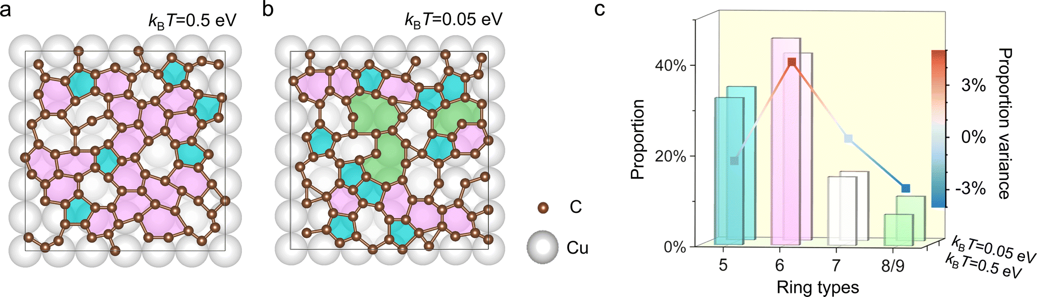 | ||
| Fig. 3 Monte Carlo simulation of AMC formation. (a and b) The atomic configurations of AMC on a 6 × 6 Cu (100) substrate at high kBT (0.5 eV, (a)) and low kBT (0.05 eV, (b)). Carbon pentagons (5-membered ring), hexagons (6-membered ring), heptagons (7-membered ring), and octagons/nonagons (8-/9-membered ring) are marked by cyan, pink, grey, and green, respectively. The carbon–carbon bonds are illustrated in gray, defined by a consistent cutoff distance of 1.89 Å. (c) Statistical diagram of proportions of each ring type for both high and low kBT situations. The color-coded legends represent the variance of proportions between two kBT conditions. | ||
Overall, the simulations reveal a high probability of carbon hexagons at the higher temperature, suggesting the formation of a more stable nucleus. Such a nucleus will likely result in more ordered AMC during the growth, consequently leading to smaller nanoporous regions. On the contrary, at the lower temperature, there is a noticeable increase in rings containing more than eight carbon atoms, which suggests a higher propensity for forming unoccupied crystalline sites and larger pores.
Distinguishing from the densely packed, defect-free structure in graphene, AMC with the presence of nanopores eliminates the need for additional pore creation for ionic transport functionality. As displayed in Fig. 4a, the AMC membrane is transferred onto a glass support with a 1 μm-diameter pore, completely covering the aperture. A 1 M KCl solution is added to both sides of the membrane, and electrodes are inserted to apply a potential, driving ions through the nanopores in AMC. The transmembrane current is then measured to calculate the conductance.18,23 As shown in Fig. 4b, the linear characteristics of the current-bias relationship are found for AMC-400, AMC-500, and AMC-600, revealing the ohmic behavior. However, the conductance, presented by the slopes, exhibits over one order of magnitude variation, that is, 23.7 nS for AMC-400, 0.8 nS for AMC-500, and 0.6 nS for AMC-600. Moreover, when using the same measurement procedures but with a smaller step size, the ionic transmembrane conductance behaviors of AMC-420, AMC-440, AMC-460, and AMC-480, have been investigated as well, showing a continuous and monotonic tuning (Fig. S7†). This conductance dependence in the growth temperature correlates very well with the temperature-tuned nanopores in AMC, which were corroborated above both experimentally and theoretically. The results from ionic transports confirmed the DOD-tuned functionality in AMC, introducing a new type of membrane material in which the nanopores intrinsically exist and are easily tuned by the growth temperature. Furthermore, benefiting from its monolayer nature, two AMC films can be stacked vertically as the membrane, which requires ions to traverse both layers. As displayed in Fig. 4c, small currents near the device limit are detected for bi-layer AMC membranes.
 | ||
| Fig. 4 Transmembrane ionic transport measurement of AMC. (a) Schematic illustration of the device setup. The AMC membrane covers a one-μm diameter glass hole with 1 M KCl on both sides of the membrane, with Ag/AgCl electrodes connected on either side to apply a bias voltage. (b) The transmembrane current versus bias curves of AMC-400, AMC-500 and AMC-600. (c) The transmembrane current versus bias curves of stacking samples. I–V curves for bi-AMC membranes composed of different layer combinations, where “+” denotes vertical stacking with the top layer listed first. (d) The transmembrane conductance of monolayer AMC and bi-layer AMCs, calculated I–V curves in (b) and (c), illustrating a wide range of tunability. | ||
For a comprehensive comparison, multiple devices (more than 25) have been tested, and the results are summarized in Fig. 4d. Pink and blue regions represent AMC and bi-layer AMC configurations, respectively. While AMC-400 holds the most significant conductance, increasing the synthesis temperature can effectively decrease the ions transport through AMC. Moreover, stacking two AMC layers introduces additional ion transport barriers, as the total ion conductance of stacked AMCs deviates from a simple series addition of individual conductance. For example, two AMC-400 layers (marked by 400 + 400) exhibit conductance as low as ∼0.4 nS, even lower than AMC-600. When coming to the microscopic mechanism, it is not surprising since nanopores in each layer are not necessarily aligned. Also, we note that the very high repeatability is suggested by a small error bar at each data point.
Unlike graphene or MoS2 membranes, which rely on external techniques like electron cyclotron resonance or electron irradiation for nanopore creation, AMC offers distinct advantages with its intrinsic nanopores (see the detailed comparison in Table S1†).18,21,25,49 Firstly, the inherent and tunable nature of AMC nanopores allows for dynamic conductance control over an extensive range, which is two (eight) times larger than that of MoS2 (graphene) within the 400–600 °C temperature window.25,49 Secondly, direct stacking of the AMC layers enables further tailoring of conductance, leading to an even broader tunability (totally over two orders of magnitude). This versatility of AMC membranes, coupled with their inherent ion transport capabilities, makes them very promising for various nanofluidic applications. Additionally, we notice that monolayer amorphous carbon could be prepared by plasma- and laser-assisted CVD contains defects like eight-atom rings but without nanopores, thus offering a very different material when compared with AMC here.33 The underlying origin could be the harsh growth conditions, for example, plasma and laser, that facilitate the healing of nanopores, if having any, by the effective etching and re-growth process.50
Due to its vitreous and monolayer nature, one don't expect AMC as stable as graphene. In our experiments, the AMC films survived after the whole process, sequentially including the underlying Cu etching, PMMA-assisted transfer and the removal of PMMA, and the ionic conductance measurements. We have to note that, since it is one of the carbon nanomaterials (new type, when compared with well-known others, such as graphene, carbon nanotube, and fullerene, Fig. S8†) and full of defects, its tolerance to oxygen gas at high temperatures (e.g., >200 °C) would be inferior, which has been experimentally confirmed in the previous study,32 and this instability isn't taken into account seriously when talking about its application in the transmembrane. Moreover, it could be an interesting topic when compared AMC with other amorphous carbon nanomaterials, such as amorphous carbon quantum dots (CQDs).51 CQDs with typical sizes of 1–10 nm is a zero-dimension material and possesses size-dependent absorption and emission,52 while AMC is a 2D material without significant optical response as shown in Fig. S4.† As for the fabrications, there are several successful ways to prepare CQDs,53 and the CVD method has proven effective to synthesize AMC. Moreover, CQDs have been demonstrated in the applications of bioimaging, sensing, drug delivery, and catalysis,54–57 while the applications of AMC have been largely unexplored.
3. Conclusion
In summary, we demonstrated the growth temperature-tuned DOD in nanopore and ionic transport. With the commercially available precursors, AMC films with different DODs can be straightforwardly obtained by thermal CVD. Atomic structural characterizations reveal that AMC films grown at various temperatures exhibit varying nanopore sizes and densities, revealing the tunable DOD. The kinetic Monte Carlo simulations corroborate the existence of nanopores in AMC and its temperature dependence. The ionic transport measurements further confirm its tunability in nanopores by a wide range of transmembrane ion conductance. Moreover, the transfer-stacking technique commonly unitized in 2D materials allows the bilayer AMC to regulate the ionic transport further. Our results introduce a DOD-tuned membrane material, holding immense potential for novel nanodevices and filtration technologies through strategic nanopore manipulations, unlocking 2D amorphous materials' applications in mass separation, energy storage, and sensing.304. Methods
4.1 Sample synthesis and transfer
To prepare AMC samples, copper foils (Alfa Aesar, 25 μm thick) were pre-the starting material was treated in dilute HNO3 for 5 s and deionized (DI) water for 10 s. They were then annealed at 1000 °C under Ar/H2 flow (20 vol% H2) for 30 min. After cooling, the commercial precursor, 1,6-dibromopyrene, was introduced to an upstream heating zone powered by a heating tape. In the growth zone, copper foils were heated to 400–700 °C under H2 flow, while the precursor, evaporated at 150 °C, was carried to the zone. After an 8 minute growth, heating was stopped, and the samples were rapidly cooled. Prior to transfer, SiO2/Si substrates (crystal applied) were cleaned with acetone and isopropanol (IPA), followed by oxygen plasma treatment. Glass chips (1 μm pore diameter, nano-patch-clamp chips, Nanion) were rinsed in DI water and ethanol, then treated with oxygen plasma. For the PMMA-assisted transfer process, AMC on copper foil was first spin-coated with polymethyl methacrylate (PMMA) and heated at 160 °C for 2 min. FeCl3 solution (1 M, Transene) was used to etch away the copper foil, and the “PMMA layer + AMC layer” was washed repeatedly with HCl solution (36%) and DI water, followed by the transfer onto SiO2/Si substrates or glass chips. Finally, PMMA was removed with acetone. The direct transfer process of AMC samples is as follows. AMC on copper foil was placed face-to-face with an Au grid (quatrefoil, EM Resolutions). IPA was dropped on the sample and evaporated, facilitating direct contact between AMC and the grid. Na2S2O8 solution (1 M) was used to etch away the copper foil, leaving AMC on the grid. Finally, DI water was employed to wash the sample several times. For the bilayer AMC, a floating AMC (top layer) was prepared with PMMA spin-coating, FeCl3 etching, and HCl/DI water washing. Then, the “PMMA layer + top-AMC layer” was placed on a bottom AMC and heated for close contact. The FeCl3/HCl/DI water treatment yielded “PMMA layer + AMC double layers”. Finally, the samples were scooped out with glass chips, and PMMA was removed by the acetone bath.4.2 Characterizations
Raman spectra (532 nm) were obtained using a Horiba iHR320 spectrometer with a SmartRaman module. X-ray photoelectron spectroscopy (XPS) measurements were performed using an AXIS Ultra DLD system and analyzed with XPSPEAK software. AFM (Scansyst mode, Bruker Dimension ICON) was employed to measure AMC height on SiO2/Si substrates. TEM and SAED characterizations were performed in JEOL JEM-ARM300F under 80 kV. STEM characterizations were performed by Nion U-HERMES100 under 60 kV.4.3 Device fabrication and electrical measurements
To create AMC devices on SiO2/Si substrates, an electron-beam lithography (Tescan) microfabrication process was employed. Reactive ion etching (ME-3A) was conducted to make patterns, followed by thermal evaporation (ZHD400) to deposit metal electrodes of In (10 nm)/Au (40 nm). After the lift-off procedure, in-plane I–V measurements were performed using a vacuum probe station with Keithley 2614B SourceMeters. For ionic transmembrane transport measurements, AMC membranes on glass chips were glued (Flexbar Reprorubber) to pools on both sides. After filling the pools with 1 M KCl solution, two Ag/AgCl electrodes were inserted in the top and bottom pools. Electrodes were connected to an ultralow-noise patch clamp amplifier (Axopatch 200B, Axon) and analog-to-digital converter (Digidata 1550B, Axon) for the bias introduction and transmembrane current detection.4.4 Theoretical calculations
In our kinetic Monte Carlo simulation, we approximate the system's energy by dividing it into two primary components: the interaction energy between the substrate and carbon atoms and the carbon–carbon interaction energy. For the interaction between the substrate and carbon atoms, we discretize the substrate surface into a 60 × 60 grid. Using the Vienna ab initio Simulation Package (VASP)58 and employing density functional theory, we calculate the energies at selected sites involving the substrate and individual carbon atoms. The Perdew–Burke–Ernzerhof (PBE) exchange correlation functional is chosen to describe the electron interaction.47 The projector augmented wave method is used with an energy cutoff of 400 eV.59 A k-point mesh of 2 × 2 × 1 is used for the reciprocal space sampling. The interpolation method is employed, taking the lattice periodicity of copper into account, to estimate the potential energy for a single carbon atom at all grid sites. Regarding the carbon–carbon interaction, we describe it using the adaptive intermolecular reactive empirical bond-order potential (AIREBO),48 as implemented in the Large-scale Atomic/Molecular Massively Parallel Simulator (LAMMPS) molecular dynamics program.60Author contributions
L. L. and W. F. conceived and supervised the project. S. L., H. T., and Z. L. synthesized the samples. S. L., Z. Y., R. L., P. L., Y. W., L. Y. Z., G. Y., and U. S. performed the general characterizations and sample transfer. S. L. and Z. L. performed the electrical measurements. H. T., J. G., and L. W. performed the TEM and SAED measurements. Y. M. and W. Z. performed the STEM measurements. S. L., R. C., H. X., and X. Z. performed the ionic transport measurements. J. H. and J. C. performed the theoretical calculations. S. L., J. H., J. C., and L. L. wrote the manuscript, and all authors discussed and commented on it.Conflicts of interest
There are no conflicts to declare.Acknowledgements
This work was supported by the National Key R&D Program of China (2018YFA0305800, 2021YFA1400500) and the Beijing Natural Science Foundation (JQ23004). L. W. is grateful for the support from the Youth Innovation Promotion Association of CAS (2020009). Computational resources were offered by the Peking University supercomputing platform. L. L. acknowledges the support of facilities from Peking Nanofab.References
- I. E. Roslon, R. J. Dolleman, H. Licona, M. Lee, M. Siskins, H. Lebius, L. Madauss, M. Schleberger, F. Alijani, H. S. J. van der Zant and P. G. Steeneken, Nat. Commun., 2020, 11, 6025 CrossRef CAS PubMed.
- J. Wang, C. Cheng, X. Zheng, J. C. Idrobo, A. Y. Lu, J. H. Park, B. G. Shin, S. J. Jung, T. Zhang, H. Wang, G. Gao, B. Shin, X. Jin, L. Ju, Y. Han, L. J. Li, R. Karnik and J. Kong, Nature, 2023, 623, 956–963 CrossRef CAS PubMed.
- R. H. Tunuguntla, R. Y. Henley, Y. C. Yao, P. Tuan Anh, M. Wanunu and A. Noy, Science, 2017, 357, 792–796 CrossRef CAS PubMed.
- M. Macha, S. Marion, V. V. R. Nandigana and A. Radenovic, Nat. Rev. Mater., 2019, 4, 588–605 CrossRef CAS.
- H. Wang, L. M. Su, M. Yagmurcukardes, J. W. Chen, Y. Jiang, Z. Li, A. C. Quan, F. M. Peeters, C. Wang, A. K. Geim and S. Hu, Nano Lett., 2020, 20, 8634–8639 CrossRef CAS PubMed.
- A. Siria, P. Poncharal, A. L. Biance, R. Fulcrand, X. Blase, S. T. Purcell and L. Bocquet, Nature, 2013, 494, 455–458 CrossRef CAS PubMed.
- Y. C. Liu, L. H. Yeh, M. J. Zheng and K. C. W. Wu, Sci. Adv., 2021, 7, eabe9924 CrossRef CAS PubMed.
- J. Clarke, H. C. Wu, L. Jayasinghe, A. Patel, S. Reid and H. Bayley, Nat. Nanotechnol., 2009, 4, 265–270 CrossRef CAS PubMed.
- P. Xie, Q. H. Xiong, Y. Fang, Q. Qing and C. M. Lieber, Nat. Nanotechnol., 2012, 7, 119–125 CrossRef CAS PubMed.
- J. D. Feng, K. Liu, R. D. Bulushev, S. Khlybov, D. Dumcenco, A. Kis and A. Radenovic, Nat. Nanotechnol., 2015, 10, 1070–1076 CrossRef CAS PubMed.
- S. J. Heerema and C. Dekker, Nat. Nanotechnol., 2016, 11, 127–136 CrossRef CAS PubMed.
- L. Wang, M. S. H. Boutilier, P. R. Kidambi, D. Jang, N. G. Hadjiconstantinou and R. Karnik, Nat. Nanotechnol., 2017, 12, 509–522 CrossRef CAS PubMed.
- M. Graf, M. Lihter, M. Thakur, S. Georgiou, J. Topolancik, B. R. Ilic, K. Liu, J. D. Feng, Y. Astier and A. Radenovic, Nat. Protoc., 2019, 14, 1130–1168 CrossRef CAS PubMed.
- S. Hu, M. Lozada-Hidalgo, F. C. Wang, A. Mishchenko, F. Schedin, R. R. Nair, E. W. Hill, D. W. Boukhvalov, M. I. Katsnelson, R. A. W. Dryfe, I. V. Grigorieva, H. A. Wu and A. K. Geim, Nature, 2014, 516, 227–230 CrossRef CAS PubMed.
- P. Z. Sun, Q. Yang, W. J. Kuang, Y. V. Stebunov, W. Q. Xiong, J. Yu, R. R. Nair, M. I. Katsnelson, S. J. Yuan, I. V. Grigorieva, M. Lozada-Hidalgo, F. C. Wang and A. K. Geim, Nature, 2020, 579, 229–232 CrossRef CAS PubMed.
- L. F. Wang, J. Chen, S. J. Cox, L. Liu, G. C. Sosso, N. Li, P. Gao, A. Michaelides, E. G. Wang and X. D. Bai, Phys. Rev. Lett., 2021, 126, 136001 CrossRef CAS PubMed.
- L. F. Wang, L. Liu, J. Chen, A. Mohsin, J. H. Yum, T. W. Hudnall, C. W. Bielawski, T. Rajh, X. D. Bai, S. P. Gao and G. Gu, Angew. Chem., Int. Ed., 2020, 59, 15734–15740 CrossRef CAS PubMed.
- S. Garaj, W. Hubbard, A. Reina, J. Kong, D. Branton and J. A. Golovchenko, Nature, 2010, 467, 190–193 CrossRef CAS.
- S. P. Surwade, S. N. Smirnov, I. V. Vlassiouk, R. R. Unocic, G. M. Veith, S. Dai and S. M. Mahurin, Nat. Nanotechnol., 2016, 11, 995 CrossRef CAS PubMed.
- G. F. Schneider, S. W. Kowalczyk, V. E. Calado, G. Pandraud, H. W. Zandbergen, L. M. K. Vandersypen and C. Dekker, Nano Lett., 2010, 10, 3163–3167 CrossRef CAS PubMed.
- S. K. Min, W. Y. Kim, Y. Cho and K. S. Kim, Nat. Nanotechnol., 2011, 6, 162–165 CrossRef CAS PubMed.
- F. Traversi, C. Raillon, S. M. Benameur, K. Liu, S. Khlybov, M. Tosun, D. Krasnozhon, A. Kis and A. Radenovic, Nat. Nanotechnol., 2013, 8, 939–945 CrossRef CAS PubMed.
- X. Zhang, P. M. G. van Deursen, W. Fu and G. F. Schneider, ACS Sens., 2020, 5, 2317–2325 CrossRef CAS PubMed.
- J. Feng, K. Liu, M. Graf, M. Lihter, R. D. Bulushev, D. Dumcenco, D. T. L. Alexander, D. Krasnozhon, T. Vuletic, A. Kis and A. Radenovic, Nano Lett., 2015, 15, 3431–3438 CrossRef CAS PubMed.
- J. Feng, M. Graf, K. Liu, D. Ovchinnikov, D. Dumcenco, M. Heiranian, V. Nandigana, N. R. Aluru, A. Kis and A. Radenovic, Nature, 2016, 536, 197–200 CrossRef CAS PubMed.
- H. Qi, Z. Li, Y. Tao, W. Zhao, K. Lin, Z. Ni, C. Jin, Y. Zhang, K. Bi and Y. Chen, Nanoscale, 2018, 10, 5350–5357 RSC.
- C. J. Russo and J. A. Golovchenko, Proc. Natl. Acad. Sci. U. S. A., 2012, 109, 5953–5957 CrossRef CAS PubMed.
- J. P. Fried, J. L. Swett, B. P. Nadappuram, J. A. Mol, J. B. Edel, A. P. Ivanov and J. R. Yates, Chem. Soc. Rev., 2021, 50, 4974–4992 RSC.
- R. Zallen, The Physics of Amorphous Solids, 2008 Search PubMed.
- H. Tian, Z. Yao, Z. Li, J. Guo and L. Liu, ACS Nano, 2023, 17, 24468–24478 CrossRef CAS PubMed.
- L. Liu, Chin. Phys. Lett., 2023, 40, 56101 CrossRef.
- H. Tian, Y. Ma, Z. Li, M. Cheng, S. Ning, E. Han, M. Xu, P. F. Zhang, K. Zhao, R. Li, Y. Zou, P. Liao, S. Yu, X. Li, J. Wang, S. Liu, Y. Li, X. Huang, Z. Yao, D. Ding, J. Guo, Y. Huang, J. Lu, Y. Han, Z. Wang, Z. G. Cheng, J. Liu, Z. Xu, K. Liu, P. Gao, Y. Jiang, L. Lin, X. Zhao, L. Wang, X. Bai, W. Fu, J. Y. Wang, M. Li, T. Lei, Y. Zhang, Y. Hou, J. Pei, S. J. Pennycook, E. Wang, J. Chen, W. Zhou and L. Liu, Nature, 2023, 615, 56–61 CrossRef CAS PubMed.
- C. T. Toh, H. Zhang, J. Lin, A. S. Mayorov, Y. P. Wang, C. M. Orofeo, D. B. Ferry, H. Andersen, N. Kakenov, Z. Guo, I. H. Abidi, H. Sims, K. Suenaga, S. T. Pantelides and B. Ozyilmaz, Nature, 2020, 577, 199–203 CrossRef CAS PubMed.
- S. Hong, C. S. Lee, M. H. Lee, Y. Lee, K. Y. Ma, G. Kim, S. I. Yoon, K. Ihm, K. J. Kim, T. J. Shin, S. W. Kim, E. C. Jeon, H. Jeon, J. Y. Kim, H. I. Lee, Z. Lee, A. Antidormi, S. Roche, M. Chhowalla, H. J. Shin and H. S. Shin, Nature, 2020, 582, 511–514 CrossRef CAS PubMed.
- Y. M. He, L. R. Liu, C. Zhu, S. S. Guo, P. Golani, B. Koo, P. Y. Tang, Z. Q. Zhao, M. Z. Xu, P. Yu, X. Zhou, C. T. Gao, X. W. Wang, Z. D. Shi, L. Zheng, J. F. Yang, B. Shin, J. Arbiol, H. G. Duan, Y. H. Du, M. Heggen, R. E. Dunin-Borkowski, W. L. Guo, Q. J. Wang, Z. H. Zhang and Z. Liu, Nat. Catal., 2022, 5, 212–221 CrossRef CAS.
- L. Liu, J. Park, D. A. Siegel, K. F. McCarty, K. W. Clark, W. Deng, L. Basile, J. C. Idrobo, A. P. Li and G. Gu, Science, 2014, 343, 163–167 CrossRef CAS.
- L. Liu, D. A. Siegel, W. Chen, P. Z. Liu, J. J. Guo, G. Duscher, C. Zhaog, H. Wang, W. L. Wang, X. D. Bai, K. F. McCarty, Z. Y. Zhang and G. Gu, Proc. Natl. Acad. Sci. U. S. A., 2014, 111, 16670–16675 CrossRef CAS PubMed.
- A. Mohsin, L. Liu, P. Z. Liu, W. Deng, I. N. Ivanov, G. L. Li, O. E. Dyck, G. Duscher, J. R. Dunlap, K. Xiao and G. Gu, ACS Nano, 2013, 7, 8924–8931 CrossRef CAS PubMed.
- J. J. Liu, R. J. Li, H. Li, Y. F. Li, J. H. Yi, H. C. Wang, X. C. Zhao, P. Z. Liu, J. J. Guo and L. Liu, New Carbon Mater., 2018, 33, 481–492 CrossRef CAS.
- H. Wang, C. Zhao, L. Liu, Z. Xu, J. K. Wei, W. L. Wang, X. D. Bai and E. G. Wang, Nano Res., 2016, 9, 1221–1235 CrossRef CAS.
- L. Liu, D. Xie, M. Wu, X. Yang, Z. Xu, W. Wang, X. Bai and E. Wang, Carbon, 2012, 50, 3039–3044 CrossRef CAS.
- R. Li, Y. Li, Y. Yang, X. Huang, S. Zhang, H. Tian, X. Huang, Z. Yao, P. Liao, S. Yu, S. Liu, Z. Li, Y. Huang, J. Guo, F. Mei, L. Wang, X. Li and L. Liu, ACS Appl. Nano Mater., 2021, 4, 13708–13715 CrossRef CAS.
- P. Z. Liu, H. F. Tian, W. Windl, G. Gu, G. Duscher, Y. C. Wu, M. Zhao, J. J. Guo, B. S. Xu and L. Liu, Nanoscale, 2019, 11, 20676–20684 RSC.
- A. Mohsin, N. G. Cross, L. Liu, K. Watanabe, T. Taniguchi, G. Duscher and G. Gu, 2D Mater., 2018, 5, 015007 CrossRef.
- A. Mohsin, N. G. Cross, L. Liu, P. Z. Liu, G. Duscher and G. Gu, Phys. Status Solidi B, 2017, 254, 1700069 CrossRef.
- N. Li, X. D. Guo, X. X. Yang, R. S. Qi, T. Y. Qiao, Y. F. Li, R. C. Shi, Y. H. Li, K. H. Liu, Z. Xu, L. Liu, F. J. G. de Abajo, Q. Dai, E. G. Wang and P. Gao, Nat. Mater., 2021, 20, 43–48 CrossRef CAS PubMed.
- J. P. Perdew, K. Burke and M. Ernzerhof, Phys. Rev. Lett., 1996, 77, 3865–3868 CrossRef CAS PubMed.
- S. J. Stuart, A. B. Tutein and J. A. Harrison, J. Chem. Phys., 2000, 112, 6472–6486 CrossRef CAS.
- T. Jain, B. C. Rasera, R. J. S. Guerrero, M. S. H. Boutilier, S. C. O'Hern, J.-C. Idrobo and R. Karnik, Nat. Nanotechnol., 2015, 10, 1053–1057 CrossRef CAS PubMed.
- E. Griffin, L. Mogg, G. P. Hao, G. Kalon, C. Bacaksiz, G. Lopez-Polin, T. Y. Zhou, V. Guarochico, J. H. Cai, C. Neumann, A. Winter, M. Mohn, J. H. Lee, J. H. Lin, U. Kaiser, I. V. Grigorieva, K. Suenaga, B. Ozyilmaz, H. M. Cheng, W. C. Ren, A. Turchanin, F. M. Peeters, A. K. Geim and M. Lozada-Hidalgo, ACS Nano, 2020, 14, 7280–7286 CrossRef CAS PubMed.
- S. Y. Lim, W. Shen and Z. Gao, Chem. Soc. Rev., 2015, 44, 362–381 RSC.
- N. Fuyuno, D. Kozawa, Y. Miyauchi, S. Mouri, R. Kitaura, H. Shinohara, T. Yasuda, N. Komatsu and K. Matsuda, Adv. Opt. Mater., 2014, 2, 983–989 CrossRef CAS.
- X. Y. Xu, R. Ray, Y. L. Gu, H. J. Ploehn, L. Gearheart, K. Raker and W. A. Scrivens, J. Am. Chem. Soc., 2004, 126, 12736–12737 CrossRef CAS PubMed.
- L. Cao, X. Wang, M. J. Meziani, F. S. Lu, H. F. Wang, P. J. G. Luo, Y. Lin, B. A. Harruff, L. M. Veca, D. Murray, S. Y. Xie and Y. P. Sun, J. Am. Chem. Soc., 2007, 129, 11318–11319 CrossRef CAS PubMed.
- W. Shi, X. Li and H. Ma, Angew. Chem., Int. Ed., 2012, 51, 6432–6435 CrossRef CAS PubMed.
- M. Zheng, S. Liu, J. Li, D. Qu, H. F. Zhao, X. G. Guan, X. L. Hu, Z. G. Xie, X. B. Jing and Z. C. Sun, Adv. Mater., 2014, 26, 3554–3560 CrossRef CAS PubMed.
- H. T. Li, X. D. He, Z. H. Kang, H. Huang, Y. Liu, J. L. Liu, S. Y. Lian, C. H. A. Tsang, X. B. Yang and S. T. Lee, Angew. Chem., Int. Ed., 2010, 49, 4430–4434 CrossRef CAS PubMed.
- G. Kresse and J. Furthmuller, Phys. Rev. B: Condens. Matter Mater. Phys., 1996, 54, 11169–11186 CrossRef CAS PubMed.
- P. E. Blöchl, Phys. Rev. B: Condens. Matter Mater. Phys., 1994, 50, 17953 CrossRef PubMed.
- S. Plimpton, J. Comput. Phys., 1995, 117, 1–19 CrossRef CAS.
Footnotes |
| † Electronic supplementary information (ESI) available. See DOI: https://doi.org/10.1039/d4ra01523a |
| ‡ These authors contributed equally to this work. |
| This journal is © The Royal Society of Chemistry 2024 |