
Enhanced transparent conducting performance of c-axis oriented Ca3Co4O9 thin films†
Guangsheng Fuab,
Guoying Yanab,
Liqing Sunb,
Hongrui Zhangbc,
Haizhong Guoc,
Jianglong Wangb and
Shufang Wang*b
aSchool of Information Engineering, Hebei University of Technology, Tianjin 300401, China
bHebei Key Lab of Optic-electronic Information and Materials, The College of Physics Science and Technology, Hebei University, Baoding 071002, China. E-mail: swang2008@hotmail.com; sfwang_researcher@aliyun.com; Fax: +86-312-5077370; Tel: +86-312-5077370
cBeijing National Laboratory for Condensed Matter & Institute of Physics, Chinese Academy of Sciences, Beijing 100190, China
First published on 5th March 2015
Abstract
p-type transparent conductive Ca3Co4O9 thin films were grown on LaAlO3 substrates using a pulsed laser deposition technique. The films showed perfect c-axis orientation with a resistivity of about 7.3 mΩ cm at room temperature and optical transmittance of about 50% in the visible range. A high figure of merit of about 988 MΩ−1 was achieved in these c-axis oriented Ca3Co4O9 films, which is comparable to those reported for the state-of-the-art p-type transparent conducting oxides. This work demonstrated the potential applications of c-axis oriented Ca3Co4O9 films in optoelectronic devices as a new class of transparent conducting oxide coatings.
Introduction
Transparent conducting oxides (TCOs) are electrical conductive materials with a high transparency to visible light. They are widely used as the electrodes or coatings of many optoelectronic devices such as solar cells, light emitting diodes and flat panel displays. The most commonly used TCOs, for example, tin oxide (SnO2), indium oxide (In2O3), indium tin oxide (ITO), and zinc oxide (ZnO), are primarily n-type semiconductors.1–3 Compared to conventional n-type TCOs, p-type TCOs are generally less conductive and less transparent, and therefore have not been largely commercialized yet. In order to fully explore the novel applications of TCOs in optoelectronic devices, the development of p-type TCOs is critical as well.4 In the past decade, delafossite compound CuMO2 (M = Cr, Al, Ga, Fe, Sc, Y), NiO, Cr2O3, MoO3 and etc. have been extensively studied as promising candidates of p-type TCOs.5–11R. D. Robinson et al. recently demonstrated that the misfit layered cobalt oxide Ca3Co4O9, a class of newly discovered p-type oxide thermoelectric material, exhibited very good transparent conducting performance.12 Their solution-processed randomly oriented polycrystalline Ca3Co4O9 thin films showed the best figure of merit FOM of about 151 MΩ−1, which was higher than the values reported in literatures for most other p-type TCO thin films. Here, the figure of merit FOM is usually used to evaluate the performance of TCOs and it is defined as −1/(Rsh × ln![[thin space (1/6-em)]](https://www.rsc.org/images/entities/char_2009.gif) T), where Rsh is the sheet resistance and T is the average optical transmittance, respectively.10 It is known that the crystal structure of Ca3Co4O9 consists of the conducting CoO2 layer and the insulating Ca2CoO3 layer, which are alternately stacked along the c-axis. This layered structure results in a large anisotropy of the electrical transport properties with the ab-plane electrical conductivity being much larger than that along the c-axis.13 Moreover, randomly oriented polycrystalline thin films always contain many defects such as grain boundaries and dislocations, which will lead to a small charge carrier mobility and thus a low electrical conductivity.6 Very recently, Xuebin Zhu et al. reported that the solution-processed c-axis oriented Bi2Sr2Co2Oy thin films, another type of misfit layered cobalt oxide with the crystal structure being similar to that of the Ca3Co4O9, showed an enhanced FOM in comparison with that of the polycrystalline Ca3Co4O9 thin films.14 This experimental result provided valuable insights on the improvement in the performance of this new class of p-type TCO coatings.
T), where Rsh is the sheet resistance and T is the average optical transmittance, respectively.10 It is known that the crystal structure of Ca3Co4O9 consists of the conducting CoO2 layer and the insulating Ca2CoO3 layer, which are alternately stacked along the c-axis. This layered structure results in a large anisotropy of the electrical transport properties with the ab-plane electrical conductivity being much larger than that along the c-axis.13 Moreover, randomly oriented polycrystalline thin films always contain many defects such as grain boundaries and dislocations, which will lead to a small charge carrier mobility and thus a low electrical conductivity.6 Very recently, Xuebin Zhu et al. reported that the solution-processed c-axis oriented Bi2Sr2Co2Oy thin films, another type of misfit layered cobalt oxide with the crystal structure being similar to that of the Ca3Co4O9, showed an enhanced FOM in comparison with that of the polycrystalline Ca3Co4O9 thin films.14 This experimental result provided valuable insights on the improvement in the performance of this new class of p-type TCO coatings.
Inspired by the above studies, we report here the significant enhancement in the transport conducting performance of Ca3Co4O9 thin films by improving its c-axis texture degree. High quality Ca3Co4O9 thin films with perfect c-axis orientation were successfully grown on LaAlO3 single crystal substrate by pulsed laser deposition technique. The obtaining films showed a low resistivity of about 7.3 mΩ cm at room temperature and a reasonable optical transmittance of about 50% in the visible range, resulting in a very high figure of merit of 998 MΩ−1. This FOM value is almost 6–7 times higher than that of the solution-processed polycrystalline thin film samples and is also comparable to the best values of other p-type TCOs so far reported in literatures.5–11
Experiments
c-axis oriented Ca3Co4O9 thin films were grown on single crystal LaAlO3 (001) substrates by pulsed laser ablation of a Ca3Co4O9 ceramic target at the substrate temperature of 680 °C under the oxygen pressure about 40 mtorr. The Ca3Co4O9 target used in this work was synthesized in air using the conventional solid-state reaction method. The commercial CaCO3 (99.5%, Alfa Aesar) and Co3O4 powders (99.7%, Alfa Aesar) were used as the starting materials. After fully grinding, the mixed powders were calcined at 600 °C for 5 h in air and then pressed into a round pellet (ϕ = 30 mm) under 10 MPa. The pellet was first sintered at 890 °C for 10 h in air with a furnace, and then it was reground, pelletized, and sintered for another 10 h at 890 °C in air. An excimer laser with 308 nm radiation was used for the film deposition with a laser energy density of 1.5 J cm−2 and a repetition rate of 3 Hz. The distance between the target and the substrate was about 50 mm. After deposition, the films were post-annealed at 820 °C for 60 min under the flowing of high-purity oxygen. The crystal structure of the films was measured using a Bruker AXS D8 advance X-ray diffractometer with Cu Kα radiation. The surface morphology of the films was analyzed by scanning electron microscopy (SEM). The microstructure and the elemental compositions of the films were analyzed with a field-emission transmission electron microscopy (TEM, Tecnai G2 F20) equipped with an energy-dispersive X-ray spectroscopy (EDS) detector. Resistivity measurements were performed by using a physical properties measurement system (PPMS, Quantum Design Inc.). The standard four point probe method was used to measure ab-plane resistivity of the Ca3Co4O9 film. To make the ohmic contact, four platinum electrodes (0.5 mm diameter) were deposited onto the films via thermal evaporation. The optical transmission was measured by using a Hitachi UH4150 UV-Visible-NIR spectrophotometer.Results and discussion
The X-ray diffraction (XRD) θ–2θ scan curve of a 50 nm-thick Ca3Co4O9 films on LaAlO3 substrates is shown in Fig. 1a. Besides the peaks from LaAlO3 substrate, only peaks from diffractions of (00l) Ca3Co4O9 planes are observed, and no diffraction peaks from secondary phases or randomly oriented grains are observed, indicating that the thin films are nearly perfect c-axis orientation with pure phase. The ω scan of the Ca3Co4O9 (004) peak, shown in inset of Fig. 1a, shows a full width at half maximum (FWHM) of 0.21, further confirming the excellent c-axis orientation of the film. Fig. 1b is the surface SEM image of the c-axis oriented Ca3Co4O9 film. The present film looks much smoother and denser than the corresponding polycrystalline films fabricated by solution method, where micro-scale cracks and nano-scale voids were clearly observed which deteriorated the electrical conductivity as well as the optical transmission of the films.12 | ||
| Fig. 1 (a) XRD θ–2θ scan of a 50 nm thick Ca3Co4O9 thin film on LaAlO3 substrate; (b) SEM surface image of Ca3Co4O9 thin film. | ||
The good crystalline quality and c-axis oriented growth of the Ca3Co4O9 thin films were further investigated by TEM. A bright field cross sectional TEM image displayed in Fig. 2a shows that the film is about 50 nm. The selected area electron diffraction (SAED) pattern taken from the film part is shown in the inset of Fig. 2a. The sharp electron diffraction spots with no satellites suggest that the film has good single crystallinity. Fig. 2b shows the high-resolution TEM image of the Ca3Co4O9 film near the interface. Well-ordered layer structures of Ca3Co4O9 stacked along the c axis can be clearly observed near the interface and everywhere inside the Ca3Co4O9 films. The c-axis lattice constant is about 1.08 nm, which is similar to previous results reported by other research groups. In addition, the interface appears very flat, and there is no obvious evidence of secondary phases or any chemical reaction in the interface region over large distances.
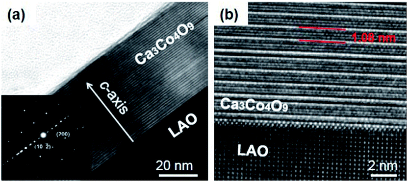 | ||
| Fig. 2 (a) TEM and (b) high resolution TEM of Ca3Co4O9/LaAlO3 (LAO) interface. The inset of (a) is the SAED pattern taken from the film part. The location of the CoO2 layers is indicated by red lines in (b), while the Ca2CoO3 layer locates between the two adjacent CoO2 layers. | ||
Elemental analysis and chemical characterization of the film sample were studied using TEM-EDS. The presence of Ca3Co4O9 with homogeneous distribution of Ca, Co, and O ions has been verified by EDS element mapping, as shown in Fig. 3. No other impurities were detected within the films. The EDS analysis of the inner regions of film reveals that the cation ion ratio of Ca:Co is about 3.00:4.18, which is very close to that of the nominal composition of this material. Moreover, the EDS element mapping also demonstrates that the interface is flat and no obvious interdiffusion occurs between the film and substrate. We also performed the EDS measurement on a large scale of SEM surface image of the present film. It showed the Ca:Co on the film surface was about 3.00:3.90. The Ca:Co ratio on the film surface is slightly larger than that in the inner regions of the film, indicating Ca migration to the film surface.
 | ||
| Fig. 3 TEM-EDS map of Ca3Co4O9 thin film on LaAlO3 substrate. | ||
Fig. 4a shows the temperature dependence of ab-plane electrical resistivity (ρab) of a 50 nm-thick Ca3Co4O9 thin film. The ρab–T curve of the Ca3Co4O9 film exhibits a broad minimum around 100 K, exhibiting a broad transport crossover from the high-temperature metallic-like regime to the low-temperature insulating-like one. The increase in the electrical resistivity at low temperature can be attributed to the decrease of the density of states at Fermi level (EF) with decreasing temperature below 100 K, and opening an energy gap across EF at a temperature below 50 K.15,16 The room temperature resistivity of this film is about 7.3 mΩ cm (corresponding to the surface resistance Rsh of about 1460 Ω), which is much smaller than that reported for the randomly oriented polycrystalline Ca3Co4O9 thin films fabricated by solution method.12 The significant improvement in the resistivity of the present films is mainly due to their perfect c-axis orientation, good crystalline quality as well as dense structures. The carrier type of the Ca3Co4O9 film can be determined by both Hall measurement or thermopower (S) measurement. Hall measurement suggested a p-type conducting of the Ca3Co4O9 film, and the room temperature carrier density n and mobility μ of the film was about 4.3 × 1020 cm−3 and 2.0 cm2 V−1 s−1, respectively. Fig. 4b is the temperature dependence of the ab-plane thermopower (Sab) of the c-axis oriented Ca3Co4O9 thin films, which was measured using the PPMS system with a thermal transport option. The positive S also reveals the major carriers are holes (i.e. p-type). Moreover, the room temperature S of the c-axis oriented Ca3Co4O9 film is about 120 μV K−1, which is comparable to that of the corresponding single crystals and is much larger than that reported for polycrystalline thin films, further indicating the good quality of the present films.12,17
 | ||
| Fig. 4 The temperature dependence of ab-plane (a) resistivity, and (b) thermopower for a 50 nm-thick Ca3Co4O9 thin film on LaAlO3 substrate. | ||
Fig. 5a is the transmission spectrum of the bare c-axis oriented Ca3Co4O9 thin film after subtracting the contribution of LaAlO3 substrate. With the increase of photo wavelength, the optical transmittance of the film increases and is greatly enhanced in the infrared region. Similar behavior was observed in the corresponding polycrystalline Ca3Co4O9 thin films.12 The average optical transmittance (T) of the film in the visible range, estimated with the same photon energies as ref. 12 (i.e. E = 1.77, 2.0, 2.25, 2.48, 2.75, 3 eV), is about 50%. The inset of Fig. 5a shows the photography of the c-axis oriented Ca3Co4O9 film sample on a labeled paper. It is clearly seen that the film is visibly transparent. We also estimated the optical band gap Eg of the present c-axis oriented Ca3Co4O9 thin film by using the equation of αhν = A(hν − Eg)m, here α is the optical absorption coefficient, hν is the photo energy, A is a constant, m is 1/2 for a direct band transition and m is 2 for an indirect band transition. A linear relationship between (αhν)2 and hν, as shown in Fig. 5b, suggests a direct energy band gap of the Ca3Co4O9 film. The optical band gap width of the Ca3Co4O9 films is estimated to be about 2.1 eV according to the fitting results, which is same as the value obtained from the Ca3Co4O9 ceramic samples (Eg ∼ 2.1 eV).18 It should be mentioned here that the band gap Ca3Co4O9 is just in the range of blue/violet side of the visible spectrum. Such a compound would for sure absorb a good portion of visible light and by its nature not a good TCO. However, we still believe there is some potential to optimize the optical transmittance of this compound. For example, by doping.
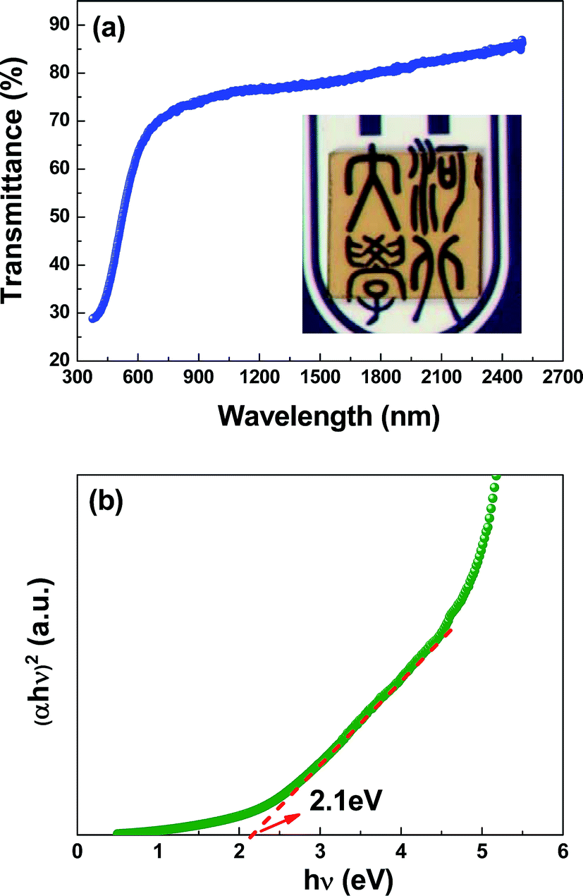 | ||
| Fig. 5 (a) The transmittance spectra of a 50 nm-thick Ca3Co4O9 thin film after abstracting the substrate contribution. The inset is the photography of this Ca3Co4O9 thin film on a labeled paper; (b) (αhν)2 versus hν plot of Ca3Co4O9 thin film. | ||
To evaluate the transparent conducting performance of the c-axis oriented Ca3Co4O9 thin films, we calculated the figure of merit FOM according to the equation of FOM = −1/(Rsh × lnT). It should be mentioned here that although both optical transmission T and sheet resistance Rsh of a TCO film increase with decreasing the film thickness d as expressed by T = e−αd and Rsh = 1/(σd), the FOM value (FOM = σ/α) of the film almost does not depend on the film thickness (assuming fixed ρ and α).12,19 However, if the film is too thin (for this work, if the Ca3Co4O9 film thickness is decreased to about 30 nm), the electrical conductivity σ of the film will decrease strongly with the decrease of film thickness due to the surface scattering, leading to an obvious deterioration in the optoelectronic properties of the film.20 Detailed works on the relationship between the Ca3Co4O9 film thickness (microstructure, doping, etc.) and its optoelectronic properties are required in our future work. The FOM of the present 50 nm-thick c-axis oriented Ca3Co4O9 films is calculated to be as high as 988 MΩ−1, which is almost 6–7 times higher than that reported for the corresponding polycrystalline Ca3Co4O9 thin films and is comparable to state-of-the-art p-type TCOs reported so far in literatures.5–12,14
Conclusion
Single-phase, c-axis oriented Ca3Co4O9 thin films were fabricated by pulsed laser deposition on LaAlO3 substrate. The resulting Ca3Co4O9 films were smooth and dense with very good crystalline quality. The room temperature resistivity of the films is about 7.3 mΩ cm and the average optical transmittance in the visible range of about 50%. A very high figure of merit (FOM) of 998 MΩ−1 was achieved in the c-axis oriented Ca3Co4O9 thin film, which is comparable to the best values reported for other p-type TCOs. This work opens up new strategy toward the practical applications of Ca3Co4O9 films as a promising p-type TCO coatings.Acknowledgements
This work was supported by the National Natural Science foundation of China (no. 51372064), the Nature Science Foundation of Hebei Province, China (nos A2013201249, A2014201176, QN20131040).References
- J. Lewis, S. Grego, B. Chalamala, E. Vick and D. Temple, Appl. Phys. Lett., 2004, 85, 3450 CrossRef CAS PubMed.
- K. Ellmer, Nat. Photonics, 2012, 6, 809 CrossRef CAS.
- K. Fleischer, E. Arca and I. V. Shvets, Sol. Energy Mater. Sol. Cells, 2012, 101, 262 CrossRef CAS PubMed.
- G. Hautier, A. Miglio, G. Ceder, G. M. Rignanese and X. Gonze, Nat. Commun., 2013, 4, 2292 Search PubMed.
- H. Kawazoe, M. Yasukawa, H. Hyodo, M. Kurita, H. Yanagi and H. Hosono, Nature, 1997, 389, 939–942 CrossRef CAS PubMed.
- H. M. Luo, M. K. Jain, T. M. McCleskey, E. Bauer, A. K. Burrell and Q. X. Jia, Adv. Mater., 2007, 19, 3604–3607 CrossRef CAS.
- M. J. Han, K. Jiang, J. Z. Zhang, W. L. Yu, Y. W. Li, Z. G. Hu and J. H. Chu, J. Mater. Chem., 2012, 22, 18463–18470 RSC.
- R. Bywalez, S. Götzendörfer and P. Löbmann, J. Mater. Chem., 2010, 20, 6562–6570 RSC.
- P. F. Zhai, Q. H. Yi, J. Jian, H. Y. Wang, P. Y. Song, C. Dong, X. Lu, Y. H. Sun, J. Zhao, X. Dai, Y. H. Lou, H. Yang and G. F. Zou, Chem. Commun., 2014, 50, 1854 RSC.
- E. Arca, K. Fleischer and I. V. Shvets, Appl. Phys. Lett., 2011, 99, 111910 CrossRef PubMed.
- H.-Y. Chen, H.-C. Su, C.-H. Chen, K.-L. Liu, C.-M. Tsai, S.-J. Yen and T.-R. Yew, J. Mater. Chem., 2011, 21, 5745–5752 RSC.
- M. Aksit, S. K. Kolli, I. M. Slauch and R. D. Robinson, Appl. Phys. Lett., 2014, 104, 161901 CrossRef PubMed.
- K. Koumoto, I. Terasaki and R. Funahashi, MRS Bull., 2006, 31, 206–210 CrossRef CAS.
- R. H. Wei, X. W. Tang, L. Hu, Z. Z. Hui, J. Yang, H. M. Luo, X. Luo, J. M. Dai, W. H. Song, Z. R. Yang, X. B. Zhu and Y. P. Sun, Chem. Commun., 2014, 50, 1854–1856 RSC.
- T. Takeuchi, T. Kondo, T. Takami, H. Takahashi, H. Ikuta, U. Mizutani, R. Funahashi, M. Shikano, M. Mikami, S. Tsuda, T. Yokoya, S. Shin and T. Muro, Phys. Rev. B: Condens. Matter Mater. Phys., 2004, 69, 125410 CrossRef.
- H. Z. Guo, S. F. Wang, L. Wang, K. J. Jin, S. S. Chen, G. S. Fu, C. Ge, H. B. Lu, C. Wang, M. He and G. Z. Yang, J. Appl. Phys., 2013, 113, 113707 CrossRef PubMed.
- A. C. Masset, C. Michel, A. Maignan, M. Hervieu, O. Toulemonde, F. Studer, B. Raveau and J. Hejtmanek, Phys. Rev. B: Condens. Matter Mater. Phys., 2000, 62, 166 CrossRef CAS.
- K. Agilandeswari and A. Ruban Kumar, J. Magn. Magn. Mater., 2014, 364, 117–124 CrossRef CAS PubMed.
- G. J. Exarhos and X. D. Zhou, Thin Solid Films, 2007, 515, 7025–7052 CrossRef CAS PubMed.
- J. Ravichandran, A. K. Yadav, W. Siemons, M. A. McGuire, V. Wu, A. Vailionis, A. Majumdar and R. Ramesh, Phys. Rev. B: Condens. Matter Mater. Phys., 2012, 85, 085112 CrossRef.
Footnote |
| † Electronic supplementary information (ESI) available. See DOI: 10.1039/c4ra16187d |
| This journal is © The Royal Society of Chemistry 2015 |