
Degradation mechanism of P3HT:PCBM-based bulk heterojunction solar cells†
Tirukoti
Mounika
a,
Manshi
Singh
b,
Inderpreet
Singh
 *b,
P.
Arun
b and
Kuldeep
Kumar
*c
*b,
P.
Arun
b and
Kuldeep
Kumar
*c
aEnvironmental Chemistry Laboratory, Department of Studies in Environmental Science, University of Mysore, Manasagangothri, Mysore, Karnataka 570006, India
bDepartment of Electronics, S.G.T.B. Khalsa College, University of Delhi, Delhi 110007, India. E-mail: inderpreetsingh_05@rediffmail.com
cDepartment of Physics, S.G.T.B. Khalsa College, University of Delhi, Delhi 110007, India. E-mail: kuldeep@sgtbkhalsa.du.ac.in; Tel: +91-8826076455
First published on 23rd April 2025
Abstract
We have studied the degradation mechanism of P3HT:PCBM-based bulk heterojunction solar cells by developing the structure ITO/PEDOT:PSS/P3HT:PCBM/Al comprising different acceptor materials, namely, PC60BM and PC70BM. Both the devices have nearly the same photoconversion efficiency (PCE) of ≈3.8% immediately after fabrication. The PCE is observed to decrease in both the devices with the passage of time. While the degradation rate is found to be higher in PC60BM based devices, its value is found to saturate after 100 minutes at a constant value of ≈2%. For PC70BM based cells, the devices show a sudden change in the degradation rate from low to high as the time progresses beyond ≈170 minutes. The PCE in these devices fell to a very low value after 250 minutes. This rapid fall in PCE is attributed to the formation of trap states in the energy levels of PC70BM molecules owing to their non-spherical structure.
Introduction
Bulk heterojunction solar cells based on polymers are becoming more popular because of their light weight, flexibility and ease of fabrication.1–5 Bulk heterojunctions are obtained using two materials, namely, donor and acceptor materials. The donor molecules, simply conjugated polymers, when exposed to sunlight produce excitons. The acceptor molecules break these excitons and drag the electrons towards themselves from the donor molecules due to their high electron affinity. The holes left inside the polymer chains travel towards the anode electrode, while the electrons that the acceptors collect hop towards the cathode electrode. Thus, the formation of a homogeneous bulk heterojunction where the donor and acceptor molecules are phase segregated at a nanometric scale is of utmost importance for achieving high photoconversion efficiency (PCE). The morphology of the bulk heterojunction interface has a major impact on exciton formation through light absorption and further on the dissociation of these excitons and transportation of free charge carriers6,7 to their respective electrodes.In the past two decades, researchers have made numerous efforts to design highly efficient bulk heterojunction photovoltaic devices.4,5,8–13 Different solar cell structures comprising diverse materials have been developed to achieve a high PCE. The strategies to improve the PCE include (i) selection of high performance donor–acceptor materials, their solvents, carrier transport layers and electrodes; (ii) optimizing the thickness of the photoactive layer, buffer layers and annealing parameters and (iii) designing inverted and/or tandem device structures.14–24 This has resulted in the development of photovoltaic devices with PCEs above 15%.23–29
Although organic solar cells have demonstrated the ability to create extremely effective devices, their low stability continues to be a bottleneck in their commercialization. The PCE of these photovoltaic devices decreases rapidly as soon as they come into contact with the atmospheric oxygen and water molecules.30,31 Therefore, it is difficult to achieve long-term stability in polymer-based solar cells. Encapsulating solar cell structures has been shown to shield them from ambient moisture, but there are a number of additional factors that affect the efficient working of the device. These are (a) separation of donor and acceptor molecules into individual phases,32,33 which destroys the bulk heterojunction. This in turn disrupts the dissociation of photogenerated excitons into individual charge carriers. (b) Diffusion of electrode atoms into the active layer.34,35 The presence of electrode atoms within the device structure disrupts the bulk heterojunction and film quality. (c) Photoinduced degradation, both polymer and acceptor molecules have the tendency to change their structure under illumination. For example, the PC60BM molecules can undergo dimerization (two molecules bonding together) in the presence of light.36,37 (d) Although individually the donor and acceptor molecules have a higher decomposition temperature, the morphology of the bulk heterojunction and individual participating layers requires an optimum working temperature. Higher temperatures lead to a poor morphology, thus deteriorating the device performance.38 All these factors act together and contribute to the deterioration of the device performance.
In the current study, we analyzed the performance and degradation of solar cell structures using PC60BM and PC70BM as acceptor materials and examined the reason for the gradual decline in the efficiency of P3HT:PCBM solar cells.
Experimental
All the chemicals required for the fabrication of the solar cells, namely, P3HT, PEDOT:PSS, PC60BM and PC70BM, were procured from Merck (USA). To prepare a composite solution, P3HT was dissolved in chlorobenzene maintaining the concentration at 10 mg ml−1. The mixture was then ultrasonically agitated for ≈2 hours to obtain a uniform solution. After that, 10 mg of PC60BM was dissolved in it, maintaining a 1![[thin space (1/6-em)]](https://www.rsc.org/images/entities/char_2009.gif) :1 P3HT:PC60BM ratio, and the mixture was once again ultrasonically agitated for ≈4 hours. Likewise, a 1:1 solution of P3HT and PC70BM was made in chlorobenzene. Both these solutions were used for the fabrication of solar cell structures. For device fabrication, an ITO coated glass substrate was taken and it was patterned using HCl to obtain fine electrodes. The width of ITO electrodes was kept at 0.4 cm. The patterned substrate was then cleaned (using DI water, isopropanol and acetone), and subsequently a layer of PEDOT:PSS was spin coated on top of it to serve as a hole transport layer. The substrates were then dried in an oven at 100 °C. Afterwards, a P3HT:PCBM solution was spin coated over it, and the so-obtained samples were again annealed at 120 °C for 10 minutes.
:1 P3HT:PC60BM ratio, and the mixture was once again ultrasonically agitated for ≈4 hours. Likewise, a 1:1 solution of P3HT and PC70BM was made in chlorobenzene. Both these solutions were used for the fabrication of solar cell structures. For device fabrication, an ITO coated glass substrate was taken and it was patterned using HCl to obtain fine electrodes. The width of ITO electrodes was kept at 0.4 cm. The patterned substrate was then cleaned (using DI water, isopropanol and acetone), and subsequently a layer of PEDOT:PSS was spin coated on top of it to serve as a hole transport layer. The substrates were then dried in an oven at 100 °C. Afterwards, a P3HT:PCBM solution was spin coated over it, and the so-obtained samples were again annealed at 120 °C for 10 minutes.
Finally, cathode electrodes of Al were coated over the composite film using the vacuum evaporation technique, keeping the electrode width at 0.2 cm. In this manner, a single substrate containing four solar cells each with an area of 0.4 × 0.2 cm2 was fabricated. Using this technique, batches of two different solar cell structures were prepared, ITO/PEDOT:PSS/P3HT:PC60BM/Al (which we shall henceforth refer to as device A) and ITO/PEDOT:PSS/P3HT:PC70BM/Al (device B), with ITO being the positive electrode and Al being the cathode electrode. Fig. 1 shows the cross-sectional view of a typical cell that we fabricated. The I–V characteristics of these photovoltaic devices were studied using a Keysight source-meter (Model B2910BL) by illuminating the cells from the ITO side using a 300 W Osram light source. The intensity of light on solar cells was measured using a lux meter and was observed to be 46000 lux. The input power (PIN) from the sun lamp to solar cells was calculated to be 6.73 mW cm−2.
 | ||
| Fig. 1 The typical cross-sectional view of the solar cell fabricated in this study (layer thicknesses shown are not to scale). | ||
Results and discussion
Fig. 2 displays the J–V characteristics of typical solar cells fabricated with PC60BM and PC70BM. Under illumination, both the devices display J–V curves in the fourth quadrant, which represent photovoltaic activity in our samples. We discovered that the efficiency of the devices immediately after fabrication was the same (within experimental error) regardless of whether they were fabricated using PC60BM or PC70BM. The I–V characteristics in the logarithmic scale are also shown in the figure. Important characterising parameters of these cells are listed in Table 1.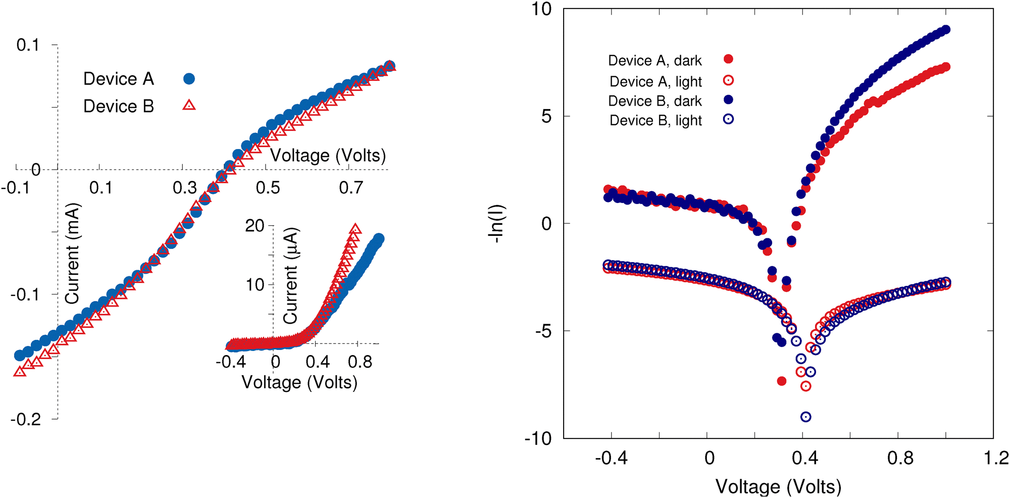 | ||
| Fig. 2 Comparison of the I–V characteristics of device A and device B, with the inset showing the IV characteristics of the same devices measured in the dark. The efficiency of the two devices immediately after fabrication is approximately equal. The second panel shows the same in the logarithmic scale. | ||
| Device | V co (V) | I sc (mA) | J sc (mA cm−2) | P max (mVA cm−2) | FF | PCE (%) |
|---|---|---|---|---|---|---|
| A | 0.41 | 0.13 | 1.61 | 0.21 | 0.31 | 3.16 |
| B | 0.43 | 0.14 | 1.73 | 0.21 | 0.28 | 3.16 |
To understand the solar cells' deterioration with time, the J–V curves were examined at regular intervals (of 30–40 minutes). The devices were kept in the dark between the two measurements. Fig. 3 displays the change in PCE of the solar cell structures over time for both devices ‘A’ and ‘B’. The graph shows how the solar cells’ PCE declines with time. Since a slight change in fabrication conditions could result in a change in PCE due to the randomness in the bulk heterojunction production, we have produced up to four cells in a batch to take this into consideration. The PCE variations of these cells’ fall inside the colour band. The solid line represents the average change over time for all the cells. The exponentially falling trend in device performance is evident (which saturates after t > 100 minutes for device A). Data points of all the four cells showed similar variations, and hence for brevity the area in which the points lay have been shown as a shaded region.
 | ||
| Fig. 3 PCE variation of as many as four cells of device A and device B with time is found to lie within the color bands. The exponential line within shows the variation of the average. | ||
The degradation in PCE for both the devices is observed to follow exponential variation with time, which can be mathematically given as
| η (in%) = Aexp(−αt) + B. | (1) |
The decay in PCE was rapid in device A (α = 0.026 min−1) until t = 100 minutes after which it saturates at about ≈2%. Compared to this, the decay in the PCE of device B is slower with α = 0.007 min−1. However, beyond 170–180 minutes, the deterioration rate distinctly increases and α becomes 0.012 min−1. Though we were not able to unambiguously prove this, there is a possibility that α for PC70BM varies with time.
Duan38et al. also observed such an exponential fall in the PCE of their solar cells. They ascribed this “burn in” to the aggregation of fullerene molecules via dimerizations, which alters the morphology of the bulk heterojunction interface,39–43 resulting in a decrease in efficiency. Dimerization is also accompanied by breaking of bonds formed between dangling bonds of P3HT and PCBM.44 This light assisted dimerization, hence, creates traps causing deterioration of the device.45 Furthermore, in our earlier study on PC60BM cells,46 we were able to explain the deterioration in PCE based on the study by Berriman et al.47, which showed post PC60BM segregation from P3HT to form large aggregates (dimerization) that diffused towards the surface of the films. The SEM micrograph in Fig. 4 confirmed this idea. The delayed deterioration of device B can be explained due to the PC70BM molecule's asymmetrical (ellipsoid) shape, which prevents the bond faces of fullerene molecules from aligning as needed for cyclo-addition,39–43 and due to large inertia arising on account of their heavier mass.
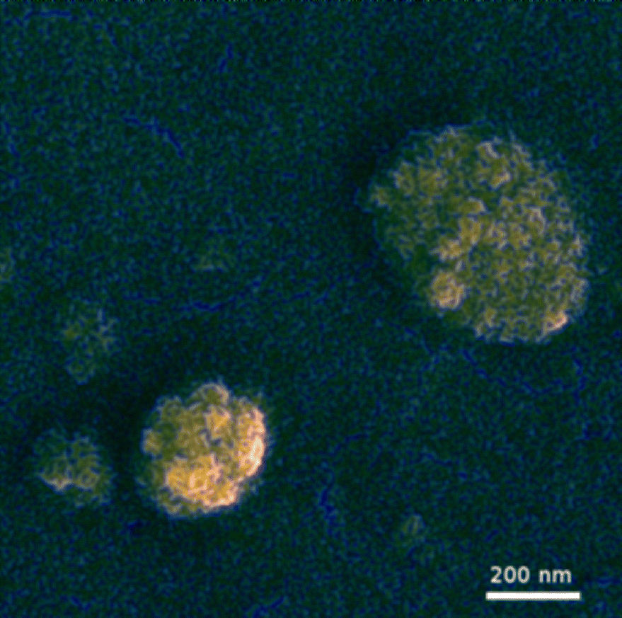 | ||
| Fig. 4 The micrograph shows clusters of PC60BM molecules wrapped in thread-like P3HT polymer structures. Some of these clusters are seen to be present within the film and a few are above the film surface, as can be appreciated by shadow formation. This validates the conclusion drawn by Berriman et al.47 that the P3HT and PCBM molecules tend to move away from each other forming distinct individual domains. The PCBM clusters then move towards the surface. | ||
The rapid degradation of device B after 170–180 minutes (absent in device A) is due to oxidation of PC70BM molecules that have reached the surface and are exposed to air. The spherical symmetry of PC60BM ensures that it has an inert behavior and a reluctance to react with oxygen, while the ellipsoidal shape of PC70BM results in strains within the molecule which results in bond breaking and sites for reaction with oxygen. This oxidation results in new energy levels appearing near the band edges, which contribute to deep traps. These traps have the capability of capturing free charge carriers, thus hindering their movement in the photoactive layer. Again, in our previous study on PC60BM,46 we experimentally showed that traps were absent in our samples (device A) and hence deterioration was not related to oxidation. The deterioration was due to phase separation of P3HT and PC60BM, on account of dimerization and movement of PC60BM towards the film surface.
To prove the influence of traps on our device's PCE,48 we have calculated the ideality factor (h) for both the devices at different intervals of time using the I–V data. The degree to which a device's current–voltage (I–V) characteristics adhere to the ideal diode equation is measured using the ideality factor. An ideality factor of 2 (two) would imply the disappearance of charge carriers by electron–hole pair's recombination in a perfect-defectless crystal lattice. It is well established that an ideality factor greater than two (2) in the diode equation indicates traps/defects in the junction. The ideality factor was determined using the method listed in the literature.49,50 The diode equation is given as
 | (2) |
The terms in the above equation have their usual meaning. On taking the logarithm on both sides of the above equation, we get an equation of a line from which η is easily computed from the slope. We have computed the values of η using the linear part of the curve for V > 0 (Fig. 2, second panel). The values of η obtained using both the methods were found to be similar. The variation in the ideality factor with time for both the devices is shown in Fig. 5. It can be observed that under dark conditions the value of the ideality factor for both the devices remains at ≈2, thus indicating a nearly perfect diode behavior free of defect states. However, under illumination, the values of the ideality factor increase, indicating either the activation of the deep traps or their creation as described above.
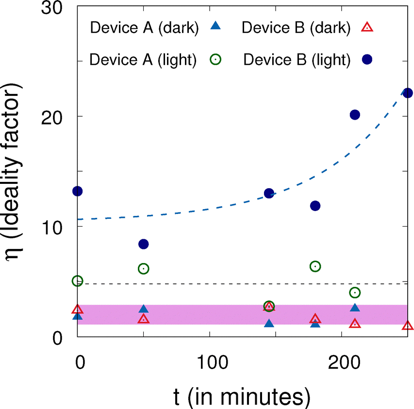 | ||
| Fig. 5 The ideality factor of the two devices measured in the dark and light shows that oxidation in the presence of light distinguishes the performance of device B from that of device A. | ||
The ideality factor of device A when exposed to light was observed to be constant throughout the time period of investigation (∼6). This is interesting since this constant in the ideality factor seems to result in constant α, the decay rate of eqn (1) which was a constant throughout the time period of study for device A. On the other hand, the value of the ideality factor for device B is found to be large (∼11) which kept on increasing after 180 minutes of device fabrication (to a maximum value of ∼22) depicting the presence of deep traps, which would have been created as PC70BM reacted with oxygen at the surface. The increase in deep traps in the photoactive layer leads to a reduction in device current and efficiency.
To emphasise the role of traps (through the ideality factor), in Fig. 6 we show the variation in the PCE of device B as a function of the ideality factor. The device's efficiency falls off exponentially with the increase in the value of the ideality factor. A similar trend was reported for CdS/SnS junctions.50 For completeness, the energy level diagram of our structure is shown in Fig. 7. The figure shows the ease with which holes move towards the ITO anode and electrons towards the Al cathode due to the appropriate energy levels. The trap levels, generated (reflected by the increasing ideality factor), appear within the bandgap and prove to be detrimental to the flow of charge carriers to their respective electrodes. Hence this impediment is represented by a series resistance in the solar cell. Remember, an increase in series resistance distorts the solar cell's I–V properties. As a result, the solar cell's ideality factor and series resistance are related. Series resistance increases in tandem with an increase in the ideality factor in solar cells, reducing the cells’ efficiency.
 | ||
| Fig. 6 The rapid decrease in the solar cell efficiency (device B) with its ideality factor proves that defects are detrimental to the device's performance. | ||
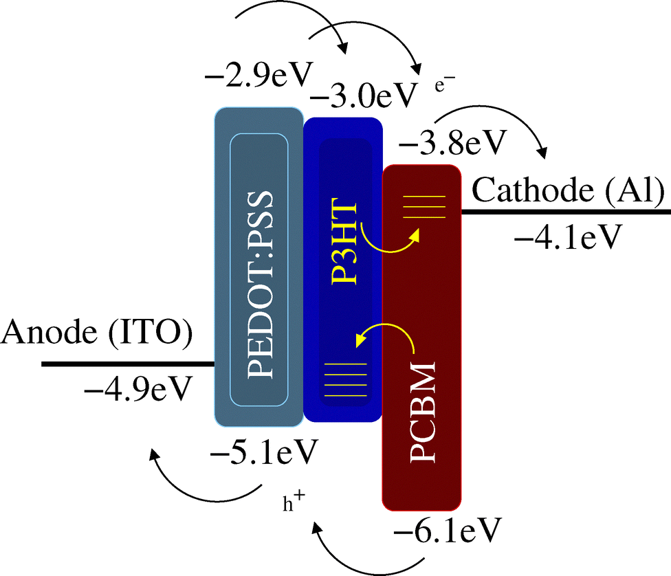 | ||
| Fig. 7 The energy level diagram shows how positioning of energy levels of P3HT:PCBM helps in the movement of holes (h+) and electrons (e−) to their respective electrodes. The appearance of trap levels within the bandgap, however, prevents easy and fast movement of carriers towards the electrode. | ||
Conclusion
The bulk heterojunction not only promotes exciton transfer and charge separation, but also helps in passivation of traps present in buckyball structures, which may be present in the form of dangling bonds. With time, the PC60BM molecules owing to their symmetric structure tend to dimerize and initiate phase separation in the photoactive layer. This deteriorates the PCE of device A. Conversely, PC70BM molecules owing to their ellipsoid shape agglomerate at a slower rate, and thus, phase separation in the photoactive layer in device B is slower. The deterioration in these devices is not as fast as that in device A. With passage of time, the agglomeration continues in the active layer, and the fullerene structures move away from the polymer molecules towards the surface. Deep traps are created in the PC70BM molecules due to their reaction with oxygen at the surface. As PC70BM molecules develop traps, the PCE deteriorates at a faster rate than before.Data availability
The data that support this article have been included as part of the ESI.†Conflicts of interest
There are no conflicts to declare.Acknowledgements
The authors gratefully acknowledge the financial assistance given by the R & D Center, S.G.T.B. Khalsa College (SGTBKC/2689).References
- L. Duan, N. K. Elumalai, Y. Zhang and A. Uddin, Sol. Energy Mater. Sol. Cells, 2019, 193, 22 CrossRef CAS
.
- C. Yan,
et al.
, Nat. Rev. Mater., 2018, 3, 18003 CrossRef CAS
- A. Wadsworth,
et al.
, Chem. Soc. Rev., 2019, 48, 1596 RSC
- K. K. Sadasivuni,
et al.
, J. Mater. Sci.: Mater. Electron., 2019, 30, 951 CrossRef CAS
- J. Bergqvist,
et al.
, npj Flexible Electron., 2018, 2, 4 CrossRef
- B. Ray, P. R. Nair and M. A. Alam, Sol. Energy Mater. Sol. Cells, 2011, 95, 3287 CrossRef CAS
- W. Ma,
et al.
, Adv. Funct. Mater., 2005, 15, 1617 CrossRef CAS
- D. Koo,
et al.
, Joule, 2020, 4, 1021 CrossRef CAS
- I. Singh,
et al.
, J. Nanophotonics, 2011, 5, 053504 CrossRef
- Z. Wang,
et al.
, Adv. Funct. Mater., 2021, 31, 2103534 CrossRef CAS
- S. Chen,
et al.
, Adv. Energy Mater., 2018, 8, 1800529 CrossRef
- Y. A. Mohammed, F. A. Hone, G. T. Mola and N. A. Tegegne, Phys. B, 2023, 653, 414666 CrossRef CAS
- R. Sondergaard,
et al.
, Mater. Today, 2012, 15, 36 CrossRef CAS
- J. Hou, O. Inganas, R. H. Friend and F. Gao, Nat. Mater., 2018, 17, 119 CrossRef CAS
- R. S. Gurney, D. G. Lidzey and T. Wang, Rep. Prog. Phys., 2019, 82, 036601 CrossRef CAS
- C. Xu,
et al.
, Org. Electron., 2018, 62, 261 CrossRef CAS
- Y. Zhang,
et al.
, Adv. Mater., 2018, 30, 1707508 CrossRef
- L. Duan,
et al.
, Mater. Sci. Semicond. Process., 2020, 105, 104750 CrossRef CAS
- R. Sun,
et al.
, Energy Environ. Sci., 2019, 12, 384 RSC
- C. Xie,
et al.
, ACS Appl. Mater. Interfaces, 2018, 10, 23225 CrossRef CAS PubMed
- J. Zhang,
et al.
, Nat. Energy, 2018, 3, 720 CrossRef CAS
- B. Fan,
et al.
, Sci. China Chem., 2019, 62, 746 CrossRef CAS
- J. Yuan,
et al.
, Joule, 2019, 3, 1140 CrossRef CAS
- L. Hong,
et al.
, Adv. Mater., 2018, 31, 1903441 CrossRef
- T. Lei,
et al.
, Mater. Today Energy, 2019, 14, 100334 CrossRef
- Q. Liu,
et al.
, Sci. Bull., 2020, 65, 272 CrossRef CAS
- B. Fan,
et al.
, Sci. China Chem., 2019, 62, 746 CrossRef CAS
- L. Meng,
et al.
, Science, 2018, 361, 1094 CrossRef CAS PubMed
- Y. Lin,
et al.
, Adv. Mater., 2019, 31, 1902965 CrossRef CAS
- A. Perthue,
et al.
, J. Mater. Res., 2018, 33, 1868 CrossRef CAS
- V. Blazinic,
et al.
, Phys. Chem. Chem. Phys., 2019, 21, 22259 RSC
- S. Alam,
et al.
, J. Photonics Energy, 2022, 12, 035501 CAS
- A. Y. Ali,
et al.
, Coatings, 2023, 13, 1293 CrossRef CAS
- K. Feron,
et al.
, Sol. Energy Mater. Sol. Cells, 2013, 109, 169 CrossRef CAS
- E. Voroshazi,
et al.
, ACS Appl. Mater. Interfaces, 2015, 7, 618 CrossRef CAS
- I. Ramirez,
et al.
, Nat. Commun., 2021, 12, 471 CrossRef CAS PubMed
- M. Causa,
et al.
, J. Phys. Chem. Lett., 2018, 9, 1885 CrossRef CAS
- L. Duan and A. Uddin, Adv. Sci., 2020, 7, 1903259 CrossRef CAS
- T. Heumueller,
et al.
, Adv. Energy Mater., 2015, 5, 1500111 CrossRef
- M. B. Upama,
et al.
, Nanoscale, 2017, 9, 18788 RSC
- L. Duan,
et al.
, Mater. Chem. Front., 2019, 3, 1085 RSC
- N. Wang,
et al.
, Energy Environ. Sci., 2015, 8, 1005 RSC
- Q. C. Burlingam,
et al.
, Energy Environ. Sci., 2015, 8, 1005 RSC
- Y. Finck and J. Schwartz, Phys. Rev. Appl., 2016, 6, 054008 CrossRef
- S. Cowan, A. Roy and A. Heeger, Phys. Rev. B: Condens. Matter Mater. Phys., 2010, 82, 245207 CrossRef
- T. Mounika,
et al.
, Appl. Sol. Energy, 2023, 59, 410 CrossRef
- G. A. Berriman,
et al.
, Org. Electron., 2016, 30, 12 CrossRef CAS
- A. Foertig,
et al.
, Phys. Rev. B: Condens. Matter Mater. Phys., 2012, 86, 115302 CrossRef
- Y. Gupta and P. Arun, J. Active Passive Electron. Devices, 2019, 14, 1 Search PubMed
- Y. Gupta, C. Ravikant and P. Arun, Global Challenges, 2020, 1, 1800017 Search PubMed
Footnote |
| † Electronic supplementary information (ESI) available. See DOI: https://doi.org/10.1039/d5sm00024f |
| This journal is © The Royal Society of Chemistry 2025 |