
 Open Access Article
 This Open Access Article is licensed under a
 Creative Commons Attribution 3.0 Unported Licence
Nanostructured amorphous gallium phosphide on silica for nonlinear and ultrafast nanophotonics†
Benjamin
Tilmann
 *a,
Gustavo
Grinblat
b,
Rodrigo
Berté
a,
Mehmet
Özcan
c,
Viktoria F.
Kunzelmann
d,
Bert
Nickel
c,
Ian D.
Sharp
d,
Emiliano
Cortés
a,
Stefan A.
Maier
ae and
Yi
Li
*af
*a,
Gustavo
Grinblat
b,
Rodrigo
Berté
a,
Mehmet
Özcan
c,
Viktoria F.
Kunzelmann
d,
Bert
Nickel
c,
Ian D.
Sharp
d,
Emiliano
Cortés
a,
Stefan A.
Maier
ae and
Yi
Li
*af
aChair in Hybrid Nanosystems, Nanoinstitut München, Fakultät für Physik, Ludwig-Maximilians-Universität München, 80539 München, Germany. E-mail: b.tilmann@physik.uni-muenchen.de
bDepartamento de Física, FCEN, IFIBA-CONICET, Universidad de Buenos Aires, C1428EGA Buenos Aires, Argentina
cFakultät für Physik and Center for NanoScience (CeNS), Ludwig-Maximilians-Universität, 80539 München, Germany
dWalter Schottky Institut and Physics Department, Technische Universität München, Am Coulombwall 4, 85748 Garching, Germany
eThe Blackett Laboratory, Department of Physics, Imperial College London, London SW7 2AZ, UK
fSchool of Microelectronics, MOE Engineering Research Center of Integrated Circuits for Next Generation Communications, Southern University of Science and Technology, Shenzhen 518055, China. E-mail: liy37@sustech.edu.cn
First published on 30th September 2020
Abstract
Nanophotonics based on high refractive index dielectrics relies on appreciable contrast between the indices of designed nanostructures and their immediate surrounding, which can be achieved by the growth of thin films on low-index substrates. Here we propose the use of high index amorphous gallium phosphide (a-GaP), fabricated by radio-frequency sputter deposition, on top of a low refractive index glass substrate and thoroughly examine its nanophotonic properties. Spectral ellipsometry of the amorphous material demonstrates the optical properties to be considerably close to crystalline gallium phosphide (c-GaP), with low-loss transparency for wavelengths longer than 650 nm. When nanostructured into nanopatches, the second harmonic (SH) response of an individual a-GaP patch is characterized to be more than two orders of magnitude larger than the as-deposited unstructured film, with an anapole-like resonant behavior. Numerical simulations are in good agreement with the experimental results over a large spectral and geometrical range. Furthermore, by studying individual a-GaP nanopatches through non-degenerate pump–probe spectroscopy with sub-10 fs pulses, we find a more than 5% ultrafast modulation of the reflectivity that is accompanied by a slower decaying free carrier contribution, caused by absorption. Our investigations reveal a potential for a-GaP as an adequate inexpensive and CMOS-compatible material for nonlinear nanophotonic applications as well as for photocatalysis.
New conceptsIn the search for new and promising dielectrics for nonlinear nanophotonics, the refractive index contrast between the material and the surrounding medium is arguably next to loss the most important aspect, as it enables judicious modal design of the cavity response. In this work we propose the deposition of amorphous gallium phosphide thin films at a CMOS compatible temperature and demonstrate linear and nonlinear optical properties that are comparable to that of crystalline structure of the material. We measure a nonzero and only marginally smaller SHG than from the bulk crystal and we can resonantly enhance SHG by more than two orders than magnitude via nanostructuring. Further investigations with sub-10 fs pulses reveal an ultrafast modulation of the reflectivity by more than 5% with a slow decaying free carrier contribution that is caused by absorption. This is a significant difference to the reported, pure ultrafast response of crystalline GaP and suggests the amorphous variant as a promising candidate for photocatalytic applications on the nanoscale. Altogether, our investigations reveal a new alternative to crystalline GaP that eliminates disadvantages of on-wafer fabrication techniques by being inexpensive, easy and flexible to deposit on any substrate of choice. |
Introduction
In recent years, all-dielectric nanostructures have been shown to outperform well-studied and understood plasmonic nanoparticles in a number of nanophotonic applications.1,2 In particular in the optical regime – the visible and near infrared (IR) region of the electromagnetic spectrum – semiconductors exhibit a transparency that is only limited by the spectral position of their electronic bandgap wavelength, while metals show strong Ohmic losses and absorption due to the presence of free carriers at all wavelengths. For nonlinear optics, this effectively restricts the optically active region mainly to the surface while Mie-like resonances in dielectric structures can spread the field over the entire volume.3 This property has already been employed to successfully explore second4–8 and third9–11 harmonic generation as well as frequency mixing12,13 with dielectric nanoparticles, exceeding the achieved efficiencies of comparable plasmonic systems. Furthermore, the lack of linear absorption reduces photon–electron interactions and thus promotes all-dielectric structures as a platform for non-destructive all-optical switching, sensing and data processing,14–19 in particular at high powers above the damage threshold of plasmonic metals.Most of these studies are based on the excitation of electromagnetic resonant modes that confine the electric and/or magnetic fields in dielectric nano-resonators, thus boosting the intrinsically low efficiency of nonlinear effects.20 To achieve this, a strong refractive index contrast between the dielectric material and the surrounding medium is needed, leading to a research focus on high refractive index materials such as AlGaAs,7,21–23 Ge9,10,24 and Si.8,15,17 Among this class of materials, one of the most promising is gallium phosphide (GaP), with previously reported efficient second harmonic generation (SHG),4,25–27 all-optical switching14 and integrated waveguides,28 capable of covering almost the entire visible range with negligible losses. However, the investigated GaP nanostructures were mostly limited to expensive on-wafer fabrication techniques leading to an identical high refractive index substrate, and thus restricting the optical contrast in one direction.
In this work, we demonstrate the deposition and nanostructuring of a high refractive index film of amorphous GaP on top of a low refractive index glass substrate at a CMOS compatible temperature (∼250 °C) and characterize its intrinsic and resonant nonlinear optical response using SHG and ultrafast pump–probe spectroscopy. We analyze the dependence of the nonlinear signals on the incident polarization and perform numerical simulations that are in good agreement with our experimental findings. Our studies suggest sputtered amorphous GaP as a promising and flexible candidate for nonlinear and ultrafast nanophotonics, which comprises the low-cost and the high-accessibility high-performance beyond conventional c-GaP on-wafer techniques.
Results and discussion
A GaP film was first sputtered on top of a glass substrate, followed by two dry etching steps to define dielectric nanopatches of different sizes using gold and silicon dioxide as hard masks. The desired design was transferred to the sample using a standard electron beam lithography (EBL) procedure with PMMA as photoresist (refer to Methods for fabrication details). To characterize the composition of the as-deposited, uncapped film, we performed X-ray photoelectron spectroscopy (XPS) measurements, with the Ga 2p and P 2p core level peaks shown in Fig. 1a and b, respectively (green lines). As a reference, a commercial double side polished wafer of intrinsic c-GaP (Institute of Electronic Materials Technology, Warsaw) was used, shown in red. The measurements exhibit nearly identical features and are in very good agreement with each other and with literature values.29,30 Due to the presence of a low energy satellite feature in the P 2p region (Fig. 1b), direct quantitative analysis of the Ga![[thin space (1/6-em)]](https://www.rsc.org/images/entities/char_2009.gif) :P elemental ratio was not possible. To overcome this, the intensity ratio of the Ga–P components from the Ga 2p3/2 region to the P 2p region was compared between the sputtered film and reference sample, which possesses a known stoichiometric composition. The intensity ratio for the a-GaP is within 5% of that from the c-GaP wafer which is near the error limits of this method, thus confirming that the deposited material is stoichiometric GaP. Furthermore, the XPS survey spectra (ESI†) from the c-GaP reference and the sputtered a-GaP film are nearly identical, with no additional impurity elements observed for the sputtered material. To further prove the amorphous structure of the sputtered film, we performed X-ray diffraction (XRD) and compared it again to the [100] oriented wafer, shown in Fig. 1c. As expected, the latter exhibits clear peaks in the diffraction pattern that correspond to the (200) and (400) orientations, in excellent agreement with literature values.31,32 In contrast, the a-GaP film shows a weaker and broad response without any clear feature or pronounced peak. Such pattern can be attributed to an amorphous structure without long-range order.33 The full XRD patterns of wafer and film can be found in the ESI.† Further, to study the optical quality of the amorphous film, we investigated its linear optical properties through spectral ellipsometry. We determined the complex permittivity ε, with real and imaginary parts shown in Fig. 1d and e (green curves), respectively, and compared it to the results of the crystalline wafer (red curves). In good agreement with band structure calculations,34 the c-GaP sample has an imaginary part of ε that is only nonzero for wavelengths shorter than the direct bandgap at 450 nm while being effectively lossless for the remaining extent of the spectrum. In the case of the amorphous film, the absorption edge is red-shifted towards 650 nm, which can be explained by increased impurity-assisted electron transitions in the defect-rich amorphous structure. Nevertheless, the sputtered a-GaP is transparent for part of the visible and all of the near IR spectrum with an extinction coefficient that is lower than that for other common semiconductors such as Ge or GaAs (a comparison of the materials can be found in the ESI†). The measured difference in the optical constants between the a-GaP film and the c-GaP wafer results in a darker orange appearance of the former, visible in the optical image in the inset of Fig. 1d. However, the determined values of the real part of ε are close to c-GaP for most of the investigated spectral range (500 nm–1.5 μm), leading to a refractive index n′ = √Re(ε) larger than 3.
:P elemental ratio was not possible. To overcome this, the intensity ratio of the Ga–P components from the Ga 2p3/2 region to the P 2p region was compared between the sputtered film and reference sample, which possesses a known stoichiometric composition. The intensity ratio for the a-GaP is within 5% of that from the c-GaP wafer which is near the error limits of this method, thus confirming that the deposited material is stoichiometric GaP. Furthermore, the XPS survey spectra (ESI†) from the c-GaP reference and the sputtered a-GaP film are nearly identical, with no additional impurity elements observed for the sputtered material. To further prove the amorphous structure of the sputtered film, we performed X-ray diffraction (XRD) and compared it again to the [100] oriented wafer, shown in Fig. 1c. As expected, the latter exhibits clear peaks in the diffraction pattern that correspond to the (200) and (400) orientations, in excellent agreement with literature values.31,32 In contrast, the a-GaP film shows a weaker and broad response without any clear feature or pronounced peak. Such pattern can be attributed to an amorphous structure without long-range order.33 The full XRD patterns of wafer and film can be found in the ESI.† Further, to study the optical quality of the amorphous film, we investigated its linear optical properties through spectral ellipsometry. We determined the complex permittivity ε, with real and imaginary parts shown in Fig. 1d and e (green curves), respectively, and compared it to the results of the crystalline wafer (red curves). In good agreement with band structure calculations,34 the c-GaP sample has an imaginary part of ε that is only nonzero for wavelengths shorter than the direct bandgap at 450 nm while being effectively lossless for the remaining extent of the spectrum. In the case of the amorphous film, the absorption edge is red-shifted towards 650 nm, which can be explained by increased impurity-assisted electron transitions in the defect-rich amorphous structure. Nevertheless, the sputtered a-GaP is transparent for part of the visible and all of the near IR spectrum with an extinction coefficient that is lower than that for other common semiconductors such as Ge or GaAs (a comparison of the materials can be found in the ESI†). The measured difference in the optical constants between the a-GaP film and the c-GaP wafer results in a darker orange appearance of the former, visible in the optical image in the inset of Fig. 1d. However, the determined values of the real part of ε are close to c-GaP for most of the investigated spectral range (500 nm–1.5 μm), leading to a refractive index n′ = √Re(ε) larger than 3.
 | ||
| Fig. 1 High resolution XPS measurement of (a) the Ga 2p3/2 region and (b) the P 2p peak for the as deposited a-GaP film (green) and the c-GaP wafer (red). The black dashed line represents a peak fitting with the background shown by the brown solid line. (c) XRD measurements of the [100] c-GaP wafer (red) and a-GaP film (red). The wafer shows a crystalline pattern with the (200) and (400) orientations indicated. (d) and (e) Ellipsometry data of the c-GaP wafer (red) and the a-GaP film (green), with (d) the real and (e) the imaginary part of the dielectric function ε. Inset: Optical image of the c-GaP wafer and the a-GaP film, taken under identical illumination. | ||
Next, we investigated the second-order response of the a-GaP film through SHG measurements at a pump wavelength of 1120 nm (see Methods for nonlinear characterization specifics). As shown in Fig. 2a, a second harmonic response at the expected wavelength of 560 nm is observed for the a-GaP film (green curve). Comparing the magnitude of the signal to a reference measurement with the c-GaP wafer (red curve) indicates an effective second-order susceptibility χ(2) that is smaller for the amorphous film by a factor <2. As shown in Fig. 2b, this trend is confirmed over a wide range of excitation power densities of 0–102 μW mm−2. A linear fit in double logarithmic scale leads to the expected slopes close to 2, confirming the second-order nature of the process.
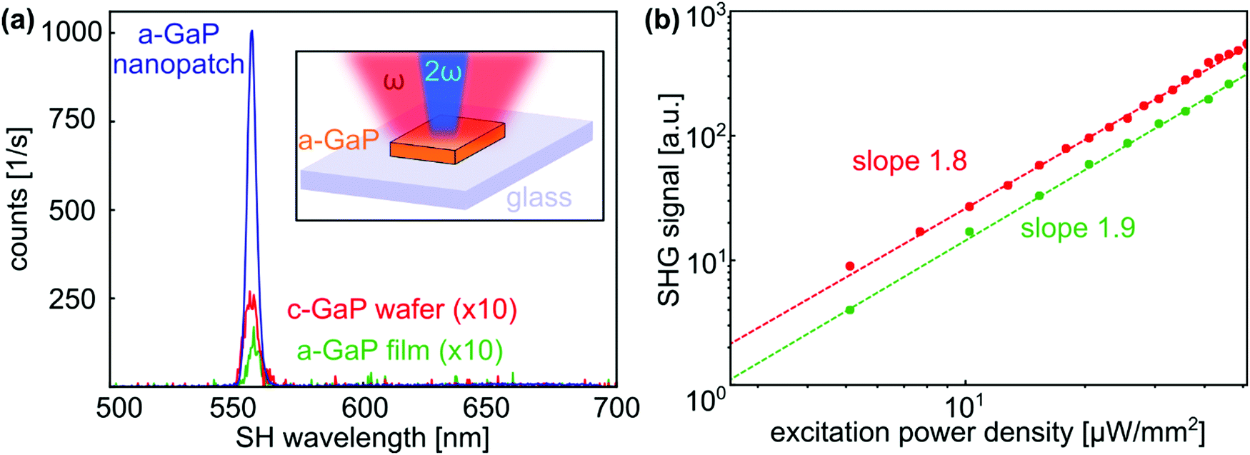 | ||
| Fig. 2 (a) Spectral SHG response at a fundamental wavelength of 1120 nm and 10.2 μW mm−2 average pump power for the c-GaP wafer (red), a-GaP film (green) and a single a-GaP nanopatch (blue). Inset: Sketch of the SHG measurement of a GaP nanopatch on glass substrate. (b) Power dependence for the c-GaP wafer and a-GaP film at double logarithmic scale. The dashed lines represent a fitting to a linear model resulting in the indicated slopes. | ||
To enhance the nonlinear response of the as-deposited a-GaP film, an array of etched nanopatches with a fixed height of 260 nm was investigated. A scanning electron microscope (SEM) image of the fabricated structures is shown in Fig. 3a, where patches with widths and lengths varying from 100 nm to 1000 nm can be observed (see ESI† for more details on the fabricated array). In particular, the SHG signals from two patches with dimensions of 675 nm × 375 nm and 900 nm × 450 nm, in the following referred as patch 1 and patch 2, respectively, were measured individually. Remarkably, a comparison of patch 1 with the bare film at a pump wavelength of 1120 nm results in an enhancement of the SHG signal by more than two orders of magnitude, as it can be seen in Fig. 2a. This is about one order of magnitude lower than for c-Gap, where SHG enhancement by more than three orders of magnitude by nanostructuring was reported.4 Reasons for this discrepancy could be the difference in the nonlinear susceptibility χ(2) or SHG self-absorption, which naturally limits the SHG emission. Further, we studied the second harmonic response of the two nanopatches over a spectral excitation range of 1000–1400 nm at a constant pump power density of 10.2 μW mm−2. This leads to clear SHG peaks for 1120 nm and 1250 nm excitation wavelength for patch 1 and patch 2, respectively, as shown in Fig. 3b (top panels). To gain a better understanding of this resonant behavior, numerical simulations were carried out, using the finite difference time domain (FDTD) method (see Methods for simulation details). We started by calculating the square of the normalized electric energy stored inside the nanoantenna WV2, defined by 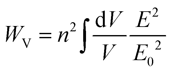 (see bottom panels in Fig. 3b), with V being the volume of the nanopatch. As SHG depends on the square of the incident light intensity, WV2 can be regarded as the effective excitation power of the conversion process. In Fig. 3b we can see a very good agreement between the calculated curve and the experimentally measured spectral dependence of SHG. The deviation of the peak widths can be attributed to the conversion process itself and emission directionality which were not considered in the numerical analysis. Further simulations including a multipole decomposition, as shown in Fig. 3c and d, reveal that the observed peaks in the electric energy are accompanied by a dip in the total scattering (black curves), leading to the respective electric and magnetic field distributions included in Fig. 3b. Such a behavior can be attributed to non-radiating, anapole-like excitations in the nanopatches, that are known to strongly enhance the electric energy.35,36
 | ||
| Fig. 3 (a) SEM image of the fabricated a-GaP nanopatch array. The red arrow indicates the pump polarization of the SHG measurements. Scale bar: 10 μm. Inset: Single 1000 nm × 1000 nm patch, tilted by 45°. Scale bar: 200 nm. (b) Experimental spectral SHG response for patch 1 and patch 2 (top) and corresponding numerical WV2 values (bottom). The inset shows the fundamental near field distribution of the electric (E) and magnetic (H) field for the respective maximum wavelengths indicated. Multipole decomposition for (c) patch 1 and (d) patch 2. Included are the first three orders, namely electric/magnetic dipole (ED/MD), quadrupole (EQ/MQ) and octupole (EO/MO). The black solid line represents the simulated total scattering cross section. The dashed lines mark the wavelengths showing maximum SHG. | ||
To verify our findings on a larger scale, the SHG signal of the entire nanopatch array (accounting for a total of 1369 nanoantennas) was monitored at a pump wavelength of 1120 nm, with the resulting SHG map shown in Fig. 4a. As expected, the generated signal depends strongly on the nanopatch dimensions, with the strongest signal occurring around the location of patch 1.
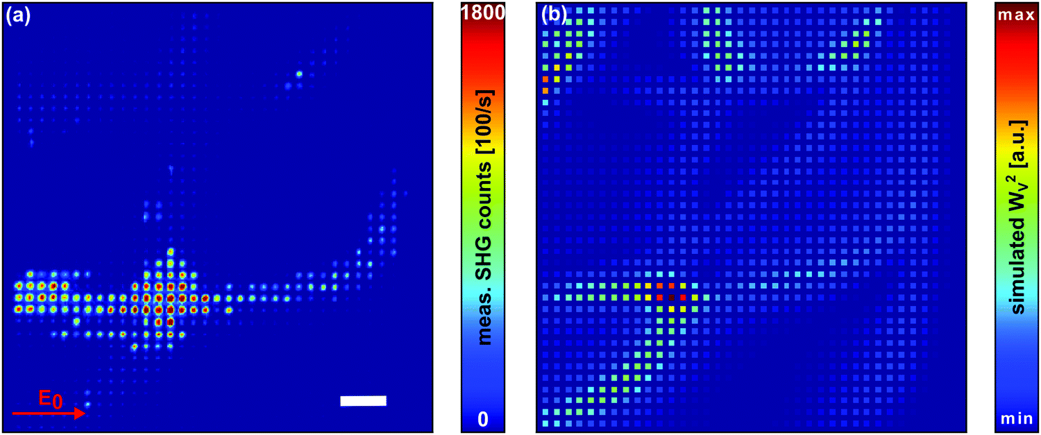 | ||
| Fig. 4 (a) SHG measurement of the entire nanopatch array from Fig. 2a. The fundamental wavelength is 1120 nm with an average excitation power of 25.5 μW mm−2. The red arrow indicates the pump polarization. Scale bar: 10 μm. (b) Numerical simulation of the square of the electric energy (WV2) for the array in (a). Each square represents the respective patch with dimensions corresponding to this position. | ||
Even more, we find that the orientation of the patches with respect to the incident polarization plays an important role. While specific antennas that are orientated parallel to the fundamental beam generate the strongest signal, their rotated counterparts appear as almost inert. This behavior is confirmed by a measurement of the same array, but with opposite (vertical) polarization (see ESI†), where all features appear at the corresponding mirrored positions. As for the single patches in Fig. 3, the simulation of WV2 in Fig. 4b shows a good agreement with the measured SHG signal over a large region of the nanopatch array. Especially close to the position of patch 1, computational results and experiment are in very good agreement, with numerical calculations accurately describing most features visible in the measurement, even for the smallest patches. The observed small deviations between experiment and theory can be attributed to effects such as emission directionality or SHG self-absorption, which were not considered in the calculations. The fact that the latter scales with the volume of the nanopatches, explains the greater deviation for larger structures. To ensure the reproducibility at a different wavelength, an identical measurement for a pump wavelength of 1020 nm can be found in the ESI.† As expected for a shorter wavelength, the strongest responses appear shifted towards smaller antennas, also in good agreement with the corresponding simulations.
We now turn our attention to the ultrafast response of the sputtered GaP nanopatches, characterized through nondegenerate pump–probe spectroscopy using sub-10 fs laser pulses in the 600–1000 nm wavelength range (refer to Methods for experimental details). Fig. 5a shows the measured differential reflectivity −ΔR/R for a square patch pumped (probed) with a 750–1000 nm (600–750 nm) wavelength beam. At the temporal pump–probe overlap position (t = 0 fs), the nanoantenna exhibits a maximum differential reflectivity value of 5.6% at a probe wavelength of 690 nm, which decreases towards shorter wavelengths. Over the measured spectral range, the response is dominated by a slow decaying modulation that is commonly attributed to free carriers,37 excited by two-photon absorption. However, for a probe wavelength around 675 nm, this slow component is overwhelmed by a sharp response at precisely the overlap position t = 0 fs, as it can be seen in the temporal trace presented in Fig. 5d. Such an ultrafast response, separated from the slow component, is especially interesting for all-optical signal processing38 and was previously reported for c-GaP14,39 (a detailed comparison can be found in the ESI†). Comparing the performance of the patches with the as-deposited a-GaP film (black curve in Fig. 5d), shows that nanostructuring enhances the peak nonlinear signal by more than a factor of 5. Moreover, it should be stressed that an ultrafast response of this magnitude is larger than reported for perovskite single crystals37 or Au-clad Si discs.40 We further note that a measurement with exchanged pump and probe beams (see ESI†) shows no pronounced ultrafast peak, given that free carrier absorption is dominant when pumping with the short-wavelength beam.
 | ||
| Fig. 5 Differential reflectivity −ΔR/R contour plots with respect to the probe wavelength and the pump–probe delay time for three patches with dimensions (a) 625 nm × 625 nm, (b) 625 nm × 850 and (c) 850 nm × 625 nm. The dashed lines mark the 675 nm probe wavelength that is shown in temporal traces (d)–(f) for the respective patches. Red solid lines represent fittings to the convolution of exponential rise/decay and the IRF for the ultrafast response and exponential decay for the slow decaying part, respectively. The resulting time constants are indicated. The response of the as-deposited a-GaP film is shown in black. | ||
To exploit the observed polarization dependence of the sample, identical measurements were performed on two orthogonally oriented rectangular patches of identical size, as shown in Fig. 5b and c. To simplify the analysis, Fig. 5d–f shows the temporal traces results taken from Fig. 5a–c, respectively, at the specific probe wavelength of 675 nm. A maximum value for the differential reflectivity of 5.6% is observed for the squared antenna (Fig. 5a and d) that is reached after a rising time of 20.5 fs, computed by fitting of a convolution between an exponential and a Gaussian function, with the latter being the approximation of the instrument response function (IRF) of our system.14 To fit the relaxation dynamics of the signal, two exponential decay functions are needed, again a convolution with the IRF for the ultrafast component and a single one for the slow part, respectively. We find that there is a fast decay time of 12.8 fs which can be attributed to a combination of the nonlinear Kerr effect and two-photon absorption14,37,40 combined with a slow relaxation component of 3.8 ps, product of the free carrier contribution, which is comparable to other amorphous semiconductors.41 When comparing the squared nanoantenna (Fig. 5a) with the elongated nanopatches (Fig. 5b and c), we find that the response of all three nanostructures show the same features, differing only in the magnitude of the differential reflectivity. While the patch that is orientated parallel to the incident polarization reaches slightly higher values than the square patch, the rotated antenna reduces the modulation depth by more than 40%. The same behavior can be observed in the evaluation of the reference temporal traces at λ = 675 nm, shown in Fig. 5d–f. Nevertheless, it should be noted that even for the perpendicular elongated patch (Fig. 5e) the peak response is larger than that of the as-deposited film by a factor of 3.
Conclusion
In summary, thin films of GaP were fabricated using radio frequency sputter deposition, resulting in an amorphous material with optical constants close to the bulk crystalline counterpart. Nanostructuring of the film further improved the SHG signal by more than two orders of magnitude with numerical simulations that are in good agreement over a wide range of the nanopatch dimensions and for different excitation wavelengths. Pump–probe measurements of the nanostructures revealed a strong nonlinear and ultrafast response that decays within <100 fs, accompanied by a smaller slow-decaying feature attributed to free carrier contributions, at a probe wavelength of 675 nm. For both, SHG and ultrafast responses, a strong dependence of the signal and the orientation of the nanopatch with respect to the fundamental beam polarization was observed. Even though the sputtered film has no well-defined crystal structure, the achieved nonlinear responses are close to previously reported values for c-GaP,4,14 proposing a-GaP as a promising inexpensive and flexible material with excellent optical properties. Moreover, its considerable absorption in the solar spectrum and the observed carrier dynamics make it an exciting candidate for other areas such as photocatalysis at the nanoscale with confined photocarrier transport, as reported for dielectric TiO2−x nano-resonators.42Methods
Sample fabrication
The films were fabricated using radio frequency sputter deposition with a 3 inch GaP target in an Angstrom deposition tool. The procedure was carried out at a constant rate of 1 Å s−1 while the glass substrate was constantly heated to 250 °C. After cooling down, the same tool was used to deposit a capping layer of SiO2, again via sputter deposition. Before the procedure, a standard microscopy borosilicate cover glass substrate was cleaned, using acetone and isopropanol (IPA). As a positive photoresist, PMMA was deposited on top using spin coating. The EBL was carried out with an exposure dose of 400 mC cm−2 with a 10 μm aperture and external high voltage (EHT) of 20 kV. After the development for 30 s in MIBK:IPA and 30 s in IPA, gold as a hard mask was deposited using thermal evaporation. A lift-off procedure was carried out by a bath in acetone for 4 h. In a first inductively coupled plasma reactive ion etching (ICP-RIE) dry etching step, the mask was etched into the silica layer with CHF6 (20 sccm) and Ar (30 sccm) as processing gases. Afterwards the gold was removed by rinsing the sample in Au-etchant for a few seconds. Finally, again ICP-RIE with Cl2 (10 sccm) and Ar (30 sccm) as processing gases was used to transfer the nanostructures into the GaP film.Sample characterization
The XPS measurements were recorded with a homebuilt setup using an Al X-ray source and a pass energy Epass = 25 eV. The energetic positions of all spectra were calibrated using the adventitious carbon by shifting the C–C bond position in the C 1s core level spectrum to 284.8 eV. The spectra were fitted to Voigt type line shapes after a Shirley or linear background correction (software CasaXPS). The X-ray source could be switched to Mg, allowing to differentiate Auger and core level XPS peaks for the later analysis. The XRD measuements were recorded at LMU using the rotating crystal method.43 A monochromatic Mo Kα (λ = 0.71073 Å) beam from a sealed tube is selected by a parabolic mulilayer monochromator white line focus, i.e., the X-ray beam is highly collimated in horizontal direction and rather divergent in the vertical. At the sample position the beam cross-section is 10 × 0.35 mm2. The GaP samples were aligned with their surface normal along the horizontal direction and rotated slowly with constant angular velocity, while the diffracted intensities were recorded by a Dectric Pilatus 100k area detector. The system was calibrated with a standard powder sample measurement under the same conditions (Lanthanum hexaboride).The ellipsometry measurements were done with a Variable Angle Spectroscopic Ellipsometry (VASE) instrument from J. A. Woollam over the visible to near-IR spectral range.
SHG experiments
The used laser systems comprises a Yb:KGW Pharos 1030 nm pump laser with a repetition rate of 200 kHz that pumps a collinear optical parametric amplifier (OPA) Orpheus-HP (both by Light Conversion Ltd). The OPA converts the IR beam to a selectable wavelength between 300 nm and 3 μm with an average output power of ∼1 W and a pulse duration of ∼180 fs. The beam was sent to a microscope with a 100×/Numerical Aperture (NA) = 0.9 objective that focused the beam on the sample, which was mounted on a XYZ – piezo stage. The generated light was then collected with the same objective and a rotatable mirror sent it either to an avalanche photo diode (APD) or a spectrometer. By scanning over the sample and measuring the collected SHG signal in each point, SHG maps as Fig. 4a could be recorded.Pump–probe experiments
The same laser system was set to a wavelength of 1120 nm to pump a 5 mm thick sapphire plate with an average power of 600 mW to generate 3 mW of supercontinuum (SC) light. A sketch of the pump–probe setup, including the generated SC spectrum can be found in the ESI.† This light was then sent to multiphoton intrapulse interference phase scan device (MIIPSBox640-P by Biophotonic Solutions Inc.) that allows to compress the pulses in time to below 10 fs FWHM at the sample position. Dichroic beam splitters were used to divide the spectrum into two 600–750 nm and 750–1000 nm independent beams. A motorized delay line allowed to control the temporal offset between pump and probe pulses with accuracy below 1 fs. To reduce dispersion effects, low group velocity dispersion (GVD) mirrors and a dispersion free metal objective with NA = 0.5 were used to direct and focus the beams. The reflected probe beam was then sent to a spectrograph coupled with a low-noise Si photodiode by FEMTO. Lock-in detection was used by modulating the pump beam using an optical chopper operating at frequencies below 1 kHz. The IRF of the system is described by a Gaussian function with a full-width half-maximum of 11 fs, that approximates the convolution of pump and probe beam. More details on the experimental pump–probe setup can be found published elsewhere.14Numerical simulation
The numerical simulations were performed with the commercially available software Lumerical FDTD. A plane wave total-field scattered-field (TFSF) was used to facilitate the evaluation of the scattering problem. The simulation region was restricted by perfectly matched layer boundaries to imitate antennas in an infinite space. The experimental data of the ellipsometry measurements of the sputtered GaP film as well as for the bare coverglass were used as input for the materials dielectric function in the simulation. The multipole decomposition and calculation of the near field distribution were carried out using the commercially available finite-element method solver COMSOL Multiphysics with the RF module. The multipole analysis follows the procedure published by COMSOL and is based on the equations of Mie theory. It makes use of the expansion in means multipole coefficients, using the scattering current that is source of the scattering field.44Conflicts of interest
There are no conflicts to declare.Acknowledgements
This work was funded by the Deutsche Forschungsgemeinschaft (DFG, German Research Foundation) under Germany's Excellence Strategy, EXC 2089/1-390776260, and the Bavarian programme Solar Energies Go Hybrid (SolTech). We also acknowledge the support of the Center of Nanoscience (CENS). S. A. M. additionally acknowledges the EPSRC Reactive Plasmonics Programme (EP/M013812/1), the Leverhulme Trust and the Lee-Lucas Chair in Physics, and E. C. acknowledges the ERC Starting Grant 802989 CATALIGHT. G. G. and E. C. acknowledge support by PICT grant No. 2017-2534. Y. L. acknowledges the funding received from the Natural Science Foundation of Guandong Province (2019A1515111136) as well as the European Union's Framework Programme for Research and Innovation Horizon 2020 (2014–2020) under the Marie Skłodowska-Curie Grant Agreement No. 754388 (LMU Research Fellows) and from LMUexcellent as part of LMU Munich's funding as University of Excellence within the framework of the German Excellence Strategy.References
- A. I. Kuznetsov, A. E. Miroshnichenko, M. L. Brongersma, Y. S. Kivshar and B. Luk’yanchuk, Optically resonant dielectric nanostructures, Science, 2016, 354, aag2472 Search PubMed.
- G. Brönstrup, et al., Optical properties of individual silicon nanowires for photonic devices, ACS Nano, 2010, 4, 7113–7122 Search PubMed.
- K. Koshelev, et al., Subwavelength dielectric resonators for nonlinear nanophotonics, Science, 2020, 367, 288–292 Search PubMed.
- J. Cambiasso, et al., Bridging the gap between dielectric nanophotonics and the visible regime with effectively lossless gallium phosphide antennas, Nano Lett., 2017, 17, 1219–1225 Search PubMed.
- L. Carletti, K. Koshelev, C. De Angelis and Y. Kivshar, Giant Nonlinear Response at the Nanoscale Driven by Bound States in the Continuum, Phys. Rev. Lett., 2018, 121, 033903 Search PubMed.
- P. P. Vabishchevich, et al., Enhanced second-harmonic generation using broken symmetry III–V semiconductor fano metasurfaces, ACS Photonics, 2018, 5, 1685–1690 Search PubMed.
- L. Carletti, A. Locatelli, O. Stepanenko, G. Leo and C. De Angelis, Enhanced second-harmonic generation from magnetic resonance in AlGaAs nanoantennas, Opt. Express, 2015, 23, 26544–26550 Search PubMed.
- S. V. Makarov, et al., Efficient second-harmonic generation in nanocrystalline silicon nanoparticles, Nano Lett., 2017, 17, 3047–3053 Search PubMed.
- G. Grinblat, Y. Li, M. P. Nielsen, R. F. Oulton and S. A. Maier, Enhanced third harmonic generation in single germanium nanodisks excited at the anapole mode, Nano Lett., 2016, 16, 4635–4640 Search PubMed.
- G. Grinblat, Y. Li, M. P. Nielsen, R. F. Oulton and S. A. Maier, Efficient Third Harmonic Generation and Nonlinear Subwavelength Imaging at a Higher-Order Anapole Mode in a Single Germanium Nanodisk, ACS Nano, 2017, 11, 953–960 Search PubMed.
- T. Shibanuma, G. Grinblat, P. Albella and S. A. Maier, Efficient third harmonic generation from metal-dielectric hybrid nanoantennas, Nano Lett., 2017, 17, 2647–2651 Search PubMed.
- S. Liu, et al., An all-dielectric metasurface as a broadband optical frequency mixer, Nat. Commun., 2018, 9, 2507 Search PubMed.
- X. Lu, et al., Efficient telecom-to-visible spectral translation through ultralow power nonlinear nanophotonics, Nat. Photonics, 2019, 13, 593–602 Search PubMed.
- G. Grinblat, et al., Ultrafast sub–30-fs all-optical switching based on gallium phosphide, Sci. Adv., 2019, 5, eaaw3262 Search PubMed.
- M. R. Shcherbakov, et al., Ultrafast All-Optical Switching with Magnetic Resonances in Nonlinear Dielectric Nanostructures, Nano Lett., 2015, 15, 6985–6990 Search PubMed.
- M. R. Shcherbakov, et al., Ultrafast all-optical tuning of direct-gap semiconductor metasurfaces, Nat. Commun., 2017, 8, 17 Search PubMed.
- G. Della Valle, et al., Nonlinear anisotropic dielectric metasurfaces for ultrafast nanophotonics, ACS Photonics, 2017, 4, 2129–2136 Search PubMed.
- J. Cambiasso, M. König, E. Cortés, S. Schlücker and S. A. Maier, Surface-Enhanced Spectroscopies of a Molecular Monolayer in an All-Dielectric Nanoantenna, ACS Photonics, 2018, 5, 1546–1557 Search PubMed.
- M. Caldarola, et al., Non-plasmonic nanoantennas for surface enhanced spectroscopies with ultra-low heat conversion, Nat. Commun., 2015, 6, 7915 Search PubMed.
- R. W. Boyd, Nonlinear Optics, Elsevir Academic Press, 2008, DOI:10.1016/B978-0-12-369470-6.00001-0.
- L. Ghirardini, et al., Shaping the nonlinear emission pattern of a dielectric nanoantenna by integrated holographic gratings, Nano Lett., 2018, 18, 6750–6755 Search PubMed.
- L. Carletti, A. Locatelli, D. Neshev and C. De Angelis, Shaping the radiation pattern of second-harmonic generation from AlGaAs dielectric nanoantennas, ACS Photonics, 2016, 3, 1500–1507 Search PubMed.
- L. Carletti, et al., Nonlinear goniometry by second harmonic generation in AlGaAs nanoantennas, ACS Photonics, 2018, 5, 4386–4392 Search PubMed.
- S. Campione, et al., Broken symmetry dielectric Resonators for high quality factor fano metasurfaces, ACS Photonics, 2016, 3, 2362–2367 Search PubMed.
- R. Sanatinia, S. Anand and M. Swillo, Modal engineering of second-harmonic generation in single GaP nanopillars, Nano Lett., 2014, 14, 5376–5381 Search PubMed.
- R. Sanatinia, S. Anand and M. Swillo, Experimental quantification of surface optical nonlinearity in GaP nanopillar waveguides, Opt. Express, 2015, 23, 756–764 Search PubMed.
- R. Sanatinia, M. Swillo and S. Anand, Surface second-harmonic generation from vertical GaP nanopillars, Nano Lett., 2012, 12, 820–826 Search PubMed.
- D. J. Wilson, et al., Integrated gallium phosphide nonlinear photonics, Nat. Photonics, 2020, 14, 57–62 Search PubMed.
- D. L. Cui, et al., Stability and surface reactivity of gallium phosphide nanocrystals, Prog. Cryst. Growth Charact. Mater., 2000, 40, 145–151 Search PubMed.
- J. L. Bourque, M. C. Biesinger and K. M. Baines, Chemical state determination of molecular gallium compounds using XPS, Dalton Trans., 2016, 45, 7678–7696 Search PubMed.
- K. Persson, Materials Data on GaP (SG:216) by Materials Project, DOI:10.17188/1200314.
- H. Emmer, et al., Fabrication of Single Crystal Gallium Phosphide Thin Films on Glass, Sci. Rep., 2017, 7, 2–7 Search PubMed.
- B. D. Cullity and S. R. Stock, Elements of X-Ray Diffraction. Plant Management & Physiology, 1978 Search PubMed.
- R. Zallen and W. Paul, Band structure of gallium phosphide from optical experiments at high pressure, Phys. Rev., 1964, 134, 1628–1641 Search PubMed.
- A. E. Miroshnichenko, et al., Nonradiating anapole modes in dielectric nanoparticles, Nat. Commun., 2015, 6, 1–8 Search PubMed.
- R. Paniagua-Domínguez, B. Luk’yanchuk, A. Miroshnichenko and J. A. Sánchez-Gil, Dielectric nanoresonators and metamaterials, J. Appl. Phys., 2019, 126, 150401 Search PubMed.
- G. Grinblat, et al., Ultrafast All-Optical Modulation in 2D Hybrid Perovskites, ACS Nano, 2019, 13, 9504–9510 Search PubMed.
- M. Z. Alam, S. A. Schulz, J. Upham, I. De Leon and R. W. Boyd, Large optical nonlinearity of nanoantennas coupled to an epsilon-near-zero material, Nat. Photonics, 2018, 12, 79–83 Search PubMed.
- G. Grinblat, et al., Efficient ultrafast all-optical modulation in a nonlinear crystalline gallium phosphide nanodisk at the anapole excitation, Sci. Adv., 2020, 6, eabb3123 Search PubMed.
- G. Grinblat, et al., Sub-20 fs All-Optical Switching in a Single Au-Clad Si Nanodisk, Nano Lett., 2018, 18, 7896–7900 Search PubMed.
- S. Kumar, et al., Probing ultrafast carrier dynamics, nonlinear absorption and refraction in core-shell silicon nanowires, Pramana – J. Phys., 2012, 79, 471–481 Search PubMed.
- L. Hüttenhofer, et al., Anapole Excitations in Oxygen-Vacancy-Rich TiO2−x Nanoresonators: Tuning the Absorption for Photocatalysis in the Visible Spectrum, ACS Nano, 2020, 14, 2456–2464 Search PubMed.
- B. E. Warren, X-ray diffraction, Dover Publications, 1990 Search PubMed.
- P. Grahn, A. Shevchenko and M. Kaivola, Electromagnetic multipole theory for optical nanomaterials, New J. Phys., 2012, 14, 093033 Search PubMed.
Footnote |
| † Electronic supplementary information (ESI) available. See DOI: 10.1039/d0nh00461h |
| This journal is © The Royal Society of Chemistry 2020 |