
Proposed mechanical method for switching the spin transport channel in two-dimensional magnetic metal–magnetic semiconductor van der Waals contacts†
Pengfei
Gao
,
Xingxing
Li
 * and
Jinlong
Yang
*
* and
Jinlong
Yang
*
Department of Chemical Physics, Hefei National Laboratory for Physical Sciences at the Microscale, and Synergetic Innovation Center of Quantum Information & Quantum Physics, University of Science and Technology of China, Hefei, Anhui 230026, China. E-mail: lixx@ustc.edu.cn; jlyang@ustc.edu.cn
First published on 18th August 2020
Abstract
Developing simple nonmagnetic methods to efficiently control spin transport across magnetic metal–magnetic semiconductor contacts plays a key role in developing high-performance nano-spintronic devices, since a magnetic field is hard to apply locally. For this purpose, based on first principles calculations, we here propose a mechanical means for manipulating the spin transport across two-dimensional magnetic metal–magnetic semiconductor van der Waals contacts formed between representative metallic Fe3GeTe2 and semiconducting CrGeTe3/CrI3 nanosheets. For such contacts, there exist four spin resolved Schottky barriers, i.e. the n/p-type Schottky barriers in the up/down spin channels, in which the dominant transport spin channel, characterized by the lowest Schottky barrier, can be selectively switched by regulating the magnetic coupling between the magnetic metal and magnetic semiconductor via interfacial sliding. In this way, single spin channel ohmic contacts with reversible spin polarization have been realized.
New conceptsA new basic physical picture for two-dimensional magnetic metal–magnetic semiconductor contacts inherent to nano-spintronic devices and an efficient simple mechanical method for controlling the spin transport across such contacts have been demonstrated. While previous studies are mostly focused on modulating the electron transport properties of nonmagnetic metal–semiconductor contacts, such as achieving ohmic conductivity, the properties of magnetic metal–magnetic semiconductor contacts and their controllability have been largely overlooked, which are however very crucial to the development of high-performance nano-spintronic devices. For example, developing simple nonmagnetic methods to control spin transport across such contacts for efficient spin injection and manipulation is urgently needed, since a conventional magnetic field is hard to apply locally and becomes unrealistic with the device size miniaturized to the nanometer/sub-nanometer scale. Here we propose a mechanical means to selectively switch between spin up and spin down electron/hole transport channels by regulating the magnetic coupling between the magnetic metal and magnetic semiconductor via interfacial sliding. Through this method, a novel class of contacts named single spin channel ohmic contacts with reversible spin polarization have been realized. The developed spin control method will accelerate the design of good performance nanoscale magnetic contacts and guide the realization of high-performance spintronic devices. |
In spintronics, magnetic metal–magnetic semiconductor contacts, inherently formed when magnetic semiconductors are integrated with magnetic metal electrodes, are crucial in determining the device performance.1–4 To control spin transport across such contacts for efficient spin injection and manipulation is one of the key scientific issues in spintronics. To achieve this goal, an external magnetic field is generally required to separately and precisely modulate the magnetic states of the metal and semiconductor, which however becomes more and more challenging when the device size is continuously miniaturized to the nanometer/sub-nanometer scale. Therefore, developing other simple alternative methods to efficiently control spin transport across magnetic metal–magnetic semiconductor contacts is urgently needed.5
In this paper, we propose such a method based on van der Waals (vdW) contacts formed by two-dimensional (2D) magnetic metal Fe3GeTe2 and 2D magnetic semiconductors CrGeTe3/CrI3, which have been recently synthesized in experiments.6–8 Let us first recall the nonmagnetic metal–semiconductor contacts that widely exist in microelectronics, in which, due to the different electrochemical potentials between the metal and semiconductor, Schottky barriers will emerge (Fig. 1a), namely hole and electron Schottky barriers (ϕBp, ϕBn). Although sometimes a finite Schottky barrier is useful for making electrical elements such as Schottky diodes, in most cases, a zero Schottky barrier, i.e. ohmic contacts, between the metal and semiconductor is highly desirable. Previous studies have suggested that vdW contacts between 2D nonmagnetic metals and semiconductors with saturated surfaces are able to reduce the Fermi level pining effect and help to obtain ohmic conductance.9,10 When the spin degree of freedom is incorporated into such contacts, a natural question occurs: is it possible to realize an ohmic contact for a certain spin channel or even is the transport spin channel controllable?
 | ||
| Fig. 1 Schematic diagram of the electronic structure for (a) a 2D nonmagnetic metal–semiconductor vdW contact with two Schottky barriers (ϕBp, ϕBn), and 2D magnetic metal–magnetic semiconductor vdW contacts with (b) ferromagnetic and (c) antiferromagnetic interlayer coupling, which present four spin resolved Schottky barriers (ϕupBp, ϕdownBp, ϕupBn, ϕdownBn). ‘M’ stands for the macroscopic magnetization with the direction indicated by black arrows (the magnetization is just a sketch map and can be in any direction in reality). The green lines represent the projected bands (PBANDS) for the semiconductor, while the gray lines represent the PBANDS of the metal. The red and blue colors indicate up and down spin, respectively. (d) and (e) show the spin switching process of the 2D magnetic metal–magnetic semiconductor vdW contact via interfacial sliding. | ||
Here, through theoretical studies of 2D magnetic metal–magnetic semiconductor vdW contacts between Fe3GeTe2 and CrGeTe3/CrI3, we propose that in such contacts, not only ohmic conductance for specific spin channels is achievable, but also the transport spin channel can be switched. The underlying mechanism is simple: different from nonmagnetic contacts where only two Schottky barriers exist, magnetic metal–magnetic semiconductor contacts possess four spin resolved Schottky barriers, i.e. the hole and electron Schottky barriers for the up spin (ϕupBp, ϕupBn) and down spin (ϕdownBp, ϕdownBn) channels (Fig. 1b), while the carriers will preferentially transmit through the spin channel with the lowest barrier. Since the electronic and magnetic interactions between the 2D vdW stacked magnetic metal and magnetic semiconductor are relatively weak and sensitive to external stimuli, the relative size of the four Schottky barriers and the transport spin channel can be in principle adjusted by introducing appropriate actions, such as stress induced interfacial sliding and electrical gating.
A typical situation is that the interlayer magnetic coupling changes from ferromagnetic (FM) to antiferromagnetic (AFM) under interfacial sliding. Fig. 1b and c show the four Schottky barriers at different interlayer magnetic states. In the FM coupled contact (Fig. 1b) where ϕupBn is defined to be the lowest barrier, the electrons in the up spin channel will dominate the conduction. When the interlayer magnetic coupling is tuned to AFM, ϕdownBn becomes the lowest barrier (Fig. 1c), and electrons in the down spin channel are conducted. In this manner, the transport spin channel of the 2D vdW contact can be selectively switched. Note that the interfacial sliding induced magnetic transitions have been confirmed in bilayer CrI3 both theoretically and experimentally.11,12Fig. 1d and e demonstrate how the spin switching device based on the 2D magnetic metal–magnetic semiconductor contact works: when an external force induces lateral sliding between the 2D magnetic metal and magnetic semiconductor, the interlayer magnetic coupling undergoes a FM–AFM transition, and accordingly the spin polarization direction of the current is reversed.
To validate the above proposal, taking the magnetic metal–magnetic semiconductor vdW contact Fe3GeTe2/CrGeTe3 as an example, the variations of the total energy and interlayer exchange energy (defined as the energy difference between the FM and AFM states) with respect to lateral sliding are scanned by first principles calculations, where the interlayer FM–AFM transition is identified between two nonequivalent metastable stacking patterns (named A/B stacking). Under A-stacking, in the AFM ground state, the contact is an ohmic contact for the down spin channel, while the ohmic spin channel switches to be up spin under FM coupled B-stacking. The sliding between A and B stacking is feasible with a small energy barrier (∼90 meV). Similar results are also observed in other experimentally accessible magnetic metal–magnetic semiconductor vdW contacts Fe3GeTe2/CrI3.
The Fe3GeTe2/CrGeTe3 contact is constructed by matching the unit cell of magnetic semiconductor CrGeTe3 to the ( ) supercell of magnetic metal Fe3GeTe2 with the lattice mismatch being about 3.4% (Fig. 2a). The optimized interlayer distance is around 3.2 Å and no chemical bonding occurs between Fe3GeTe2 and CrGeTe3, implying the formation of a vdW contact. The 2D interfacial sliding potential energy surface for Fe3GeTe2/CrGeTe3 with the interlayer magnetic coupling set as FM is displayed in Fig. 2b. The potential energy surface in the AFM state is similar, as shown in Fig. S1a in the ESI.† Two nonequivalent metastable stacking patterns, named A-stacking (red rectangle) and B-stacking (blue rectangle), are found, with A-stacking being only about 60 meV higher in energy than B-stacking. The two stacking patterns can be switched easily between each other by lateral sliding along the [010] or equivalent [100] direction of the superlattice, with a small energy barrier of about 90 meV (Fig. S1b, ESI†).
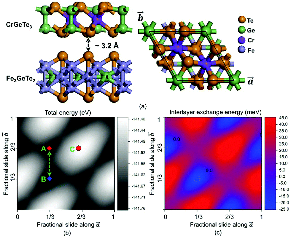 | ||
Fig. 2 (a) The structure of the Fe3GeTe2/CrGeTe3 contact from side (left panel) and top (right panel) views. (b) The lateral sliding potential energy surface of Fe3GeTe2/CrGeTe3 with FM interlayer coupling. The red and blue rectangles represent metastable A-stacking and B-stacking patterns, respectively. The red circle represents the highest energy stacking, which is a saddle point on the potential energy surface. (c) 2D map of the interlayer exchange energy (E(FM) − E(AFM) per supercell) as a function of fractional lateral slide. The abscissa and ordinate stand for the fractional shift of the CrGeTe3 layer in the ![[a with combining right harpoon above (vector)]](https://www.rsc.org/images/entities/i_char_0061_20d1.gif) and and ![[b with combining right harpoon above (vector)]](https://www.rsc.org/images/entities/i_char_0062_20d1.gif) directions of the superlattice, respectively. Red (positive values) and blue colors (negative values) indicate AFM and FM coupling, respectively. directions of the superlattice, respectively. Red (positive values) and blue colors (negative values) indicate AFM and FM coupling, respectively. | ||
To reveal the sliding dependent interlayer magnetic coupling, the 2D map of the interlayer exchange energy per supercell is given in Fig. 2c. It is clear that the interlayer magnetic coupling is quite sensitive to the interfacial sliding. In particular, the metastable A-stacking prefers AFM coupling, while B-stacking prefers FM coupling. Thus, a FM–AFM magnetic transition is expected when the A and B stacking are switched between each other via interfacial sliding. The origin of such a magnetic transition is different from the super-superexchange mechanism in bilayer CrI3 where the different dihedral angles along Cr–I–I–Cr exchange paths among metastable structures play a decisive role.11 In the A- and B-stacking Fe3GeTe2/CrGeTe3, the dihedral angles along Fe–Te–Te–Cr exchange paths are almost the same. Also, the quite small difference in the interlayer Te–Te distance between A- and B-stacking (∼0.03 Å) excludes the recently proposed interlayer distance dependent double super-exchange mechanism.13 Therefore, the origin of the interlayer magnetic transition in Fe3GeTe2/CrGeTe3 is believed to be more complicated than we expected, which needs further theoretical studies.
To investigate the electronic properties of the Fe3GeTe2/CrGeTe3 contact, and determine the Schottky barriers, the band structures projected onto CrGeTe3 (red circles for up spin, blue circles for down spin) are calculated for the AFM coupled A-stacking and FM coupled B-stacking patterns. From Fig. 3a, one can see that for A-stacking, the electron Schottky barrier in the down spin channel vanishes (ϕdownBn = 0), indicating an ohmic contact for down spin electrons, while significant electron and hole Schottky barriers exist in the up spin channel. For B-stacking (Fig. 3b), the ohmic contact is kept but changes into the up-spin channel (ϕupBn = 0). Therefore, when the contact is shifted from A-stacking to B-stacking, the spin direction of transmitted electrons will be reversed, which is consistent with our proposal.
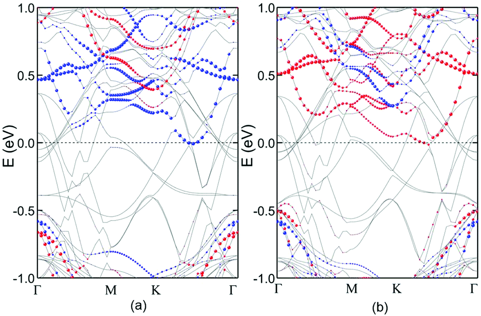 | ||
| Fig. 3 The electronic structure of the Fe3GeTe2/CrGeTe3 contact. (a) and (b) are the projected electronic bands of A-stacking and B-stacking, respectively. The gray lines represent the bands of the whole contact. The red (blue) circles represent the up (down) spin bands of magnetic semiconductor CrGeTe3. The Fermi levels are set to zero. | ||
Based on the example of Fe3GeTe2/CrGeTe3, we further study another magnetic vdW contact, Fe3GeTe2/CrI3, and find that it also possesses the desired spin switching feature (see details in Fig. S2 and S3, ESI†). These results indicate that our proposed method is not material specific, and might be applicable to all 2D magnetic metal–magnetic semiconductor vdW contacts, thus providing a simple and efficient way for controlling spin transport in nanospintronic devices.
In conclusion, we have proposed a mechanical method to control spin transport in 2D magnetic metal–magnetic semiconductor vdW contacts. By changing the interlayer magnetic coupling via interfacial sliding, the four spin resolved Schottky barriers and the transport spin channel can be tuned. By first-principles calculations, two experimentally accessible 2D magnetic metal–magnetic semiconductor contacts with spin switching functionality and single spin channel ohmic conductivity have been designed.
Conflicts of interest
There are no conflicts to declare.Acknowledgements
This work is partially supported by the National Natural Science Foundation of China (Grant No. 21688102 and 21603205), by the National Key Research & Development Program of China (Grant No. 2016YFA0200604), by Anhui Initiative in Quantum Information Technologies (Grant No. AHY090400), and by the Youth Innovation Promotion Association CAS (2019441). We used computational resources of Super-computing Center of University of Science and Technology of China, Supercomputing Center of Chinese Academy of Sciences, and Tianjin and Shanghai Supercomputer Centers.Notes and references
- I. Žuti, J. Fabian and S. D. Sarma, Rev. Mod. Phys., 2004, 76, 323–410 CrossRef.
- D. D. Awschalom and M. E. Flatté, Nat. Phys., 2007, 3, 153–159 Search PubMed.
- R. Jansen, Nat. Mater., 2012, 11, 400–408 CrossRef PubMed.
- X. X. Li and J. L. Yang, Natl. Sci. Rev., 2016, 3, 365–381 CrossRef.
- C. Tang, L. Zhang, S. Sanvito and A. J. Du, J. Mater. Chem. C, 2020, 8, 7034–7040 RSC.
- Y. Deng, Y. Yu, Y. Song, J. Zhang, N. Z. Wang, Y. Z. Wu, J. Zhu, J. Wang, X. H. Chen and Y. Zhang, Nature, 2018, 563, 94–99 CrossRef CAS PubMed.
- C. Gong, L. Li, Z. Li, H. Ji, A. Stern, Y. Xia, T. Cao, W. Bao, C. Wang, Y. Wang, Z. Q. Qiu, R. J. Cava, S. G. Louie, J. Xia and X. Zhang, Nature, 2017, 546, 265–269 CrossRef CAS PubMed.
- B. Huang, G. Clark, E. Navarro-Moratalla, D. R. Klein, R. Cheng, K. L. Seyler, D. Zhong, E. Schmidgall, M. A. McGuire, D. H. Cobden, W. Yao, D. Xiao, P. J. Herrero and X. Xu, Nature, 2017, 546, 270–273 CrossRef CAS PubMed.
- Y. Y. Liu, P. Stradins and S. H. Wei, Sci. Adv., 2016, 2, e1600069 CrossRef PubMed.
- X. L. Liu and M. C. Hersam, Adv. Mater., 2018, 30, 1801586 CrossRef PubMed.
- N. Sivadas, S. Okamoto, X. Xu, C. J. Fennie and D. Xiao, Nano Lett., 2018, 18, 7658–7664 CrossRef CAS PubMed.
- W. Chen, Z. Sun, Z. Wang, L. Gu, X. Xu, S. Wu and C. Gao, Science, 2019, 366, 983–987 CrossRef CAS PubMed.
- C. Wang, X. Zhou, L. Zhou, Y. Pan, Z. Lu, X. Wan, X. Wang and W. Ji, Phys. Rev. B: Condens. Matter Mater. Phys., 2020, 102, 020402 CrossRef CAS.
Footnote |
| † Electronic supplementary information (ESI) available: Computational method including a systematic test of the effects of spin orbital coupling, U values and functionals; the lateral sliding potential energy surface with AFM interlayer coupling, and the minimum energy pathway of sliding from B-stacking to A-stacking for the Fe3GeTe2/CrGeTe3 contact; the lateral sliding potential energy surface, 2D map of interlayer exchange energy, and projected electronic band structures for Fe3GeTe2/CrI3 contacts. See DOI: 10.1039/d0nh00289e |
| This journal is © The Royal Society of Chemistry 2020 |