
Ferromagnetism properties of Er-doped ZnO: a GGA + U study
Sanjun Wang*,
Xiaobo Shi and
Jinming Li
School of Physics and Electronic Engineering, Henan Institute of Education, Zhengzhou 450046, P. R. China. E-mail: sanjunwang6@aliyun.com
First published on 28th October 2016
Abstract
The electronic, magnetic, and optical properties of Er-doped ZnO were studied using the density functional theory within the generalized gradient approximation plus U. Three defect configurations of substitution of Zn by Er with/without O or Zn vacancy were considered. The electronic and magnetic results show that Er doping has no effect on the ZnO band edge properties. The Er atom induces 3.0 μB atom-like magnetic moments by its 4f electrons and makes no contribution to the host ZnO. The O vacancy in Er-doped ZnO induces a defect state in the band gap, but shows no spin polarization. For the case of Zn vacancy in Er-doped ZnO, however, the unpaired 2p electrons at the ligand O atom induce a defect state in the conduction band edge and obtain a 1.0 μB magnetic moment. This result is consistent with the experimental data. Finally, the optical properties of Er-doped ZnO are calculated. Our results explained the experiments and show that Er-doped ZnO should be a good spin optoelectronic material and useful for understanding the mechanism of the room-temperature ferromagnetism properties in ZnO.
1. Introduction
ZnO is a promising material as it possesses direct wide band gap (∼3.4 eV), large exciton binding energy (60 meV), good physical properties, and its abundance in nature makes it greatly interesting in optoelectronics, thin-film transistors, spintronics, nano device application, and photocatalysis.1–3 Rare-earth-doped ZnO have interesting optoelectronic applications owing to their intra-4f shell transitions.4–6 For example, Yang et al.6 realized red, green and blue multicolor electroluminescence using rare-earth doped ZnO film, which acts as lighting-emitting layer, at the same time, with threshold voltages as low as ∼5 V. Recently, Pradhan et al.4 reported an emission at a wavelength of 1.54 μm in Er-doped ZnO, which falls within the minimum loss window of silica optic fibers and generated great interest in optical communication. In addition, Er emission in the infrared region at 1.54 μm using an Er-doped III-nitride semiconductor has been also studied.7–10 The room-temperature ferromagnetism property of ZnO doped with Er was also reported.11–14 Compared to transition metals, the band structure and the outer orbital electrons of rare-earths are completely different, possibly leading to different ferromagnetic exchange and an improvement in the understanding of the room-temperature ferromagnetism properties in ZnO. Recently, experiments have demonstrated that an optical excitation can be used to change the charge state (conditional on its spin state) of an Er defect centre in a silicon-based single-electron transistor, which shows that it is possible to study the electron and nuclear spin coherence times and the influence of photoionization on the nuclear spin coherence and spin-photon entanglement.15In this study, we investigated the electronic, magnetic and optical properties of Er-doped ZnO. Using the GGA + U framework, we calculate and analyze the band structure, partial density of state (PDOS), and their magnetic properties for the three possible Er related defects in ZnO. That is, Er substitution one of Zn atom in ZnO (ErZn) and its complex with O or Zn vacancy in ZnO (ErZn–VO or ErZn–VZn). We also examined their optical properties, which should be useful in Er-doped ZnO optoelectronic device applications. This study is expected to be useful for understanding the mechanism of the room-temperature ferromagnetism properties of ZnO and spin optoelectronic device applications.
2. Computational details
In this study, all calculations were performed with the CASTEP16 code using the pseudopotential plane-wave scheme based on density functional theory. The interactions between ions and electrons are described by the generalized gradient approximation (GGA) and the Perdew–Burke–Ernzerhof (PBE) correlation function.17 The cutoff energy is set as 380 eV. The O 2s22p4, Zn 3d104s2 and Er 4f125s25p66s2 are considered to be valence electrons. All the calculations were calculated under spin polarized framework. The atomic spin magnetic moments were evaluated via Mulliken population analysis.18 We first use the GGA + U method to optimize the structure and then calculate the electronic, magnetic, and optical properties. All atoms are fully relaxed until the change of the total energy is less than 5 × 10⁻⁶ eV per atom. The self-consistent total energy calculation was converged to 1 × 10⁻⁶ eV per atom. In our calculations, U is an important parameter and the O 2p states should also be included as in previous ZnO studies.19,20 After detail tests, we chose Ud,Zn = 10.5 eV, Up,O = 7.0 eV, and Uf,Er = 6.0 eV. The chosen U enables us to obtain reasonable electronic, magnetic and optical properties in ZnO.To simulate the defect properties, a 3 × 3 × 2 primitive cell, containing 72 atoms (Zn36O36) supercell was employed in this study. We substitute one Zn atom with an Er atom to achieve substitution doping, i.e., Zn35ErO36 (ErZn), as illustrated in Fig. 1(a). We remove the O ligand with Er atom to produce a defect complex, i.e., Zn35ErO35 (ErZn–VO), as illustrated in Fig. 1(b). For the defect complex combined with a Zn vacancy, i.e., Zn34ErO36 (ErZn–VZn), we remove one of the nearest Zn atoms with an Er atom, as illustrated in Fig. 1(c). Note that Er substitution of Zn and O is considered here because the rare-earth atom substitution on cation site has been both experimentally and theoretically found to be the most possible configuration in ZnO.11–13,21
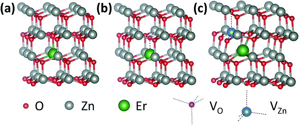 | ||
| Fig. 1 Relaxed structure model for three type of Er-doped ZnO defects. (a) ErZn, (b) ErZn–VO, (c) ErZn–VZn. The red, gray, and green balls are O, Zn, and Er atoms, respectively. The dash line linked pink or blue ball schematic indicates a O or Zn vacancy atom. | ||
3. Results and discussion
3.1 Crystal structure
To test the applicability and accuracy of the first-principles calculations method used in this study, we first calculated the lattice constants and electronic structure of bulk ZnO. As the band gap error, LDA/GGA underestimated the band gap of the semiconductor considerably. Our GGA calculated band gap of ZnO is 0.67 eV, which is much smaller than the experimental band gap of 3.37 eV.1 Therefore, following previous studies on ZnO,19,20 in this study, the GGA + U method is used to study the electronic and optical properties of Er-doped ZnO. Through our test, using Ud,Zn = 10.5 eV and Up,O = 7.0 eV, we obtained a direct band gap of 3.26 eV and lattice constants of a = 3.32 Å and c = 5.34 Å for bulk ZnO, which is close to the experiment results.1 This is meaningful to obtain proper results of the electronic and optical properties in ZnO.In Fig. 1, we show the relaxed three defect configurations ErZn, ErZn–VO, and ErZn–VZn in ZnO. We can see that there are some of atomic displacements for the ErZn, ErZn–VO. For ErZn defect, except the Er–O bond in the c direction is lengthened from 1.98 Å to 2.16 Å, which is caused by the large atom radius of Er. Other bond lengths have almost no change. In an ErZn–VO defect, as shown in Fig. 1(b), the remaining three Er–O bonds change from 2.03 Å to 2.05 Å showing slight lengthening. The distance between Er and the removed O atom is 2.00 Å, which is much less than 2.16 Å in an ErZn defect. The reason is, with O atom removed, the original ligand Zn–O bond should shorten because of a lack of Colum interactions by the removed O. At the same time, owing to the large atomic radius of Er, the Er–O bond tends to lengthen. With both these interactions, the Coulomb interaction by the removed O shortens the bond length, whereas the large atomic radius of Er increases the bond length; finally, the Er–O bond changes slightly from 2.03 Å to 2.05 Å. The distance between Er and the removal of an O atom change slightly. However, in the ErZn–VZn defect configurations, the structure shows great disorder after relaxation. As shown in Fig. 1(c), an Er atom moves prominently to the Zn vacancy direction and the displacement reaches 0.65 Å. The O atoms, which ligand with the Er atom and Zn vacancy in the c direction, have moved in the c direction 0.33 Å and 0.35 Å, respectively. These large displacements all show great disorder in ErZn–VZn defect configuration.
3.2 Electronic structure
The band structure and density of states relate closely to the optical properties of Er-doped ZnO. We calculated the electronic band structure and density of states after optimization of the geometry structure. Fig. 2 and 3 show the calculated spin polarized electronic band structure and PDOS of the three Er related defects. The valence band maximum was set to zero to compare easily with each other. From Fig. 2 and 3, we can see that Er-doped ZnO mainly shows bulk ZnO electronic properties; the Er atom has some effect on the electronic properties of ZnO. Next, we analyze them in detail. | ||
| Fig. 2 Calculated spin polarizes band structure for the three type of Er-doped ZnO defects. (a) ErZn, (b) ErZn–VO, (c) ErZn–VZn. The valence band maximum was set to zero. | ||
 | ||
| Fig. 3 Calculated partial density of states for the three types of Er-doped ZnO defects. (a) ErZn, (b) ErZn–VO, (c) ErZn–VZn. The valence band maximum was set to zero. | ||
Fig. 2(a) and (c) show a band gap ∼3.25 eV for ErZn and ErZn–VZn, which is similar to that of bulk ZnO. In addition, their conduction band minimum shows similar dispersion properties, which means that they may have similar optical properties to that of the bulk ZnO. The only differences are at values near 4.8 eV above the valence band maximum. In spin down, there is one degenerate defect state in the ErZn defect; see Fig. 2(a). However, in Fig. 2(c), the ErZn–VZn defect shows split defect states near 4.2 eV and 4.8 eV. This is caused by the structural distortion and different defect states. Compared to their PDOS in Fig. 3, we can identify that one of the defect states comes from O 2p electrons and the other one comes from Er 4f electrons.
In Fig. 2(b), at about 2.2 eV, there is one defect level in the forbidden band gap both in the spin up and spin down. Combined with PDOS in Fig. 3(b), we can identify that this defect level is caused by the Zn 4s and Er 4p electrons. This defect level comes from the dangling bonds of Zn and Er atoms, which is caused by the removal of an O atom.
Fig. 3 shows the calculated total and PDOS of individual O, Zn, and Er elements in ErZn, ErZn–VO, ErZn–VZn defects in ZnO. From Fig. 3 displaying the total PDOS of three defects, one can see that there are three zones for the total density of states, which mainly show the bulk ZnO properties. The −10 eV to −6 eV are contributed by the Zn 3d states. The −6 eV to 0 eV come from the O 2p electrons. Above the Fermi level, Zn 4s electrons contributed the major states. In −6.0 eV to 0 eV, there are also some Zn 3d states, which possess hybridization with O 2p and aid in the construction of the valence band edge of bulk ZnO. In Fig. 3, Er atoms show evident spin polarized properties in all three Er-related doping. In spin up, the Er 4f electrons are distributed in −10 eV to −6 eV. In spin down, they are distributed near −2 eV and 4.8 eV. These asymmetrically distributed electronic states caused a spin magnetic Er atom.
Fig. 3(b) presents the PDOS of ErZn–VO, which shows similar properties with ErZn in Fig. 3(a) except at about 2.0 eV, where it shows a small peak in both spin up and spin down. We can see that this small peak comes from the Zn 4s and Er 4p electrons. These states show nonmagnetic properties and are consistent with the Fig. 2(b) band structure of ErZn–VO.
In Fig. 3(c), except for the Er induced 4f state peak near 4.8 eV, there is an O 2p induced state peak at approximately 4.2 eV in spin down. This state peak is consistent with Fig. 2(c), which shows a defect level at about 4.2 eV in spin down. Clearly, this defect state will induce a net magnetic moment in ZnO, which will be shown in more detail below.
3.3 Magnetic properties
Our calculated Mulliken population analyses of the magnetic moment of ZnO with Er defects are listed in Table 1. In Table 1, the Mulliken population analyses magnetic moment for the Er atom and the entire system of three types of Er-doped ZnO are shown. Evidently, the Er atom induces about 3.0 μB magnetic moments in all three defect system. However, the magnetic moments of Er are caused by its 4f electrons, as discussed in the electronic structure of Fig. 2 and 3 above, which have no interaction with the band edge states, e.g., O 2p and Zn 3s or 3p electrons. The 4f electrons of Er will have no effects with host ZnO electronic structure as the select rule. Therefore, Er-related magnetic moment is only an atomic-like 3.0 μB magnetic moment and no magnetic moments are shown in the host ZnO.| ErZn | ErZn–VO | ErZn–VZn | |
|---|---|---|---|
| Er atom | 2.94 | 2.93 | 3.01 |
| System | 2.83 | 2.91 | 4.00 |
With only the ErZn–VZn defect, Table 1 shows a magnetic moment of about 1.0 μB except for Er 3.0 μB magnetic moment. This is consistent with Fig. 3(c) that O 2p shows a small peak in about 4.2 eV in spin down. To show this clearly, we draw out the isosurface of the magnetic moments for ErZn–VZn defect, as shown in Fig. 4. We can clearly see the magnetic moment isosurface around an Er atom and one around the O atom. The isosurface around the Er atom shows an atomic-like magnetic. The isosurface around of the Er atom shows an atomic-like magnetic property. Our isosurface results show that the 1.0 μB magnetic moment clearly comes from the unpaired 2p electrons at the ligand O atom. These magnetic results are consistent with the recent experiment by Chen H. M. and Liu X. C. et al.12,13 This Zn vacancy-induced ferromagnetism is also consistent with the observed ferromagnetism in pulsed laser deposition ZnO films.22,23
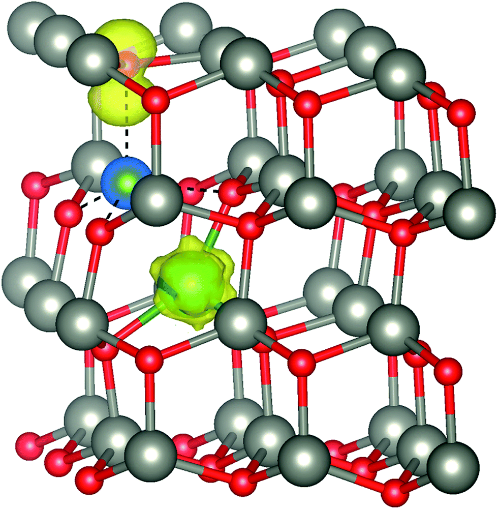 | ||
| Fig. 4 Spin density distribution (Δρ = ρup − ρdown) for ErZn–VZn defect in ZnO. The isosurface around the O atom shows the O 2p orbital properties. The isosurface level was 0.05 e Å−3. The dash line linked blue ball schematic shows a Zn vacancy. | ||
3.4 Optical properties
As an important optical material, the optical properties are important in the design of optical devices. Considering the anisotropy wurtzite structure of ZnO, we only give the optical properties in polycrystalline polarization for simplicity. The optical properties can be described by the complex dielectric function ε(ω) = ε1(ω) + iε2(ω). In the function, ε1(ω) and ε2(ω) are the real and imaginary part of the complex dielectric function, respectively. The other main optical spectra, such as the absorption coefficient I(ω), reflectivity R(ω), complex refractive index N(ω) = n(ω) + ik(ω), and energy-loss spectrum L(ω), can be obtained from the dynamic dielectric function.Fig. 5 shows the complex dielectric functions of ErZn, ErZn–VO, ErZn–VZn three defects in ZnO. For the optical device, the absorption coefficient is important. The absorption coefficient is shown in Fig. 6. We can see the absorption coefficient of three defects located mainly at 10 eV same as the bulk ZnO.
 | ||
| Fig. 5 Calculated real (a) and imaginary (b) part of the dielectric functions of ErZn, ErZn–VO, and ErZn–VZn three defects in ZnO. | ||
 | ||
| Fig. 6 Calculated absorption coefficients of ErZn, ErZn–VO, and ErZn–VZn three defects in ZnO. | ||
We first discuss the imaginary part, ε2, and then real part, ε1. The transitions obey the selection rule and electronic transitions between occupied and unoccupied states. For the defect of ErZn and ErZn–VZn, we can see in Fig. 5 that there are three main peaks of the imaginary part ε2, which are at around 5.2 eV, 9.0 eV and 15 eV. These results are consistent with the ZnO bulk optical properties and other theoretical results.20,24 For the ErZn–VO defect, there is a high peak at about 1.3 eV caused mainly by O vacancy defects.
For the real part ε1, we can see that the ErZn and ErZn–VZn still show similar results, however ErZn–VO defect shows a peak near 1.3 eV. Above 6.0 eV, three defects show a similar real part of the dielectric function. This similar profile means that the effects of Er and single intrinsic vacancy are mainly in lower energy optical properties and few on the high energy.
From Fig. 6, we can see that the absorption coefficients of all three defects of Er doping are located mainly at 10 eV, which falls in the vacuum ultraviolet region and show main bulk ZnO properties. Only the ErZn–VO defect shows a peak at about 1.3 eV, which is caused by O vacancy defects and is consistent with the previous complex dielectric function and band structure results.
From the optical properties results, we can see that although Er-doped ZnO induces some defect states, it still shows mainly ZnO optical properties. At a bandgap of about 3.26 eV, ZnO can be an excellent host material for Er ion doping and emission in the infrared region at 1.54 μm. Recently, Yang et al.6 realized red, green and blue multicolor electroluminescence using rare-earth Eu, Er, and Tm doped ZnO films acting as the lighting-emitting layer, respectively. In addition, Er doping can induce ferromagnetic properties in ZnO as shown above. This magnetic property for Er or other rare-earth-doped ZnO makes rare-earth-doped ZnO serve as a good candidate for spin optoelectronic studies.
4. Conclusion
In summary, first-principles calculations were performed to study the electronic structure, spin magnetic and optical properties of three defect configurations in Er-doped ZnO. The electronic and optical results show that Er-doped ZnO systems exhibit mainly ZnO bulk properties, which are essential for use in photoemission in the infrared application. The calculated electronic and magnetic results show that an Er atom always induces a magnetic moment of about 3.0 μB in the ZnO host. As the magnetic moment comes from the 4f electrons and there is no interaction with the band edge states of ZnO, the Er induce an atom-like magnetic moment shows atom-like magnetic and have no contribution to the ferromagnetism of Er-doped ZnO. Interestingly, these results show that the experimentally observed ferromagnetism of Er-doped ZnO comes from the O atom, which is the ligand with the Zn vacancy in Er-doped ZnO. Our calculated electronic and magnetic results prove this clearly. We think that this ferromagnetism mechanism of Er-doped ZnO can also be applied to other rare-earth-doped ZnO and is useful for spin optoelectronic applications in ZnO.Acknowledgements
This work was partly supported by the NSF of China (Grant No. 11104254) and Key Project of Science and Technology of Department of Education of Henan province (13A140225).References
- U. Ozgur, Y. I. Alivov and C. Liu, et al., J. Appl. Phys., 2005, 98, 041301 CrossRef.
- C. Liu, F. Yun and H. Morkoç, J. Mater. Sci.: Mater. Electron., 2005, 16, 555–597 CrossRef CAS.
- S. G. Kumara and K. S. R. K. Rao, RSC Adv., 2005, 5, 3306–3351 RSC.
- A. K. Pradhan, L. Douglas, H. Mustafa, R. Mundle, D. Hunter and C. E. Bonner, Appl. Phys. Lett., 2007, 90, 072108 CrossRef.
- P. T. Neuvonen, K. Sigvardt, S. R. Johannsen, J. Chevallier, B. Julsgaard, S. K. Ram and A. N. Larsen, Appl. Phys. Lett., 2014, 104, 102106 CrossRef.
- Y. Yang, Y. P. Li, C. X. Wang, C. Zhu, C. Y. Lv, X. Y. Ma and D. R. Yang, Adv. Opt. Mater., 2005, 2, 240–244 CrossRef.
- C. Ugolini, I. W. Feng, A. Sedhain, J. Y. Lin and H. X. Jiang, Appl. Phys. Lett., 2012, 101, 051114 CrossRef.
- Q. Wang, R. Hui, R. Dahal, J. Y. Lin and H. X. Jiang, Appl. Phys. Lett., 2010, 97, 241105 CrossRef.
- M. J. Soares, J. P. Leitão and M. I. N. da Silva, et al., Opt. Mater., 2011, 33, 1055 CrossRef CAS.
- S. J. Wang, X. Q. Wang, J. M. Li, Y. Jia and F. Wang, Mod. Phys. Lett. B, 2015, 21, 1550114 CrossRef.
- J. Qi, Y. H. Yang, L. Zhang, J. H. Chi, D. Q. Gao and D. S. Xue, Scr. Mater., 2009, 60, 289–292 CrossRef CAS.
- H. M. Chen, X. C. Liu, S. Y. Zhuo, Z. Xiong, R. W. Zhou, F. Li and E. W. Shi, AIP Adv., 2014, 4, 047121 CrossRef.
- W. B. Chen, X. C. Liu, F. Li, H. M. Chen, R. W. Zhou and E. W. Shi, AIP Adv., 2015, 5, 067105 CrossRef.
- P. P. Murmu, J. Kennedy, B. J. Ruck and J. Leveneur, Nucl. Instrum. Methods Phys. Res., Sect. B, 2015, 359, 1–4 CrossRef CAS.
- C. M. Yin, M. Rancic and G. G. de Boo, et al., Nature, 2013, 497, 91–94 CrossRef CAS PubMed.
- M. D. Segall, J. D. L. Philip and M. J. Probert, et al., J. Phys.: Condens. Matter, 2002, 14, 2717–2744 CrossRef CAS.
- J. P. Perdew, K. Burke and M. Ernzerhof, Phys. Rev. Lett., 1996, 77, 3865–3868 CrossRef CAS PubMed.
- R. S. Mulliken, J. Chem. Phys., 1955, 23, 1841–1845 CrossRef CAS.
- R. M. Sheetz, I. Ponomareva, E. Richter and A. N. Andriotis, Phys. Rev. B: Condens. Matter Mater. Phys., 2009, 80, 195314 CrossRef.
- Q. B. Wang, C. Zhou, J. Wu and T. Lu, Opt. Commun., 2013, 297, 79–84 CrossRef CAS.
- H. L. Li, Y. B. Lv, J. Z. Li and K. Yu, J. Alloys Compd., 2014, 617, 102–107 CrossRef CAS.
- Q. Xu, H. Schmidt and S. Zhou, et al., Appl. Phys. Lett., 2008, 92, 082508 CrossRef.
- G. Z. Xing, Y. H. Lu and Y. F. Tian, et al., AIP Adv., 2011, 1, 022152 CrossRef.
- J. Sun, H. T. Wang, J. L. He and Y. J. Tian, Phys. Rev. B: Condens. Matter Mater. Phys., 2005, 71, 125132 CrossRef.
| This journal is © The Royal Society of Chemistry 2016 |