
Dual-band photodetector with a hybrid Au-nanoparticles/β-Ga2O3 structure
Y. H. Anab,
D. Y. Guoab,
Z. M. Lic,
Z. P. Wuab,
Y. S. Zhiab,
W. Cuiab,
X. L. Zhaoab,
P. G. Li*ab and
W. H. Tang*ab
aLaboratory of Optoelectronics Materials and Devices, School of Science, Beijing University of Posts and Telecommunications, Beijing 100876, China. E-mail: whtang@bupt.edu.cn; pgli@zstu.edu.cn
bState Key Laboratory of Information Photonics and Optical Communications, Beijing University of Posts and Telecommunications, Beijing 100876, China
cUndergraduate Student from School of Information and Telecommunication Engineering, Beijing University of Posts and Telecommunications, Beijing 100876, China
First published on 8th July 2016
Abstract
Hybrid Au-nanoparticles (NPs)/β-Ga2O3 thin films were fabricated by laser molecular beam epitaxy of high quality β-Ga2O3 thin films on c-plane sapphire substrates followed by spin coating and post annealing of Au NPs. Photodetectors (PDs) made of hybrid Au-NPs/β-Ga2O3 thin films and bare β-Ga2O3 thin films are comparatively studied. It is found that Au-NPs can obviously improve the performances of PDs. Lower dark current, higher photoresponse and faster switching time under 254 nm light illumination are obtained by introducing Au-NPs. The localized surface plasmonic resonance from Au-NPs could be attributed to the enhanced performance. Meanwhile, a photoelectric response to 532 nm light illumination is observed in an Au NPs/β-Ga2O3 based PD. It is suggested that our hybrid Au-NPs/β-Ga2O3 PD could serve as a dual-band detector in one device.
1. Introduction
In recent years, β-Ga2O3, with a wide direct band gap (∼4.9 eV) and high thermal stability, has been considered as an attractive and promising material for solar-blind deep UV detectors,1–3 gas sensor materials,4 magnetic semiconductors5 and power devices.6 Among these applications, UV detectors have a significantly huge market in civil and military areas. So far, a lot of encouraging advances on β-Ga2O3-based detectors have been reported in terms of their low dark current, high responsivity and high sensitivity in a variety of detector structures such as films,3,7,8 single crystals9 and nanostructures.10–13 In spite of these advantages, the performance of β-Ga2O3-based UV detectors is still lower than expected. Surface plasmons (SPs)13,14 can decrease dark current and improve photocurrent. Fortunately, SPs can form a dual-band (visible and UV) response with Ga2O3 films by introduction of Au-NPs due to the absorption wavelength of Au NPs being around 532 nm. The advantage of dual-band PDs is that a PD can integrate two PDs, which significantly reduces size and cost.SPs, excited by the interaction between light and electron plasma waves at the metal surface, have been widely used to improve the efficiency of photovoltaics,15 photocatalysis,16 PDs and solar cells.17–20 Because of the localized field amplification that occurs, in metal NPs on the surface of the semiconductor, excitation of surface plasmons can enhance scattering and optical absorption of incident photons within the semiconductor region near each NP. Among the metals, the SPs of Au-NPs has been actively used to enhance PDs performance owing to chemical stability,20–24 and which has been continued interest in the plasmonic properties and sensing capabilities over the past 30 years.25–27 However, the dual-band response of PD has been far less experimental work. Besides, Au NPs unpin Fermi level at the metal–semiconductor interface suppress photogenerated carriers are captured from Ga2O3 thin film.28–30 Hence, it is worthwhile to explore the effect of Au NPs on the performance of PD. In this study, Au NPs/β-Ga2O3 hybrid PD that can be operated at 254 nm and 532 nm is fabricated. Meanwhile, the physical, electrical, and optical properties of the Au NPs/β-Ga2O3 hybrid PD are discussed.
2. Experimental details
The bare β-Ga2O3 epilayer films were grown on (0001) sapphire substrates by laser molecular beam epitaxy (L-MBE). A high-purity (99.995%) Ga2O3 ceramic was used as the target of L-MBE. Before depositing, the chamber was pumped to a vacuum degree of around 1 × 10⁻⁶ Pa. The laser ablation was carried out at a laser fluence of 5 J cm−2 with a repetition rate of 1 Hz using a KrF excimer laser with a wavelength of 248 nm. The distance between target and substrate was 5 cm, and the substrate was rotated during deposition to improve the film uniformity. The sample was deposited upon 1 × 10⁻³ Pa of oxygen pressure for 10![[thin space (1/6-em)]](https://www.rsc.org/images/entities/char_2009.gif) 000 pulse at 750 °C. The thicknesses of the films were estimated by scanning electron microscope (SEM) to be ∼400 nm. After the growth, Au colloids with about 30 nm size were deposited by spin coating method onto the Ga2O3 thin film, which was rotated at 450 rpm for 6 s following 4000 rpm 1 min by SIYOUYEN KW-4A/5 spin coater. After depositing by spin coating, the film was subsequently inserted into a tube furnace and annealed in atmosphere at 300 °C for 10 min in a furnace to evaporate the solvent and remove organic residuals. The surface morphologies were characterized by a Hitachi S-4800 SEM. The crystal structures were measured by a Bruker D8 Advance X-ray diffractometer (XRD). To construct a metal–semiconductor–metal photodetector, radio frequency magnetron sputtering technique was used to deposit four pairs of Au/Ti interdigital electrode on the β-Ga2O3 thin films using a shadow mask. The current–voltage (I–V) and time-dependent photoresponse of the bare β-Ga2O3 PD and Au NPs/β-Ga2O3 PD were measured by Keithely 2450. A 6 W lamp was employed to provide the 254 nm and 365 nm UV for the photocurrent measurement.
000 pulse at 750 °C. The thicknesses of the films were estimated by scanning electron microscope (SEM) to be ∼400 nm. After the growth, Au colloids with about 30 nm size were deposited by spin coating method onto the Ga2O3 thin film, which was rotated at 450 rpm for 6 s following 4000 rpm 1 min by SIYOUYEN KW-4A/5 spin coater. After depositing by spin coating, the film was subsequently inserted into a tube furnace and annealed in atmosphere at 300 °C for 10 min in a furnace to evaporate the solvent and remove organic residuals. The surface morphologies were characterized by a Hitachi S-4800 SEM. The crystal structures were measured by a Bruker D8 Advance X-ray diffractometer (XRD). To construct a metal–semiconductor–metal photodetector, radio frequency magnetron sputtering technique was used to deposit four pairs of Au/Ti interdigital electrode on the β-Ga2O3 thin films using a shadow mask. The current–voltage (I–V) and time-dependent photoresponse of the bare β-Ga2O3 PD and Au NPs/β-Ga2O3 PD were measured by Keithely 2450. A 6 W lamp was employed to provide the 254 nm and 365 nm UV for the photocurrent measurement.
3. Results and discussion
Fig. 1(a–c) show the SEM images of the bare β-Ga2O3 thin film, 40% Au NPs/β-Ga2O3 thin film and 100% Au NPs/β-Ga2O3 thin film (40% Au NPs means Au colloids diluted to 40%, and 100% Au NPs means Au colloids without diluting). The bare β-Ga2O3 thin film shows a dense and smooth surface morphology. The size of the uniform dispersal Au NPs is 30–40 nm. And Au NPs increase on the β-Ga2O3 thin film with increasing Au colloids concentration. The crystal structure of the Ga2O3 thin films were investigated by XRD patterns. Fig. 1(d) shows the XRD patterns of the bare Ga2O3 thin film, 40% and 100% Au NPs/β-Ga2O3 thin films. The sharp peaks of the three samples correspond to (![[2 with combining macron]](https://www.rsc.org/images/entities/char_0032_0304.gif) 01), (
01), (![[4 with combining macron]](https://www.rsc.org/images/entities/char_0034_0304.gif) 02) and (
02) and (![[6 with combining macron]](https://www.rsc.org/images/entities/char_0036_0304.gif) 03), which can be indexed as β-Ga2O3 (JCPDS file 43-1012). Except the diffraction peak of the substrate, no other peaks are found, indicating a single (01) plane orientation growth. Moreover, the intensity of the β-Ga2O3 peaks is nearly the same, indicating that the Au NPs on the surface of β-Ga2O3 thin film have no effect on the crystal quality of the films. Fig. 1(e) shows the UV-vis absorbance spectra of bare β-Ga2O3 thin film, 40% and 100% Au NPs/β-Ga2O3 thin films on sapphire substrates. It is observed that a significant absorption of the bare β-Ga2O3 thin film only exhibit a significant absorption edge at wavelengths about 250 nm. After introducing Au-NPs, the samples consist of two peaks obtained around 250 nm and 560 nm. Due to the characteristic surface plasmons band of Au NPs the second peak is observed at λ = 560 nm. We can also observe that the absorption peaks intensity increases with the increasing of Au NPs.
03), which can be indexed as β-Ga2O3 (JCPDS file 43-1012). Except the diffraction peak of the substrate, no other peaks are found, indicating a single (01) plane orientation growth. Moreover, the intensity of the β-Ga2O3 peaks is nearly the same, indicating that the Au NPs on the surface of β-Ga2O3 thin film have no effect on the crystal quality of the films. Fig. 1(e) shows the UV-vis absorbance spectra of bare β-Ga2O3 thin film, 40% and 100% Au NPs/β-Ga2O3 thin films on sapphire substrates. It is observed that a significant absorption of the bare β-Ga2O3 thin film only exhibit a significant absorption edge at wavelengths about 250 nm. After introducing Au-NPs, the samples consist of two peaks obtained around 250 nm and 560 nm. Due to the characteristic surface plasmons band of Au NPs the second peak is observed at λ = 560 nm. We can also observe that the absorption peaks intensity increases with the increasing of Au NPs.
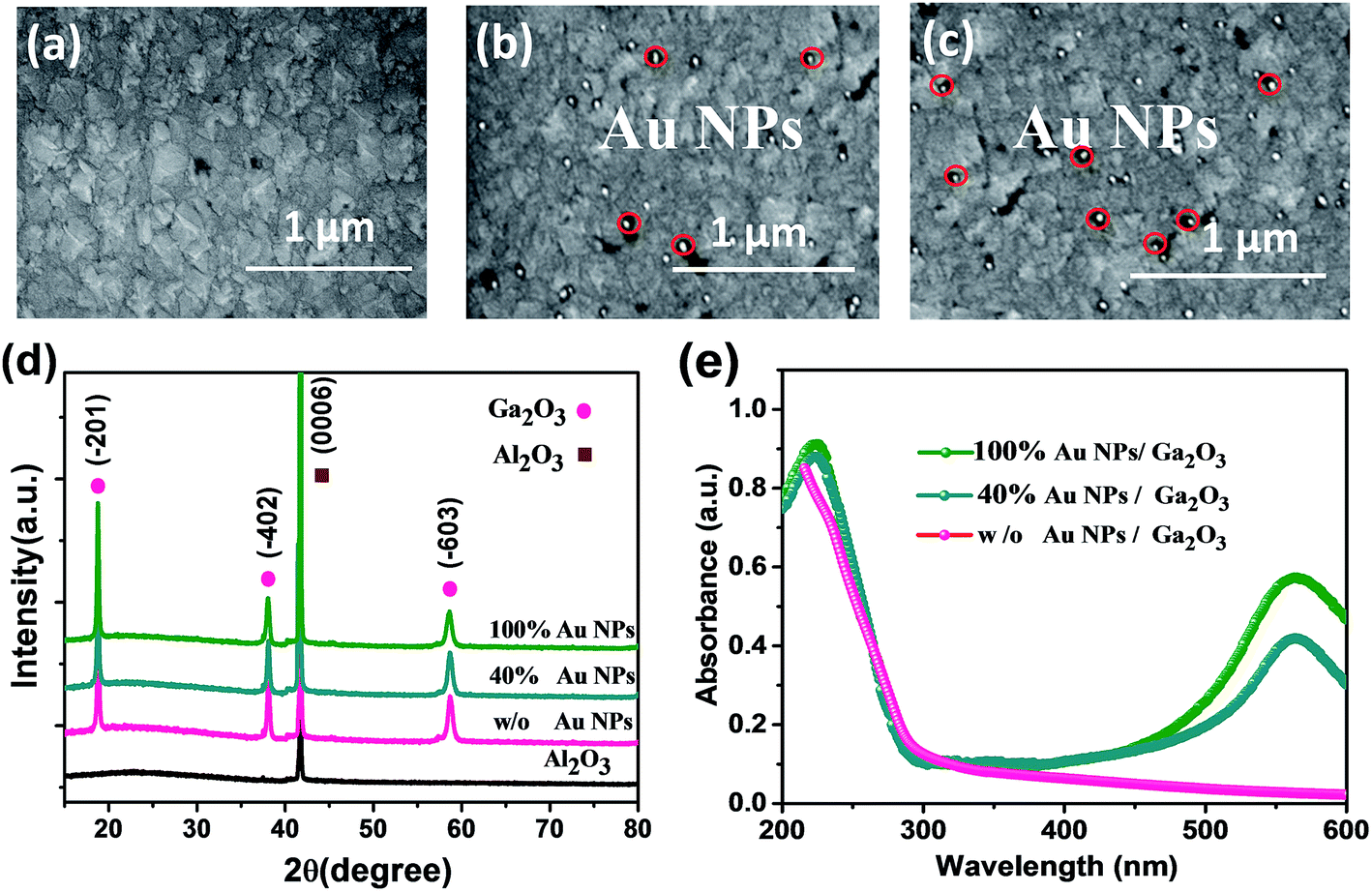 | ||
| Fig. 1 (a–c) are the SEM images of bare β-Ga2O3 thin film, 40% and 100% Au NPs/β-Ga2O3 thin film; (d) the XRD patterns of the pristine Ga2O3 film and other films with Au NPs for 30–40 nm; (e) UV/vis absorbance spectra of bare β-Ga2O3 thin film, 40% and 100% Au NPs/β-Ga2O3 thin film. | ||
The schematic diagram of the fabricated prototype PD device is shown in Fig. 2(a). The I–V characteristic curves of the bare β-Ga2O3, 40% and 100% Au NPs/β-Ga2O3 PDs under different illumination are shown in Fig. 2(b), (c) and (d), respectively. The linear I–V characteristics indicate that ohmic contact has been obtained. Among three PDs, the dark current of 100% Au NPs PD with 18.2 nA is smallest than that of 40% Au NPs/β-Ga2O3 PD (21.0 nA) and bare β-Ga2O3 PD (31.6 nA) at 1 V. And the photocurrent with 259.5 nA under 254 nm light illumination is largest than that of the 40% Au NPs/β-Ga2O3 PD (178.1 nA) PDs and bare β-Ga2O3 PD (126.0 nA) at 1 V. Meanwhile, we investigate the effect of 532 nm. It is obvious that the current of bare β-Ga2O3 PD increases as the applied bias increases both 254 nm and under 254 nm + 532 nm light illumination conditions, because absorption edge of β-Ga2O3 thin film is about 254 nm. The I–V curve with 37.2 nA measured under 532 nm illumination shows little increase, which may arise from the defects in β-Ga2O3 thin film. However, the I–V curves of 40% and 100% Au NPs/β-Ga2O3 PDs (73.2 nA and 49.3 nA) measured show obvious increase with increasing Au NPs under 532 nm light illumination, because absorption edge of Au NPs is located at around 532 nm. Furthermore, the I–V curves of 100% and 40% Au NPs/β-Ga2O3 PDs (317.5 nA and 212.9 nA) have significantly increased under 254 nm + 532 nm light illumination compared with 254 nm light illumination, due to the existence of SPs by Au NPs on the surface of β-Ga2O3 thin film.
 | ||
| Fig. 2 (a) The schematic illustration of the Au NPs/β-Ga2O3 PDs; (b), (c) and (d) are the I–V cures of bare β-Ga2O3 PD, 40% and 100% Au/β-Ga2O3 PDs upon different light illumination, respectively. | ||
To investigate the photo dual-band modulation, the time dependence of bare β-Ga2O3, 40% and 100% Au/β-Ga2O3 PDs in dark and under 254 nm, 532 nm and 254 + 532 nm light illumination (120 μW cm−2) at 1 V, as shown in Fig. 3(a–c). It can be clearly seen that the photocurrent of bare β-Ga2O3 PD responds sensitively only to 254 nm light illumination. Nevertheless, the photocurrents of 40% and 100% Au NPs/β-Ga2O3 PDs respond more and more sensitively to 254 nm and 532 nm light illumination with increasing Au NPs, respectively. In addition, they are enhanced under 254 nm + 532 nm light illumination. In order to further investigate the performance of these PDs, the transient response with a 1 V applied bias and at 254 nm light illumination measured as the UV excitation is switched on and off, as shown in Fig. 3(d). Three PDs exhibit excellent on–off switching performance. The currents of three PDs mostly exhibit two distinct states with the light irradiation on and off, a low-current state in dark and a high-current state under 254 nm light illumination. The current increases very sharply from one state to another state, indicating an obvious response speed of the two PDs. The results of the time-resolved photocurrent reveal that the response speeds of the PDs increase with increasing Au NPs. For further detailed comparison of the response time of three PDs, the quantitative analysis of the current rise and decay process involve the fitting of the photoresponse curve with a bi-exponential relaxation equation of the following type:31
 | (1) |
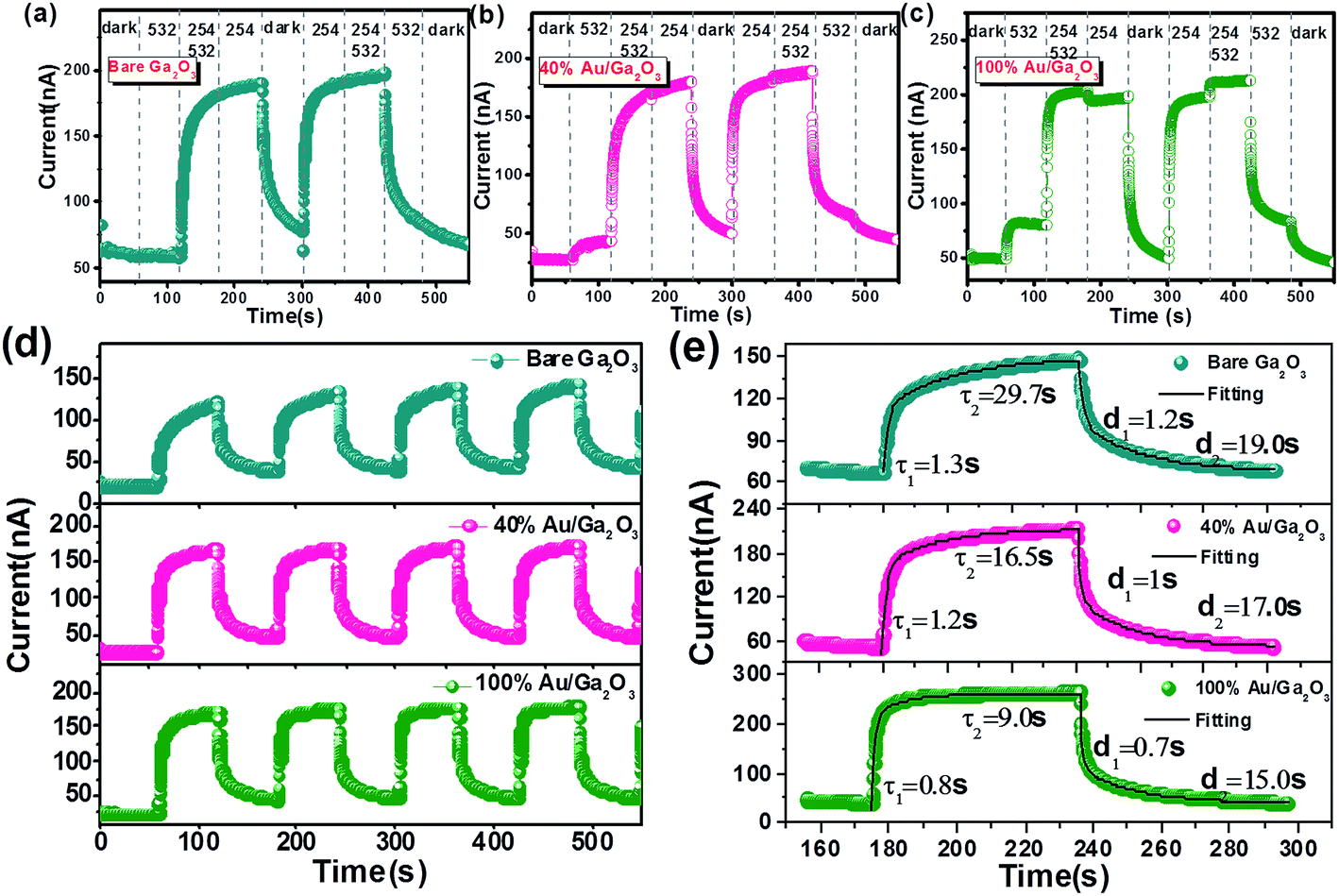 | ||
| Fig. 3 (a–c) are temporal responses of the three PDs measured by shutting on/off the 254 nm, 532 nm and 254 + 532 nm lights illumination (120 μW cm−2) under a 1 V applied bias. (d) and (e) are time-resolved photoresponse of the three PDs, respectively. The 254 nm light illumination (120 μW cm−2) were turned on/off manually to generate pulsed light. | ||
Fig. 4(a) show the values of dark current, photocurrent and photoconductive gain obtained for three PDs at 1 V. The dark current for a bare β-Ga2O3 based UV PD is about 31.6 nA (Table 1). The dark current for the 40% and 100% Au NPs/β-Ga2O3 PDs are about 21.0 and 18.2 nA. It is found that the value of dark currents of PDs obviously decreases with the increasing of Au NPs [Fig. 4(a)], due to the formation of a Schottky junction at the interface of the Au NPs with the semiconducting β-Ga2O3 thin film. Values of the rise time and fall time obtained for three PDs are plotted in Fig. 4(b). Both the rise time and fall time for PDs are reduced with increasing Au NPs.
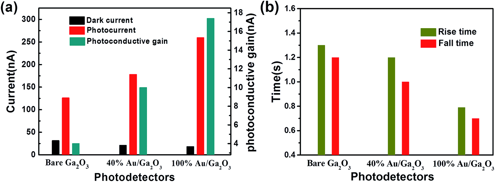 | ||
| Fig. 4 (a) Variations of dark current, photocurrent and photoresponse (K) of the fabricated UV PDs. (b) Variation of rise time and fall time of the fabricated UV PDs. | ||
| Samples prepared | Dark current (nA) | Photocurrent (nA) | Photoconductor gain Ion/Ioff | Rise time Tr (s) | Fall time Tf (s) |
|---|---|---|---|---|---|
| Bare Ga2O3 | 31.6 | 126.6 | 4.0 | 1.3 | 1.2 |
| 40% Au/Ga2O3 | 21.0 | 212.9 | 10.1 | 1.2 | 1.0 |
| 100% Au/Ga2O3 | 18.2 | 317.5 | 17.4 | 0.8 | 0.7 |
The photoconductive gains for PDs increase with increasing Au NPs (Table 1). The photoconductive gain (K) of a UV PD is determined as K = Ion/Ioff, where Ion is the photocurrent is measured under UV radiation and Ioff is the dark current measured in dark. The enhanced photoconductive gain obtained for the Au NPs/β-Ga2O3 PDs are attributed to two main factors. One is related to the obvious reduction in the value of low dark current due to formation of the Schottky barrier at the interface of β-Ga2O3 thin film and Au NPs. The other factor is SPs caused by Au NPs on the surface of β-Ga2O3 thin film, as discussed earlier.
Fig. 5(a–c) show the photocurrent response of the bare β-Ga2O3, 40% and 100% Au NPs/β-Ga2O3 PDs at the 1 V under 254 nm light illumination. The sequence of the test is with power densities range from 100 μW cm−2 → 50 μW cm−2 → 10 μW cm−2 → 50 μW cm−2 → 100 μW cm−2. The consequence demonstrates that the photocurrent increases steadily as the irradiance intensity increases, reaching 80 nA, 83 nA and 93 nA at 10 μW cm−2, respectively. And it can be seen that the photocurrent response detectors are extremely consistent and repeatable.
 | ||
| Fig. 5 (a–c) are the current versus time under various 254 nm light illumination intensities of the bare β-Ga2O3, 40% and 100% Au NPs/β-Ga2O3 PDs at 1 V. | ||
In order to illustrate the aforementioned mechanism, the energy band diagrams of β-Ga2O3 PDs without and with Au are plotted as shown in Fig. 6. Oxygen molecules are absorbed on the surface n-type β-Ga2O3 and decrease the carrier density in the β-Ga2O3 film by trapping free electrons [O2(g) + e− → O2−(ad)] from the n-type semiconductor.28 It created a depletion layer with low conductivity near the surface. When covered with Au NPs, which means a localized Schottky junction that will creates a charge depletion region, takes shape at the Au NPs–β-Ga2O3 interfaces. The negatively charged Au NPs deplete the carriers near the surface of β-Ga2O3 films. As the width of the depletion layer increases, the depletion region close to the Au NPs increase accordingly. And the width of the depletion layer is relevant to the barrier height. In addition, it is the reflection of the unpinned Fermi level at the metal–semiconductor interface.29,30 All of these cause the decreased dark current in Au NPs/β-Ga2O3 PD. And dark current decreased with increasing Au NPs on the β-Ga2O3 interfaces.
 | ||
| Fig. 6 Schematic illustrating the charge transfer process between β-Ga2O3 PDs without and with Au NPs. Upward band bending creates a Schottky barrier, which allows hot electrons with energy >Φb to inject into the conduction band of the Ga2O3 epilayer. | ||
When upon 254 nm light illumination, electron–hole pairs are generated [hν → e− + h+]. The photogenerated carriers immediately affect the photocurrent due to the sudden increase in the carrier density in the β-Ga2O3 film. Then, holes flow to the surface and recombine with the O2-trapped electrons and releasing O2− from the surface [O2−(ad) + h+ → O2(g)]. The remaining unpaired electrons become the major carriers that contribute to the photocurrent until they are trapped again. When covered with Au NPs, the SPs of the Au NPs have enhanced the scattering of the 254 nm light, which made more photons scatter on the β-Ga2O3 film. Then more photogenerated electron–hole pairs are created. The impact of SPs increases with the increasing of Au NPs. As a result, Au NPs/Ga2O3 PD exhibits significantly high value of photocurrent.
4. Conclusion
In this paper, we demonstrated that Au NPs on the surface of β-Ga2O3 thin film can improve the performance of PD. An obvious enhancement of the response sensitivity and good reproducibility for the Au NPs-decorated PD can be observed, and the performance of PD is enhanced with the increasing of the quantity of Au NPs. Meanwhile, dual-band (visible and UV) response is obtained with Ga2O3 PD by introducing Au-NPs and the absorption wavelength of Au NPs is around 532 nm. All these enhanced performances are attributed to the coupling between the excitons of β-Ga2O3 thin film and SPs of Au NPs. So, it is a viable approach to improve the performance of photodetectors.Conflict of interest
The authors declare no competing financial interest.Acknowledgements
This work was supported by Fund of State Key Laboratory of Information Photonics and Optical Communications (Beijing University of Posts and Telecommunications), People's Republic of China, the National Natural Science Foundation of China (Grant No. 51572033, 61274017, 51572241, and 11404029), the Fundamental Research Funds for the Central Universities (Grant No. 2014RC0906).References
- Y. H. An, D. Y. Guo, S. Y. Li, Z. P. Wu, Y. Q. Huang, P. G. Li, L. H. Li and W. H. Tang, J. Phys. D: Appl. Phys., 2016, 49, 285111 CrossRef.
- S. Nakagomi, T. Momo, S. Takahashi and Y. Kokubun, Appl. Phys. Lett., 2013, 103, 072105 CrossRef.
- D. Y. Guo, P. G. Li, Z. P. Wu, W. Cui, X. L. Zhao, M. Lei, L. H. Li and W. H. Tang, Sci. Rep., 2016, 6, 24190 CrossRef CAS PubMed.
- M. Fleischer, L. Höllbauer and H. Meixner, Sens. Actuators, B, 1994, 18, 119–124 CrossRef CAS.
- D. Y. Guo, Y. H. An, W. Cui, X. L. Zhao, Y. S. Zhi, M. Lei, L. H. Li, P. G. Li, Z. P. Wu and W. H. Tang, Sci. Rep., 2016, 6, 25166 CrossRef CAS PubMed.
- M. Higashiwaki, K. Sasaki, A. Kuramata, T. Masui and S. Yamakoshi, Appl. Phys. Lett., 2012, 100, 013504 CrossRef.
- T. Oshima, T. Okuno and S. Fujita, Jpn. J. Appl. Phys., 2007, 46, 7217 CrossRef CAS.
- D. Y. Guo, Z. P. Wu, P. G. Li, Y. H. An, H. Liu, X. C. Guo, H. Yan, G. F. Wang, C. L. Sun, L. H. Li and W. H. Tang, Opt. Mater. Express, 2014, 4, 1067–1076 CrossRef.
- T. I. Shin, H. J. Lee, W. Y. Song, S. W. Kim, M. H. Park, C. W. Yang and D. H. Yoon, Nanotechnology, 2007, 18, 345305 CrossRef.
- C. H. Liang, G. W. Meng, G. Z. Wang, Y. W. Wang, L. D. Zhang and S. Y. Zhang, Appl. Phys. Lett., 2001, 78, 3202–3204 CrossRef CAS.
- C. L. Kuo and M. H. Huang, Nanotechnology, 2008, 19, 155604 CrossRef PubMed.
- J. Y. Li, L. S. Wang, D. B. Buchholz and R. P. H. Chang, Nano Lett., 2009, 9, 1764–1769 CrossRef CAS PubMed.
- R. Liu, X. W. Fu, J. Meng, Y. Q. Bie, D. P. Yu and Z. M. Liao, Nanoscale, 2013, 5, 5294–5298 RSC.
- S. W. Hwang, D. H. Shin, C. O. Kim, S. H. Hong, M. C. Kim, J. Kim, K. Y. Lim, S. Kim, S. H. Choi, K. J. Ahn, G. Kim, S. H. Sim and B. H. Hong, Phys. Rev. Lett., 2010, 105, 127403 CrossRef PubMed.
- S. Mubeen, J. Lee, N. Singh, S. K. rämer, G. D. Stucky and M. Moskovits, Nat. Nanotechnol., 2013, 8, 247–251 CrossRef CAS PubMed.
- A. Marimuthu, J. Zhang and S. Linic, Science, 2013, 339, 1590–1593 CrossRef CAS PubMed.
- D. M. Schaadt, B. Feng and E. T. Yu, Appl. Phys. Lett., 2005, 86, 063106 CrossRef.
- Y. Jin, J. Wang, B. Sun, J. C. Blakesley and N. C. Greenham, Nano Lett., 2008, 8, 1649–1653 CrossRef CAS PubMed.
- M. L. Brongersma, N. J. Halas and P. Nordlander, Nat. Nanotechnol., 2015, 10, 25–34 CrossRef CAS PubMed.
- Z. Jin, L. Gao, Q. Zhou and J. Wang, Sci. Rep., 2014, 4, 4268 Search PubMed.
- C. Tian, D. Jiang, B. Li, J. Lin, Y. Zhao, W. Yuan, J. Zhao, Q. Liang, S. Gao, J. Hou and J. Qin, ACS Appl. Mater. Interfaces, 2014, 6, 2162–2166 CAS.
- J. F. Lu, C. X. Xu, J. Dai, J. T. Li, Y. Y. Wang, Y. Lin and P. L. Li, Nanoscale, 2015, 7, 3396–3403 RSC.
- A. Rajan, G. Kaur, A. Paliwal, H. K. Yadav, V. Gupta and M. Toma, J. Phys. D: Appl. Phys., 2014, 47, 425102 CrossRef.
- Z. Jin, L. Gao, Q. Zhou and J. Wang, Sci. Rep., 2014, 4, 4268 Search PubMed.
- L. A. Lyon, M. D. Musick and M. J. Natan, Anal. Chem., 1998, 70, 5177–5183 CrossRef CAS PubMed.
- V. I. Safarov, V. A. Kosobukin, C. Hermann, G. Lampel and J. Peretti, Phys. Rev. Lett., 1994, 73, 3584–3587 CrossRef CAS PubMed.
- G. C. Papavassiliou, J. Phys. F: Met. Phys., 1976, 6, L103 CrossRef CAS.
- Z. D. Huang, W. Y. Weng, S. J. Chang, Y. F. Hua, C. J. Chiu and T. Y. Tsai, IEEE Photonics Technol. Lett., 2013, 25, 1809–1811 CrossRef CAS.
- S. Lodha, D. B. Janes and N. P. Chen, J. Appl. Phys., 2003, 93, 2772–2779 CrossRef CAS.
- A. Chen, M. Young, W. Li, T. P. Ma and J. M. Woodall, Appl. Phys. Lett., 2006, 89, 233514 CrossRef.
- N. Liu, G. Fang, W. Zeng, H. Zhou, F. Cheng, Q. Zheng, L. Yuan, X. Zou and X. Zhao, ACS Appl. Mater. Interfaces, 2010, 2, 1973–1979 CAS.
| This journal is © The Royal Society of Chemistry 2016 |