
The characterization of graphene prepared using a nickel film catalyst pre-deposited to fused silica
Xianglian Songabc,
Lixin Songab,
Xiaoying Chenab and
Tao Zhang*ab
aThe Key Laboratory of Inorganic Coating Materials, Chinese Academy of Sciences, 1295 Dingxi Road, Shanghai 200050, PR China. E-mail: tzhang@mail.sic.ac.cn; Tel: +86-021-69906175
bShanghai Institute of Ceramics, Chinese Academy of Sciences, 1295 Dingxi Road, Shanghai 200050, PR China
cUniversity of Chinese Academy of Sciences, 19 Yuquan Road, Beijing 100049, PR China
First published on 9th February 2016
Abstract
Graphene was prepared using a nickel catalyst pre-deposited to a fused silica substrate through the chemical vapor deposition (CVD) process including a pre-annealing stage. The critical role of hydrogen in fabricating graphene successfully was confirmed by Raman spectra. Moreover, the purity of the graphene could be improved through adequate pre-annealing by suppressing the formation of graphite nano-rods. After the optimized CVD, it was observed that carbon atoms aggregated into tiny center spots and spread along the grain surfaces of the nickel layer, in contrast to the accumulation phenomenon on the grain boundaries. Furthermore, characterizations of the multilayer graphene (MLG) adhering directly on the fused silica were carried out, which would reflect the intrinsic properties of MLG grown on a nickel film.
1 Introduction
As a two-dimensional allotrope of carbon, graphene has attracted increasing attention since its first announcement in 2004.1 As a result of its excellent properties in thermodynamic stability, charge-carrier mobility, and transparency in the visible light range,2–5 graphene exhibits promise for application in many areas, such as transparent conductive electrodes, field effect transistors, super-conductors, etc. Compared with other common techniques to produce graphene, such as cleavage of graphite,6 decomposition of SiC,7 and reduction of graphene oxide (GO),8 chemical vapor deposition (CVD)9,10 has profound advantages in terms of high quality and large scale, and is regarded as one of the most promising methods for practical application.11,12In the precipitation of graphene through the CVD approach, nickel is a widely used catalyst due to its high carbon solubility and abundance.13–16 With nickel assistance, the synthesis of graphene involves at least two basic steps.17,18 Carbon atoms first undergo dissolution and diffuse into the nickel layer at high temperature, and secondly during the cooling process, segregate and crystallize to form graphene sheets. The segregation of carbon atoms for graphene formation on a nickel thin film can be moderated through appropriate annealing treatments during the CVD.19 It has been demonstrated that a particular pre-annealing stage before growth would provide multiple advantages in optimizing the nickel film,20,21 which is supposed to be an optimal parameter to improve the quality and purity of the formed graphene. However, research investigating the growth of graphene on nickel films through a CVD process with such a pre-annealing stage has rarely been reported.
In our work, the impacts of hydrogen and pre-annealing time on graphene growth were studied initially, so as to ensure the successful formation of a high purity graphene on the nickel thin film. After the optimized CVD, the segregation behavior of the carbon atoms on the whole surface of the nickel film were observed, whereas most research before focused mainly on the grain boundary area.22 Besides, when the samples were immersed into a FeCl3 solution, the graphene layers were obtained adhering directly to the surface of the fused quartz as the nickel layer was etched away, which reflected the true state of the graphene on the nickel surface. Furthermore, adhering graphene on transparent substrates is of great importance for electrical applications, especially for transparent conductive electrodes, which is regarded as a promising candidate to replace the widely used indium tin oxide (ITO).23 Currently, most graphene on transparent substrates is achieved with an extra transfer process, which would bring unexpected defects and reduced performance.24,25
2 Experimental
Nickel film with a thickness of ∼300 nm was deposited onto the fused silica using e-beam evaporation, which was loaded to the left side of a long quartz tube fixed in a sliding furnace CVD system (MTI, OTF-1200X-100SL). The furnace was firstly moved to the right side of the quartz tube to the pre-annealing temperature (Tpre-anneal). Then as the furnace was moved to the sample area at the left side of the quartz tube, the target samples were heated rapidly to Tpre-anneal in a steady flow of a hydrogen (H2, purity 99.99%) and argon (Ar, purity 99.99%) mixture. Later a stabilized pre-annealing stage was carried out at Tpre-anneal. Subsequently, a growth process was conducted at Tgrowth by introducing a flow of methane (CH4, purity 99.99%). After growth, the methane was shut off, and then the furnace was moved back to the right side. As a result, the samples were rapidly cooled down to room temperature. The entire CVD process was conducted under atmospheric pressure. Schematic diagrams of the CVD system and the CVD process are presented in Fig. 1. According to the gas and temperature schematic, the whole CVD process can be roughly divided into three stages in the experiment, as shown in Fig. 1(b). In stage I, the samples were heated up and kept at Tpre-anneal in the gas mixture of H2 and Ar. During stage II, CH4 was introduced as a carbon source for subsequent decomposition and growth. In stage III, these samples were cooled rapidly to room temperature by withdrawing the heating furnace.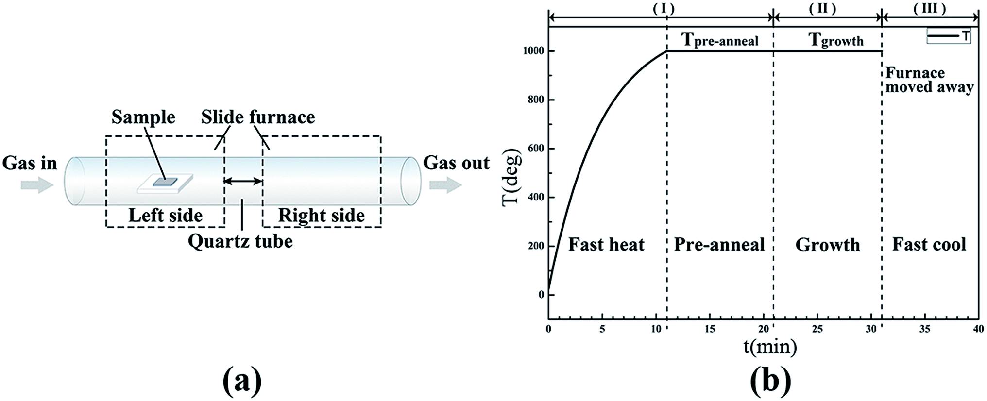 | ||
| Fig. 1 Schematic diagram of the CVD system (a) and the CVD process (b). | ||
The crystallographic properties of the samples were characterized using X-ray diffraction (XRD). Raman spectra were obtained using Renishaw equipment accompanied with a laser excitation at a wavelength of 514 nm. Chemical bond information was characterized using X-ray photoelectron spectroscopy (XPS) with a Kratos Axis Ultra spectrometer using a monochromatic Al Kα source. High-resolution scanning electron microscope (SEM) images were achieved using a Hitachi 8020 facility. The microstructures of the graphene sheets were examined using a high-resolution transmission electron microscope (HRTEM), the Tecnai G2 F20.
3 Results and discussion
3.1. The indispensable role of hydrogen in graphene synthesis
As shown in the XRD spectra in Fig. 2(a), a strong Ni(111) peak along with a weak Ni(200) can be observed in all the samples treated using the CVD processes with different H2 participation methods, which indicates the formation of dominant Ni(111) grains and a smaller population of Ni(200) grains in the nickel layer. The main Ni(111) orientation provides a perfect match for graphene growth, since the hexagonal lattice space of graphite (2.46 Å) is close to that of Ni(111) (2.497 Å).26 Moreover, a characteristic C(002) peak at 26.3° is observed, which is attributed to the carbon atoms dissolving in the nickel layer. The presence of hydrogen in stage II and stage III would be accompanied with a decline in the intensity of C(002), corresponding to a decrease in the concentration of carbon dissolved in the nickel layer as the precipitation occurs at the surface.27 | ||
| Fig. 2 (a) XRD and (b) Raman spectra of samples treated using various hydrogen conditions. | ||
On the other hand, typical Raman spectra were obtained for the samples to confirm the existence of graphene, as illustrated in Fig. 2(b). The graphene on the nickel surface displays characteristic peaks located at ∼1350 cm−1 (D band), ∼1580 cm−1 (G band) and ∼2700 cm−1 (2D band).11 The 2D peak, which originates from a double resonance process linking phonons to the electronic band structure,28 is normally adopted as powerful evidence to confirm the existence of graphene. With H2 participating in step I or in steps I/II, neither a typical G or 2D peak is detected. However, the distinctive Raman spectrum of graphene is obtained with H2 participating in all the three stages. The intensity ratios of D-peak to G-peak (ID/G) and 2D-peak to G-peak (I2D/G) are 0.49 and 1.22, respectively, which validates the existence of graphene.18 It should be noted that hydrogen is essential in the whole CVD process, especially in the cooling stage to successfully obtain graphene.
The effect of hydrogen at each stage can be summarized as follows. In stage I, hydrogen would eliminate contaminants and flatten the surface, which would provide a more uniform catalyst surface for further graphene formation.20,21 In stage II, hydrogen would promote methane absorption and decomposition, as well as carbon dissolution in the nickel layer.27,29 Most importantly, hydrogen in the cooling process would assist in carbon segregation on the nickel surface and assure the precipitation of high quality graphene.
3.2. The suppression of graphite nano-rod impurities
The extra pre-annealing treatment plays an important role in the CVD process to grow graphene of high purity. We investigated the influence of the pre-annealing time while the temperatures for pre-annealing and growth were maintained at 1000 °C. However, a nano-rod morphology, namely graphite nano-rods would appear on the nickel surface if the pre-annealing stage was inadequate. As shown in Fig. 3(a), two categories of Raman spectra corresponding to multilayer graphene (red color) and graphite nano-rods (blue color), were acquired simultaneously on samples pre-annealed for 6 min and grown for 10 min at 1000 °C. For the graphite nano-rods, merging peaks located at 1357 cm−1 and 1600 cm−1 were detected, which are attributed to the D and G peaks.30,31 | ||
| Fig. 3 (a) Raman spectra of the MLG and graphite nano-rods grown on a nickel film surface; SEM images of samples (b) pre-annealed for 6 min and grown for 10 min, (c) pre-annealed for 6 min and grown for 6 min, (d) pre-annealed for 10 min and grown for 10 min. | ||
As the SEM image in Fig. 3(b) shows, the nickel film pre-annealed for 6 minutes and grown for 10 minutes at 1000 °C is covered with graphite nano-rod clusters. Long rods gathering around the grain boundaries and particles of different sizes on the grain surface are found on the nickel film. The growth of the graphite nano-rods can be further observed by decreasing the growth time to 6 minutes, as shown in Fig. 3(c). This resulted in anomalous granules distributed along the grain-boundaries, and numerous much smaller tiny spots spread over the grain surfaces at the early stage. However, none of the graphite nano-rods can be found on the nickel surface any more as the pre-annealing time increases to 10 minutes, as shown in Fig. 3(d). Additionally, energy dispersive spectrometer (EDS) analyses were carried out to verify the nature of the nano-rod cluster, indicating that the cluster (A) has a higher percentage of carbon, and a corresponding lower percentage of nickel than the other area (B), as shown in Fig. 4. It is concluded that the increase in the pre-annealing time effectively prevents the unpredicted growth of graphite nano-rods on the nickel film surface.
 | ||
| Fig. 4 The EDS results evaluated from the areas (A) with and (B) without graphite nano-rods on a nickel film pre-annealed for 6 min and grown for 10 min. | ||
3.3. The segregation of carbon atoms on the nickel film surfaces
After the optimized CVD process, the segregation of carbon atoms on the nickel film surface is clearly obvious, which would clarify the precipitation phenomenon. As shown in Fig. 5, graphene is obtained on the surface of the nickel film, and the darker contrasts are responsible for multilayer graphene layers.32 It can be observed in Fig. 5(a) that carbon atoms accumulate along the grain-boundaries, relating closely to the high curvature and thus high density of atomic steps at the boundaries.20,21 Furthermore, for the grain surfaces of the nickel film, darker contrasts can be found around the tiny spots (Fig. 5(b)). The segregation of carbon on the grain surfaces of the nickel film is thought to start from tiny center spots and proceed outward, with spreading steps observed in Fig. 5(c). These spots on the grain surfaces could “pump” carbon atoms out of nickel layer, spread them along the surface, and form multilayer graphene near the center and formulate a single/bilayer at a distance. As a result, multiple-layers and single/bilayer graphene are recognized on the nickel film. In addition, visible wrinkles could be observed connecting with active spots in Fig. 5(b), which are related to the stress release arising from the deviation of thermal expansion coefficients between the nickel and graphene.16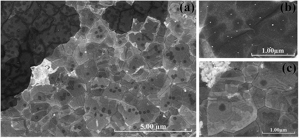 | ||
| Fig. 5 (a) Morphological characterization of carbon atom segregation on a nickel film surface, (b) and (c) high resolution SEM images of the grain boundary areas and grain surfaces of the nickel catalyst after the CVD process. | ||
3.4. Graphene attaching directly to fused silica after etching
The segregation of carbon atoms to form MLG on the surface of the nickel thin film is obvious, and the multilayer graphene would adhere directly onto the substrate surface when immersed in a ferric chloride (FeCl3) solution with a concentration of 0.1 mol L−1, as confirmed by the Raman spectrum (Fig. 6(a)). From the position and shape of the Raman peaks, it could be determined that multilayer and monolayer/bilayer graphene existed at the same time on surface of the fused quartz. The 2D peak of the multilayer graphene is much lower than the G peak, with a minor shift to a higher energy.28 In addition, the 2D peak of the monolayer/bilayer graphene has a single Lorentzian profile, and the intensity ratio of the 2D-peak and G-peak is higher than 1.20 Because of the phonon scattering in the lattice defects,12 a small band at the position of ∼1608 cm−1 can be also recognized. An extra analysis of the chemical state was carried out using XPS on the film surface, as shown in Fig. 6(b). A dominant peak located at ∼284.8 eV originating from the C–C sp2 bonding33 is recognized, verifying the existence of graphene on the surface of fused silica. | ||
| Fig. 6 (a) Raman spectra and (b) XPS results of the C1s peak of the MLG on the fused silica after FeCl3 etching. Cross-sectional TEM images of the MLG on (c) the nickel film (before etching) and on (d) the fused silica (after etching). | ||
TEM specimens of the MLG grown on the nickel surface and the MLG adhering to the fused silica were fabricated using focus ion beam (FIB) technology for cross-sectional observation. As shown in Fig. 6(c), before etching, multilayer graphene has been grown on the nickel film surface, whereas no graphene sheets can be observed at the interface between the nickel and fused quartz. The results indicate that the segregation of carbon atoms is easier on the top surface of the nickel layers than at the interface. However, multilayer graphene was apparent on the fused silica surface after the etching treatment with a FeCl3 solution, as shown in the TEM image in Fig. 6(d). The distance between layers is measured to be 0.349 nm, as shown in the inset image displayed in Fig. 6(d). Moreover, discontinuous points exist in the multilayer graphene on the fused quartz at the same time, which coincides with the D-band detected in the Raman spectrum.
In Fig. 7, the transparency (400 nm to 1500 nm) of the multilayer graphene adhering directly to the fused silica is compared with blank fused silica, and with multilayer graphene obtained through a conventional transferring process16 with PMMA assistance. It can be observed that the transparency of the MLG adhering directly to the quartz is higher than that obtained using a conventional transferring process, for which the transmittance is ∼90% at the 700–1500 nm wavelength. Moreover, the sheet resistance of the MLG (0.9–1.2 kΩ sq−1) adhering directly to the fused silica is much lower than the transferred film (2.2–2.6 kΩ sq−1), which is acquired using a four-probe measurement. In fact, the MLG samples acquired from the two methods both originate from the nickel film surface, and are supposed to have similar properties. The properties of the MLG obtained from direct adherence have a better coincidence with those of the MLG obtained on the nickel surface, and would be better suited to the practical application of graphene.
 | ||
| Fig. 7 Optical transparence of MLG obtained by adhesion and transfer with blank fused silica. | ||
4 Conclusion
In summary, we have adopted an optimized thermal CVD process including an extra pre-annealing process to synthesis graphene using a nickel catalyst pre-deposited to fused silica. It was established that hydrogen plays an essential role in promoting the formation of graphene, especially in the cooling stage. Moreover, the purity of formulated graphene can also be improved with subsequent pre-annealing time. The optimized CVD contributes to the segregation of carbon atoms on the nickel film, which further illustrates the formation mechanism of graphene, and provides a new insight for the direct growth of graphene on transparent dielectric substrates.References
- K. S. Novoselov, A. K. Geim, S. V. Morozov, D. Jiang, Y. Zhang, S. V. Dubonos, I. V. Grigorieva and A. A. Firsov, Science, 2004, 306, 666–669 CrossRef CAS PubMed.
- J. C. Meyer, A. K. Geim, M. I. Katsnelson, K. S. Novoselov, T. J. Booth and S. Roth, Nature, 2007, 446, 60–63 CrossRef CAS PubMed.
- K. S. Novoselov and A. K. Geim, Nat. Mater., 2007, 6, 183–197 CrossRef PubMed.
- A. V. Tyurnina, K. Tsukagoshi, H. Hiura and A. N. Obraztsov, Carbon, 2013, 52, 49–55 CrossRef CAS.
- R. S. Edwards and K. S. Coleman, Nanoscale, 2012, 5, 1–13 Search PubMed.
- L. Zhang, X. Li, Y. Huang, Y. Ma, X. Wan and Y. Chen, Carbon, 2010, 48, 2367–2371 CrossRef CAS.
- P. Lauffer, K. V. Emtsev, R. Graupner, T. Seyller, L. Ley and S. A. Reshanov, Phys. Rev. B: Condens. Matter Mater. Phys., 2008, 77, 155426 CrossRef.
- H. Tanaka, S. Obata and K. Saiki, Carbon, 2013, 59, 472–478 CrossRef CAS.
- A. Reina, X. Jia, J. Ho, D. Nezich, H. Son and V. Bulovic, Nano Lett., 2009, 9, 30–35 CrossRef CAS PubMed.
- N. Campos, A. M. Perez-Mas, P. Alvarez, R. Menendez and D. Gomez, Appl. Surf. Sci., 2015, 349, 101–107 CrossRef CAS.
- S. Bae, H. Kim, Y. Lee, X. Xu, J. S. Park and Y. Zheng, Nat. Nanotechnol., 2010, 5, 574–578 CrossRef CAS PubMed.
- G. Nandamuri, S. Roumimov and R. Solanki, Nanotechnology, 2010, 21, 145604 CrossRef CAS PubMed.
- Z. Fogarassy, M. H. Rummeli, S. Gorantla, A. Bachmatiuk, G. Dobrik, K. Kamaras, L. P. Biro, K. Havancsak and J. L. Labar, Appl. Surf. Sci., 2015, 314, 490–499 CrossRef.
- R. S. Edwards and K. S. Coleman, Acc. Chem. Res., 2013, 46, 23–30 CrossRef CAS PubMed.
- C. Y. Chen, D. Dai, G. X. Chen, J. H. Yu, K. Nishimura, C. T. Lin, N. Jiang and Z. L. Zhan, Appl. Surf. Sci., 2015, 346, 41–45 CrossRef CAS.
- X. Li, W. Cai, L. Colombo and R. S. Ruoff, Nano Lett., 2009, 9, 4268–4272 CrossRef CAS PubMed.
- A. Dahal and M. Batzill, Nanoscale, 2014, 6, 2548–2562 RSC.
- Q. Yu, J. Lian, S. Siriponglert, H. Li, Y. P. Chen and S. S. Pei, Appl. Phys. Lett., 2008, 93, 113103 CrossRef.
- Q. Yu, J. Lian, S. Siriponglert, H. Li, Y. Chen and S. Pei, Appl. Phys. Lett., 2008, 93, 113103 CrossRef.
- Y. Zhang, T. Gao, S. Xie, B. Dai, L. Fu and Y. Gao, Nano Res., 2012, 5, 402–411 CrossRef CAS.
- Y. Zhang, L. Gomez, F. N. Ishikawa, A. Madaria, K. Ryu, C. Wang and J. Phys, Chem. Lett., 2010, 1, 3101–3107 CAS.
- C. Lu, C. Jin, Y. Lin, C. Huang, K. Suenage and P. Chiu, Langmuir, 2011, 27, 13748–13753 CrossRef CAS PubMed.
- Y. Yi, L. Song, X. Song and T. Zhang, J. Alloys Compd., 2013, 281, 133–138 Search PubMed.
- L. G. De Arco, Y. Zhang, C. W. Schlenker, K. Ryu, M. E. Thompson and C. Zhou, ACS Nano, 2010, 4, 2865–2873 CrossRef PubMed.
- Y. Lee, S. Bae, H. Jang, S. Jand, S. E. Zhu, S. H. Sim, Y. I. Song, B. H. Hong and J. H. Ahn, Nano Lett., 2010, 10, 490–493 CrossRef CAS PubMed.
- S. Thiele, A. Reina, P. Healey, J. Kedzierski, P. Wyatt and P. L. Hsu, Nanotechnology, 2010, 21, 015601 CrossRef PubMed.
- M. Losurdo, M. M. Giangregorio, P. Capezzuto and G. Bruno, Phys. Chem. Chem. Phys., 2011, 13, 20836–20843 RSC.
- A. C. Ferrari, J. C. Meyer, V. Scardaci, C. Casiraghi, M. Lazzeri, S. Piscanec, D. Jiang, K. S. Novoselv, S. Roth and A. K. Geim, Phys. Rev. Lett., 2006, 97, 187401 CrossRef CAS PubMed.
- L. Baraton, Z. B. He, C. S. Lee, C. S. Cojocaru, M. Châtelet and J. L. Maurice, Europhys. Lett., 2011, 96, 46003 CrossRef.
- W. Yen, Y. Chen, C. Yeh, J. He, P. Chiu and Y. Chueh, Sci. Rep., 2014, 4, 4739 Search PubMed; R. Zhang, Z. S. Wang, Z. D. Zhang, Z. G. Dai, L. L. Wang and H. Li, Appl. Phys. Lett., 2013, 102, 193102 CrossRef CAS.
- T. Takami, R. Seino, K. Yamazaki and T. Ogino, J. Phys. D: Appl. Phys., 2014, 47, 094015 CrossRef.
- Y. Lee and J. H. Ahn, J. Appl. Phys., 2013, 113, 194305 CrossRef.
- A. N. Obraztsov, E. A. Obraztsova, A. V. Tyurnina and A. A. Zolotukhin, Carbon, 2007, 45, 2017–2021 CrossRef CAS.
| This journal is © The Royal Society of Chemistry 2016 |