Fabrication of Cu1.8S/CuS nanoplates counter electrode via alternating current etching for quantum dots-sensitized solar cells
Linlin Quan,
Weiping Li*,
Liqun Zhu,
Xiaowen Chang and
Huicong Liu*
Key Laboratory of Aerospace Materials and Performance (Ministry of Education), School of Materials Science and Engineering, Beihang University, Beijing 100191, China. E-mail: liweiping@buaa.edu.cn; liuhc@buaa.edu.cn; Fax: +86 1082317113; Tel: +86 1082317113
First published on 23rd June 2014
Abstract
We demonstrate a method for fabricating a Cu1.8S/CuS nanoplate counter electrode (CE) via the alternating current (AC) etching of brass. The photoelectrochemical performance and electrocatalytic properties of Cu1.8S/CuS CE with a η value of 3.22% are much higher than those of Pt and conventional Cu2S CEs. Furthermore, it offers a simple and low cost method for producing CuS counter electrodes in the future.
1. Introduction
In the past few years, quantum dot-sensitized solar cells (QDSCs) have attracted considerable attention. QDSCs have emerged as a promising candidate for the development of next generation solar cells because of their acceptable power conversion efficiency, ease of fabrication, and low production cost.1,2 QDSCs are based on the photosensitization of wide band gap semiconductor photoanodes (TiO2, ZnO, SnO2, etc.) with quantum dots (QDs) (such as CdS,3 CdSe,4 and PbS (ref. 5 and 6)), which make it possible to tune the absorption threshold by choosing the dot diameter, provide high luminescence quantum efficiency and more stability than dyes.7,8The counter electrode (CE) is a critical component in QDSCs, where electrons are injected into a polysulfide electrolyte. In DSSCs, Pt is usually used as the CE owing to its stability and high catalytic activity for the reduction of I3−.9,10 However, Pt is not very catalytic in a polysulfide electrolyte. This is because the sulfur present in the polysulfide electrolyte chemisorb on platinum surfaces and induce poisoning effects toward the electrode performance, which results in low fill factors and conversion efficiency.11–14
In order to increase the efficiency of QDSCs, metal sulfides, such as cobalt sulfide (CoS),24 iron sulfide,19 lead sulfide (PbS),15,16 nickel sulfide (NiS),12 Cu2ZnSnS4,14 and copper sulfide (Cu2S and CuS),12,17 have been employed as efficient CEs in the fabrication of QDSCs containing polysulfide electrolyte as a redox couple. Among them, Cu2S and CuS have been most commonly and efficiently used as CEs for QDSCs in recent years. Most recently reported Cu2S CEs are made by exposing the Cu metal to a sulfide solution. The black Cu2S film is easy to peel off from the Cu substrate,12,18,19 but the tendency of a continual reaction with a polysulfide electrolyte on a Cu substrate is the serious drawback of this method, which may make Cu2S CE unstable. Other methods of fabricating Cu2S or CuS include chemical bath deposition and hydrothermal methods. The advantage of using these methods could be used to prepare pure Cu2S or CuS with fewer crystal defects, but these methods need high-level equipment, high experimental conditions and complex processes. Furthermore, these methods using FTO as a carrier may decrease the interfacial binding force between FTO and the film. The adhesion intensity of the electrocatalytic active materials on the FTO substrate used as the counter electrode is a very important factor for determining the η of QDSCs.20 If the materials cannot stick to the FTO substrate, they may be released into the electrolyte, which depresses the stability of CE and solar cells.17
In the present study, we developed a new method via AC etching of brass to obtain a Cu1.8S/CuS nanoplate CE on a Cu micro-nanostructure. A Cu1.8S/CuS film by an in situ reaction was synthesized based on the Cu micro-nanostructure that could allows an effective control of the surface morphology and film thickness through AC etching. It is obvious that the large specific surface areas of Cu1.8S/CuS nanoplates improve the electrocatalytic activity for the polysulfide electrolyte. The interfacial binding force and conductivity of the Cu1.8S/CuS film on the brass substrate are obviously superior to a Cu2S film on FTO. At the same time, AC etching is simple to operate, uses less equipment and is low-cost. In addition, the photoelectrochemical performance of Cu1.8S/CuS CE is much higher than Pt and Cu2S.
2. Experimental section
2.1. Preparation
Sulphur sublimed (A.R.), sodium sulfide (A.R. Na2S·9H2O) and polyethylene glycol (M.W. 20![[thin space (1/6-em)]](https://www.rsc.org/images/entities/char_2009.gif) 000) were purchased from Beijing Yili Fine Chemicals Co., Ltd (China). Selenium powders (A.R.) and ethanol were supplied by Beijing Chemical Works (China). Cadmium nitrate (A.R. Cd(NO3)2·4H2O), sodium sulfite (A.R. Na2SO3) and zinc nitrate (A.R. Zn(NO3)2·6H2O) were purchased from Tianjin Jinke Fine Chemicals Co., Ltd (China).
000) were purchased from Beijing Yili Fine Chemicals Co., Ltd (China). Selenium powders (A.R.) and ethanol were supplied by Beijing Chemical Works (China). Cadmium nitrate (A.R. Cd(NO3)2·4H2O), sodium sulfite (A.R. Na2SO3) and zinc nitrate (A.R. Zn(NO3)2·6H2O) were purchased from Tianjin Jinke Fine Chemicals Co., Ltd (China).
2.2. Characterization
The surface morphology and composition of the samples were evaluated by scanning electron microscopy (SEM, JSM-6010LA) equipped with an EDS system and transmission electron microscopy (TEM, F20) equipped with an energy dispersive X-ray (EDX) spectroscope system. Atomic force microscopy (AFM, Veeco DI, USA) was used to measure the surface roughness. The X-ray diffraction (XRD) patterns of the samples were recorded on a Rigaku D/MAX-RB diffractometer with monochromatized Cu Kα radiation (k = 1.5418) at a scan rate of 6° min−1. The digital photographs were obtained using a digital camera (Olympus E-PL1, Japan).The photocurrent–voltage (J–V) of the QDSCs was recorded under illumination with a xenon lamp (500 W). The illumination intensity was 100 mW cm−2 and the range of wavelengths was 380–700 nm. A two-electrode photoelectrochemical cell was constructed and the electrolyte was an aqueous solution containing 2 M Na2S and 3 M S.19 A CHI 600A electrochemical analyzer was applied to record the J–V curves under illumination with an active area of 1 cm2.
Electrochemical impedance spectra (EIS) and Tafel polarization measurements with a scan rate of 10 mV s−1 were conducted in a symmetrical dummy cell fabricated with two identical CEs using a CHI 600A electrochemical analyzer in dark. The measured frequency for EIS ranged from 10 mHz to 1 MHz and the amplitude was set to 10 mV. The spectra were fitted by ZSimpWin software.
3. Results and discussion
Fig. 1 illustrates the preparation of Cu1.8S/CuS CE. First, we obtain the Cu micro-nanostructure through AC etching of brass. In this progress, zinc strips from the surface of the brass and can form a porous structure, which clearly increases the specific surface area. The etched brass is then dipped in polysulfide electrolyte for 5 min and we obtain the CE with nanoplates. | ||
| Fig. 1 Scheme of the preparation of Cu1.8S/CuS CE. | ||
SEM was used to evaluate the surface morphology of the samples at different preparation stages. Fig. 2(A–C) shows the digital photographs of the bare, etched and sulfurized brass, respectively. It can be readily indicated that bare brass becomes red after AC etching and becomes black after immersion in a polysulfide electrolyte. Furthermore, the black film on the brass is stable after a long period of time.
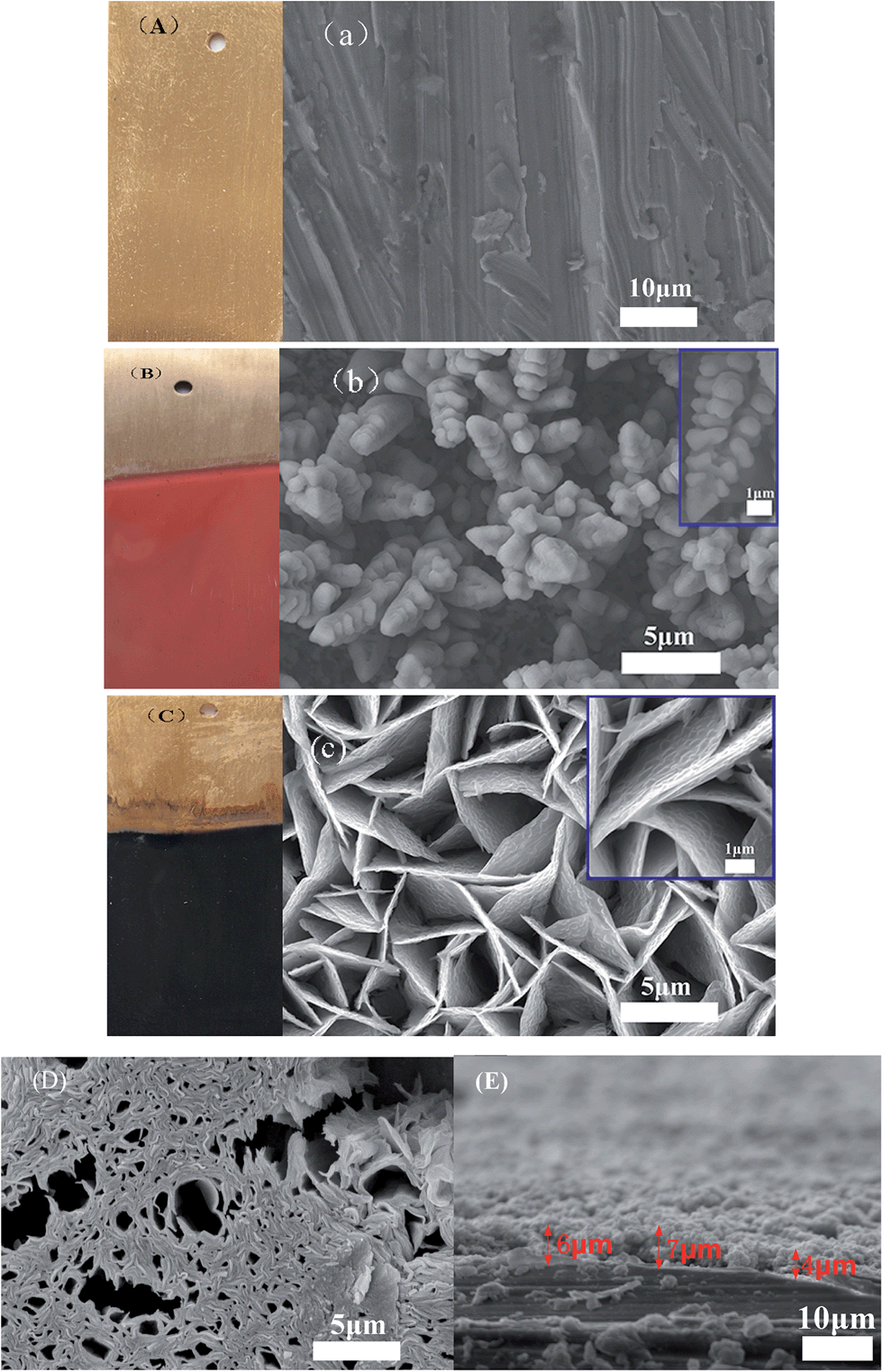 | ||
| Fig. 2 Digital photographs of (A) bare (B) etched and (C) sulfurized; SEM images of the surfaces (a) bare, (b) etched and (c) sulfurized brass; (D) SEM images of Cu2S on pure Cu substrate and (E) cross-sectional SEM images of Cu1.8S/CuS electrode. | ||
Before etching, brass has a coarse morphology with many obvious scratches due to mechanical polishing [Fig. 2(a)]. After etching for a period of time, the etched brass presents a hierarchical microstructure with a pinecone-like morphology [Fig. 2(b)]. When the etched brass plates are immersed in the polysulfide electrolyte, nanoplates can be observed on the sulfurized brass [Fig. 2(c)]. At higher magnification, we can clearly see nanoplates with a scaly structure. In Fig. 2(D), the film layer structures are not evenly distributed and there are many large pores. Fig. 2(E) indicates that the thickness of the black film is about 4–7 μm.
To study the growth process from a pinecone-like morphology to a nanoplate morphology, different morphologies were obtained after different growth times, as shown in Fig. 3. After immersing for 1 s, the original pinecone-like morphology changed and some needle-like whiskers emerged. By extending the immersion duration to 30 s, the buds bloomed like flowers and the nanoplate structure appeared. As immersion was further extended to 5 min, as shown in Fig. 3(d), a typical nanoplate morphology was formed. The nanoplate structure changed slightly after the immersion duration was extended to 1 h.
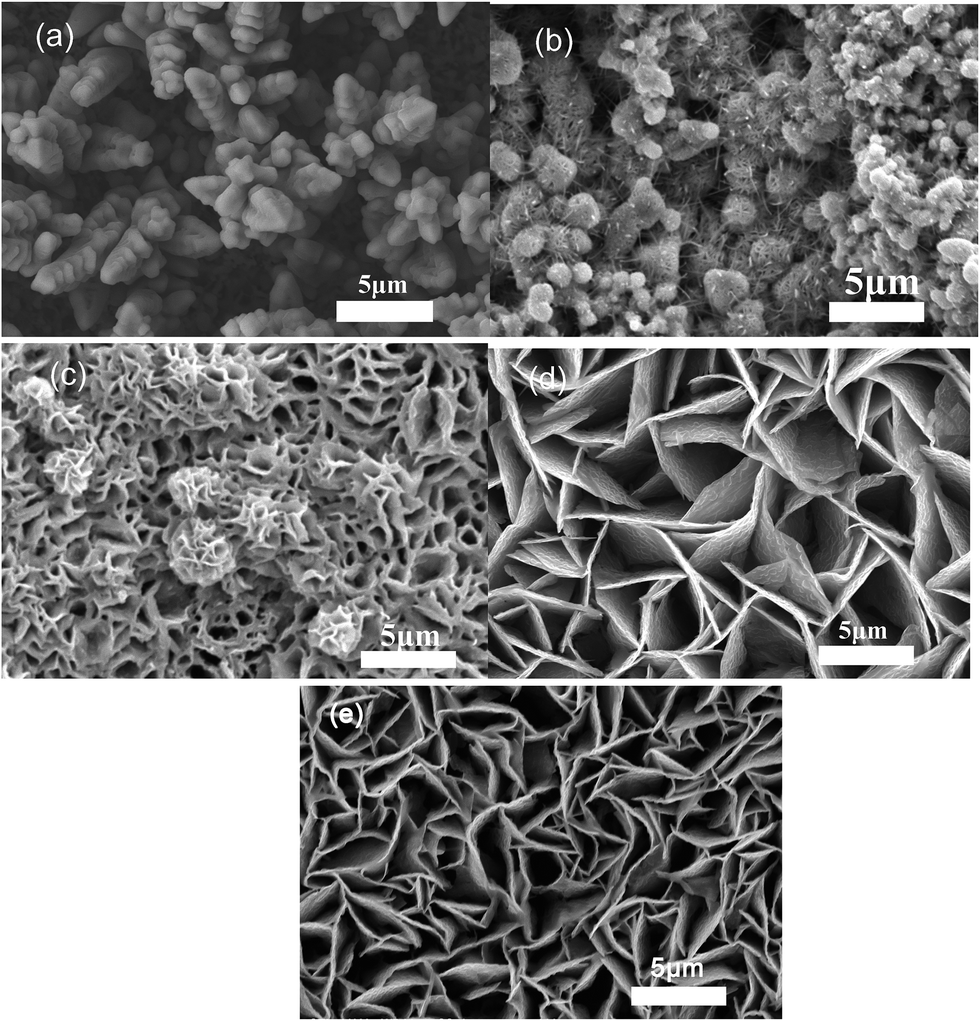 | ||
| Fig. 3 SEM images of etched brass plates immersed into a polysulfide electrolyte for different times (a) 0 s, (b) 1 s, (c) 30 s, (d) 5 min, (e) 1 h. | ||
Fig. 4 shows XRD patterns of the samples at different preparing stages. The peaks at 42.3°, 49.3°, 72.2° and 87.5° 2θ correspond to the diffraction peaks of Cu0.64Zn0.36 (JCPDS no. 50-1333), respectively. After AC etching, new peaks corresponding to the diffraction peaks of Cu (JCPDS no. 04-0836) appeared at 43.3°, 50.4° and 74.1° 2θ, indicating that the surface of the sample is mainly composed of Cu after AC etching.
 | ||
| Fig. 4 XRD patterns of bare, etched and sulfurized brass. | ||
It is known that when brass is in a corrosive medium, it is prone to “dezincification”, which means that zinc can be preferentially released because zinc is more active than copper.22 Corrosion can be accelerated when brass plates are immersed in the phosphoric acid solution and under an AC voltage. Under an AC voltage, each brass plate can alternately be an anode and cathode. The instant electrode reactions are shown below:
| Instant anode: Zn − 2e− → Zn2+ |
| Instant cathode: 2H+ + 2e− → H2↑ |
The formation of Cu micro-nanostructure is attributed to the interaction of the AC electric field with the anode and cathode. Fig. 4 clearly shows that the sulfurized brass has the peaks for Cu7.2S4 (JCPDS no. 24-0061) and CuS (JCPDS no. 06-0464). Furthermore, the black film was removed from the brass substrate, powered and then deposited on a TEM nickel grid. The resulting HRTEM images are shown in Fig. 5. The observed lattice spacing of 0.304 nm and 0.321 nm correspond to the (102) plane of CuS and the (111) plane of Cu1.8S, respectively. Both the HRTEM image and XRD pattern confirm that the black film is composed of Cu1.8S and CuS.
 | ||
| Fig. 5 HRTEM images of Cu1.8S/CuS. Lattice spacing of (a) CuS and (b) Cu1.8S. | ||
To evaluate the performance of Cu1.8S/CuS as the CE of QDSCs, we employed TiO2/CdS/CdSe/ZnS as the photoelectrode. The J–V curves of different counter electrodes were recorded, and are shown in Fig. 6. A Pt sheet was used as the Pt CE, while a Cu2S CE was prepared by immersing a pure Cu sheet in a polysulfide electrolyte for 5 min. The values of Jsc, Voc, ff, and η calculated from J–V curves are listed in Table 1.
 | ||
| Fig. 6 (A) J–V curves obtained based on Pt, Cu2S and Cu1.8S/CuS CEs (B) variation of the photovoltaic performance characteristics (η, Jsc, ff and Voc) versus the conservation time; flatted AFM images of (C) Cu2S CE (D) Cu1.8S/CuS CE. | ||
| CEs | Voc | Jsc | ff | η | Ref. |
|---|---|---|---|---|---|
| Pt | 0.43 | 4.40 | 0.33 | 0.63% | Present work |
| Cu2S | 0.43 | 8.13 | 0.41 | 1.43% | Present work |
| Cu1.8S/CuS | 0.54 | 14.50 | 0.41 | 3.22% | Present work |
| CuS | 0.42 | 9.38 | 0.37 | 1.47% | 23 |
| Carbon–Cu2S | 0.49 | 10.70 | 0.58 | 3.08% | 24 |
| Cu2S | 0.54 | 11.70 | 0.48 | 3.04% | 25 |
| Cu2S | 0.60 | 11.69 | 0.44 | 3.18 | 26 |
| RGO–Cu2S | 0.52 | 18.4 | 0.46 | 4.40% | 18 |
In Fig. 6(A), QDSCs based on Pt CE show very low photoelectrochemical performance with a η of about 0.63%. The low performance of Pt CE is due to the very low catalytic property of Pt in a polysulfide electrolyte, resulting from the strong absorption of S2− on the surface, which reduces the surface activity of Pt.24 As a result, a really low ff (0.33) is achieved by QDSCs based on Pt CE. Cu2S CE is well known to exhibit high electrocatalytic activity in a polysulfide solution, which improves the ff and η of QDSCs.10,12,13,19 Here, using Cu2S as a CE boosts the ff and η to about 0.41 and 1.43%. For Cu1.8S/CuS, it is interesting to find its η (3.22%) is much higher than that of Cu2S CE. The root-mean-square roughness (Rms) values determined from the atomic force microscope (AFM) topography images were 189 nm (Cu2S) and 229 nm (Cu1.8S/CuS). Therefore, Cu1.8S/CuS nanoplates show a larger specific surface area than Cu2S based on Rms and AFM images [Fig. 6(C and D)]. These results imply that charge-transfer resistance at the electrode/electrolyte interface would be lower in the case of Cu1.8S/CuS CE, because this CE would have more electrocatalytic active sites for the reaction of the polysulfide (S2−/Sn2−) redox couple in the electrolyte.27 In Fig. 6(B), the values of Voc, Jsc and η were obtained from the J–V curves every three hours. After 30 h, the photovoltaic parameters, Jsc, Voc, and η, were 13.98 mA cm−2, 0.49 V and 3.07%, respectively, indicating that the Jsc, Voc and η values retained 96%, 88% and 95% of their initial values. The decay of Voc was much more significant. This is because the film of the photoanode gradual fell off from ITO during in the polysulfide electrolyte. Compared with the reported Cu2S CEs (Table 1), Cu1.8S/CuS CE exhibits excellent photoelectrochemical performance that is close to RGO–Cu2S CE (nanoplate morphology). Therefore, the J–V results suggest that Cu1.8S/CuS exhibits excellent electrocatalytic activity for the polysulfide electrolyte and is suitable as the efficient CE of QDSCs.
Besides the immersion time in a polysulfide electrolyte, the AC etching voltage is another important parameter that has a significant influence on the characteristics of the Cu1.8S/CuS. As seen in Fig. 7, the surface of brass has not undergone complete dezincification to fabricate Cu micro-nanostructures with a lower voltage. With the increasing voltage, the reaction rate increases rapidly and Cu nanoparticles start to aggregate (Fig. 7(E)). Therefore, the brass surface cannot fabricate Cu micro-nanostructure at a higher voltage. Both the values of Jsc and Voc follow the order of 30 V < 10 V < 15 V < 25 V < 20 V (Fig. 7F), which demonstrates that we cannot obtain a better Cu micro-nanostructure with a higher or lower voltage.
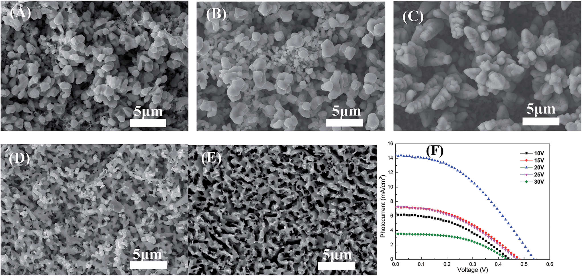 | ||
| Fig. 7 SEM images at different etching voltages (A) 10 V, (B) 15 V, (C) 20 V, (D) 25 V, (E) 25 V and (F) J–V curves obtained based on different voltages. | ||
EIS was used to investigate the charge transfer resistance (Rct), which is related to the electrocatalytic activity of the different CEs. Fig. 8(A) shows Nyquist plots of the QDSCs using Cu1.8S/CuS, Cu2S and Pt CEs. The charge transfer resistance, Rct, corresponding to charge exchange between the different counter electrodes and the polysulfide electrolyte is derived from the semi arcs in the Nyquist plots. For Pt, Rct is very large, about 3212 Ω, demonstrating sluggish kinetics. This is further attested by no evident diffusion component in the Nyquist plot. Rct for Cu2S is about 43.05 Ω, which is much smaller than that for Pt. In addition, Cu1.8S/CuS exhibits a smaller value of 5.18 Ω. Note that an efficient QDSSC usually exhibits a low Rct value.20 From the J–V and Table 1, the electrocatalytic activity in polysulfide electrolyte are in the order, Cu1.8S/CuS > Cu2S > Pt, which is consistent with the Rct results obtained from EIS. The inset in Fig. 8(A) shows that Rs for Pt is 3.52 Ω, which is much larger than that for Cu2S (Rs = 2.82 Ω) and Cu1.8S/CuS (Rs = 1.23 Ω). QDSC with an electrode with a greater Rs value provides smaller Jsc values.17 From Table 1, Cu1.8S/CuS exhibited a Jsc value of 14.50 mA cm−2, which was much larger than the Pt CE (4.40 mA cm−2) and Cu2S CE (8.13 mA cm−2). These results prove that the smaller Rct and Rs of Cu1.8S/CuS CE show lower charge transfer resistance and superior electrocatalytic activity.
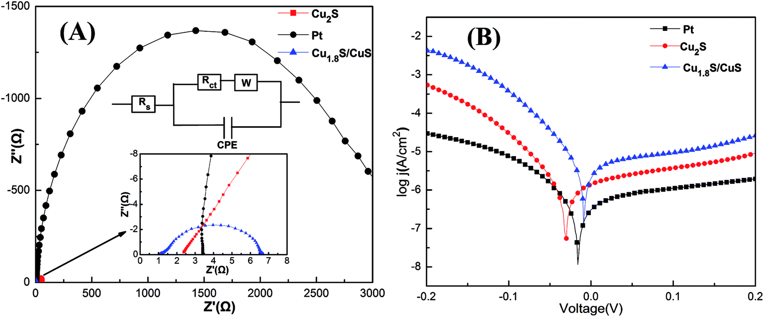 | ||
| Fig. 8 (A) Nyquist plots and (B) Tafel polarization of the symmetrical dummy cells based on Pt, Cu2S and Cu1.8S/CuS CEs. The inset in (A) shows the equivalent circuit used for fitting the impedance spectroscopy, in which Rs represents the series resistance, Rct and CPE represents the charge-transfer resistance and the corresponding constant phase angle element at the CE/electrolyte interface, and W is the Warburg diffusion impedance of the electrolyte.10,28,29 | ||
Based on the EIS results, it should be expected that Cu1.8S/CuS exhibits much higher photoelectrochemical performance than Pt and Cu2S. Therefore, theoretical calculations and Tafel polarization measurements were further carried out in the dummy cell used in the EIS experiments to prove this. It is known that the exchange current density (J0), which is equal to J0 = RT/nFRct,30 is directly related to the electrochemical catalytic activity of the electrode, where R is the gas constant, T is the absolute temperature in K, n is the number of electrons involved in the electrochemical reduction reaction, F is the Faraday constant, and Rct is the charge transfer resistance.31 From EIS, Rct are in a consistent order of Cu1.8S/CuS < Cu2S < Pt, so we can obtain the exchange current density (J0) in a consistent order of Pt < Cu2S < Cu1.8S/CuS by theoretical calculations. At the same time, Fig. 8(B) shows the logarithmic current density (logJ) as a function of the voltage (V) for the oxidation/reduction of the S2−/Sn2− couple. The exchange current densities (J0), which can be estimated from the extrapolated intercepts of the cathodic branches of the corresponding Tafel plots, are in a consistent order of Pt < Cu2S < Cu1.8S/CuS. These results confirm that electroactive materials with a higher exchange current density require a lower activation energy, and it is much easier for Cu1.8S/CuS to catalyze the reduction of S2−/Sn2−. EIS, J–V curves of QDSCs and Tafel polarization show good consistency with the corresponding photovoltaic performance of QDSC devices based on different CEs, in which the QDSCs based on Cu1.8S/CuS CE shows the highest performance.
4. Conclusion
In this study, we demonstrated that Cu1.8S/CuS as CE exhibits excellent electrochemical catalyze activity and remarkable stability in catalyzing the reduction of Sn2− to S2−. The photoelectrochemical performance of QDSCs based on Cu1.8S/CuS CE (ff = 0.41 and η = 3.22%) was much higher than that of Pt and Cu2S CEs. At the same time, it is a simple and efficient method for fabricating nanoplates based on the Cu micro-nanostructure by the AC etching of brass. Our results show that the Cu1.8S/CuS CE can be suitable for replacing the most expensive Pt CE and other copper sulfide electrodes derived from copper and brass sheets.Acknowledgements
Funding of this research by national science foundation of China (grant no. 51371020) is gratefully acknowledgment.References
- B. O'regan and M. Grfitzeli, Nature, 1991, 353, 737–740 CrossRef.
- W. Lee, S. K. Min, V. Dhas and S. H. Han, Electrochem. Commun., 2009, 11, 103–106 CrossRef CAS PubMed.
- S. S. Kalanur, S. Y. Chae and O. S. Joo, Electrochim. Acta, 2013, 103, 91–95 CrossRef CAS PubMed.
- Y. L. Lee, B. M. Huang and H. T. Chien, Chem. Mater., 2008, 20, 6903–6905 CrossRef CAS.
- H. J. Lee, et al, Langmuir, 2009, 25, 7602–7608 CrossRef CAS PubMed.
- L. E. Brus, J. Chem. Phys., 1984, 80, 4403 CrossRef CAS PubMed.
- Z. Lou, J. Deng, L. Wang, R. Wang, T. Fei and T. Zhang, RSC Adv., 2013, 3, 3131–3136 RSC.
- F. Zhu, D. Wu, Q. Li, H. Dong, J. Li, K. Jiang and D. Xu, RSC Adv., 2012, 2, 11629–11637 RSC.
- A. Nozik, Phys. E, 2002, 14, 115–120 CrossRef CAS.
- G. R. Li, J. Song, G. L. Pan and X. P. Gao, Energy Environ. Sci., 2011, 4, 1680–1683 CAS.
- A. Yella, et al, Science, 2011, 334, 629–634 CrossRef CAS PubMed.
- Z. S. Yang, C. Y. Chen, C. W. Liu and H. T. Chang, Chem. Commun., 2010, 46, 5485–5487 RSC.
- I. Mora-Seró, S. Giménez, F. Fabregat-Santiago, R. Gómez, Q. Shen, T. Toyoda and J. Bisquert, Acc. Chem. Res., 2009, 42, 1848–1857 CrossRef PubMed.
- G. Hodes, J. Manassen and D. Cahen, J. Electrochem. Soc., 1980, 127, 544–549 CrossRef CAS PubMed.
- Z. Tachan, M. Shalom, I. Hod, S. Rühle, S. Tirosh and A. Zaban, J. Phys. Chem. C, 2011, 115, 6162–6166 CAS.
- C.-Y. Lin, C.-Y. Teng, T.-L. Li, Y.-L. Lee and H. Teng, J. Mater. Chem. A, 2013, 1, 1155–1162 CAS.
- Z. S. Yang, C. Y. Chen, C. W. Liu, C. L. Li and H. T. Chang, Adv. Energy Mater., 2011, 1, 259–264 CrossRef CAS.
- J. G. Radich, R. Dwyer and P. V. Kamat, J. Phys. Chem., 2011, 2, 2453–2460 CAS.
- H. Chen, L. Zhu, H. Liu and W. Li, J. Power Sources, 2014, 245, 406–410 CrossRef CAS PubMed.
- A. Hauch and A. Georg, Electrochim. Acta, 2001, 46, 3457–3466 CrossRef CAS.
- H. Chen, W. Li, H. Liu and L. Zhu, Microporous Mesoporous Mater., 2011, 138, 235–238 CrossRef CAS PubMed.
- Z. Wang, L. Zhu, W. Li, H. Xu and H. Liu, Surf. Coat. Technol., 2013, 235, 290–296 CrossRef CAS PubMed.
- H. Chen, L. Zhu, H. Liu and W. Li, J. Phys. Chem. C, 2013, 117, 3739–3746 CAS.
- M. H. Deng, Q. X. Zhang, S. Q. Huang, D. M. Li, Y. H. Luo, Q. Shen, T. Toyoda and Q. B. Meng, Nanoscale Res. Lett., 2010, 5, 986–990 CrossRef CAS PubMed.
- Y. Jiang, X. Zhang, Q. Q. Ge, B. B. Yu, Y. G. Zou, W. J. Jiang, W. G. Song, L. J. Wan and J. S. Hu, Nano Lett., 2014, 14, 365–372 CrossRef CAS PubMed.
- H. Salaramoli, E. Maleki, Z. Shariatinia and M. Ranjbar, J. Photochem. Photobiol., A, 2013, 271, 56–64 CrossRef CAS PubMed.
- J. G. Chen, H. Y. Wei and K. C. Ho, Sol. Energy Mater. Sol. Cells, 2007, 91, 1472–1477 CrossRef CAS PubMed.
- S. Giménez, I. Mora-Seró, L. Macor, N. Guijarro, T. Lana-Villarreal, R. Gómez, L. J. Diguna, Q. Shen, T. Toyoda and J. Bisquert, Nanotechnology, 2009, 20, 295204 CrossRef PubMed.
- X. Xin, M. He, W. Han, J. Jung and Z. Lin, Angew. Chem., Int. Ed., 2011, 50, 11739–11742 CrossRef CAS PubMed.
- M. K. Wang, A. M. Anghel, B. Marsan, N. C. Ha, N. Pootrakulchote, S. M. Zakeeruddin and M. Grätzel, J. Am. Chem. Soc., 2009, 131, 15976–15977 CrossRef CAS PubMed.
- Y. C. Wang, D. Y. Wang, Y. T. Jiang, H. A. Chen, C. C. Chen, K. C. Ho, H. L. Chou and C. W. Chen, Angew. Chem., Int. Ed., 2013, 52, 6694–6698 CrossRef CAS PubMed.
| This journal is © The Royal Society of Chemistry 2014 |