
 Open Access Article
 This Open Access Article is licensed under a Creative Commons Attribution-Non Commercial 3.0 Unported Licence
Novel broadband Cr4+:YAG chip fabricated by sol–gel technique for optical amplifiers
Kai-Chieh Chang *a,
Yu-Hao Chenc,
Chien-Wei Huangc,
Chun-Nien Liu*b,
Sheng-Lung Huanga and
Wood-Hi Chengd
*a,
Yu-Hao Chenc,
Chien-Wei Huangc,
Chun-Nien Liu*b,
Sheng-Lung Huanga and
Wood-Hi Chengd
aThe Graduate Institute of Photonics and Optoelectronics, National Taiwan University, Taipei 102, Taiwan. E-mail: chang3175@gmail.com
bThe Department of Electrical Engineering, National Chung Hsing University, Taichung, 402, Taiwan. E-mail: terbovine@email.nchu.edu.tw
cThe Graduates Institute of Optoelectronic Engineering, National Chung Hsing University, Taichung 402, Taiwan
dDepartment of Electrical Engineering, National Chun Hsing University, Taichung, 402, Taiwan
First published on 13th May 2025
Abstract
We introduce a novel Cr4+:YAG waveguide, fabricated using the sol–gel technique, as a potential game-changer in high-speed optical communication. This waveguide, a strong candidate for a broadband fiber amplifier covering the interval from 1.3 μm to 1.6 μm, is fabricated on a coat-etched microchannel quartz substrate. The waveguide's fluorescence spectrum is centered at 1550 nm, boasting a gain measurement of 1.2 dB. These waveguide chips, with their exciting potential for integration into silicon photonic chips, are positioned to bring about significant advancements in high-speed optical communication applications.
1. Introduction
Optical communication has seen rapid growth in recent years, driven by the dramatic increase in demand for high-performance optical networks. However, current optical communications systems that rely heavily on doped fiber amplifiers (EDFAs) are not without limitations. These systems have a limited bandwidth of 70 nm and are large, requiring a certain length to provide sufficient gain. These limitations may prevent future user needs from being met. A viable alternative has been proposed to address this pressing challenge: chromium-doped fiber amplifiers (CDFAs).1The rapid development of today's optical communication technology has increased demand for high-capacity and long-distance transmission. In visual communications, fiber amplifiers are widely used for signal enhancement to improve transmission distance and increase signal quality. However, conventional fiber amplifiers have some limitations, such as requiring more space, further limiting their performance in more demanding applications. To achieve smaller sizes and higher integration, which saves space and improves performance, the optical waveguide structures with the integration of silicon photonic chips are essential.2–4
Silicon photonics is a CMOS process that integrates numerous optical components into a miniature silicon chip. However, the material properties of the silicon base are not suitable for making light sources and optical amplifiers, and it will always be a challenge to match silicon photonics chips. The success of EDFAs in the past has led to significant growth in the global optical communications market.5 In-depth studies have examined Er-doped waveguide amplifier (EDWA) components, and they actively employ these components in data centers for long-distance data transmission in the C + L band. The research on rare earth ion optical waveguide amplifiers for low dispersion O-band is relatively limited. Therefore, applying heat treatment and co-doping technologies to develop low-dispersion, high-gain-doped silicon photonic chips6 for high-speed optical communication applications may have academic foresight and industrial value since the gain spectrum of doped chromium materials is around 1200–1600 nm. This includes the 1310 nm band for low dispersion and the 1550 nm band for low-loss optical communication applications.
Recent research has indicated the CDFA provides a bandwidth that is 4.3 times broader than that of EDFA.7–9 The excited chromium ions to emit photons within the 1200 to 1600 nm range provided an adequate covering of the critical optical communication bands (C, L, O bands) at 1310 nm with low dispersion and 1550 nm with low loss.10
To date, several synthesis methods for Cr4+:YAG have been explored, yet each presents distinct challenges. For instance, co-precipitation11 and spray pyrolysis12 often require excessively high sintering temperatures (e.g., >1400 °C for Ce:YAG12), which escalate production costs and induce thermal stress. Hydrothermal synthesis, as demonstrated in Tb:YAG fabrication,13 demands stringent control over pH and ion concentration, with elevated temperatures paradoxically reducing metal oxide solubility and compromising sample homogeneity. Citrate-gel methods,14 while enabling crystallization at 800 °C for Eu:YAG, are sensitive to initial pH and citrate content—parameters incompatible with chromium doping. Nitrate–citrate sol–gel combustion15 broadens the sintering window (800 °C to 1200 °C) but necessitates prolonged durations (>2 hours), contrasting sharply with our 15 minute crystallization at 950 °C. These limitations hinder commercial viability due to energy inefficiency, process complexity, or extended fabrication timelines.
In this study, we propose the fabrication of Cr4+:YAG waveguides using the sol–gel method, which demonstrates significant innovations and originality. First, the process operates at a lower temperature range, reduced from the conventional16 1200 °C to 900 °C. Based on Thermogravimetric Analyzer (TGA) measurements showing a crystallization point at 930 °C and observed cladding layer cracking due to thermal stress above 1100 °C, the annealing temperature was strategically set at 1000 °C. This approach achieves both energy efficiency and minimized thermal impact on the material. Second, the fabricated waveguides exhibit remarkably low impurity content of only 2%, accompanied by enhanced optical performance. Third, the manufacturing duration has been substantially shortened from 12 hours to merely 6 hours, significantly improving production efficiency.17,18
Subsequently, we apply this Cr4+:YAG waveguide as a coating on etched microchannel quartz substrates to generate an optical amplification chip waveguide. These waveguides are expected to play a crucial role in fabricating chromium-doped optical waveguides on silicon wafers, providing a novel solution for next-generation optical amplifiers that aim to overcome the bandwidth limitations currently faced by EDFA-based systems.
Our research will be applied to optical communications and extended to the manufacture of waveguide lasers. Chromium-doped materials can be used to realize broadband, high-efficiency light amplification, thereby enhancing the performance and application of lasers. In addition, in the field of optical sensing, chromium-doped waveguide materials can be used to develop high-sensitivity, high-precision optical sensors for applications such as environmental monitoring and industrial control.
2. Fabrication
Cr4+:YAG waveguides were prepared by hydrolysis, condensation, and gelation of aluminum isopropoxide mixed with chromium and chlorides yttrium in isopropanol, known as the sol–gel method.19 First, we designed two solutions: solution A, consisting of yttrium chloride anhydrous and chromium chloride hexahydrate dissolved in isopropanol, and solution B, consisting of potassium metal dissolved in isopropanol. The waveguide synthesized parameters are shown in Table 1.| Concentration | YCl3 | CrCl3·6H2O | K | C9H21O3Al |
|---|---|---|---|---|
| 3% | 4 g | 0.14 g | 2.45 g | 6.73 g |
| 6% | 4 g | 0.28 g | 2.52 g | 6.51 g |
| 9% | 4 g | 0.42 g | 2.58 g | 6.34 g |
| 12% | 4 g | 0.56 g | 2.65 g | 6.13 g |
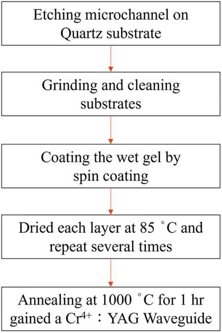
These two solutions were mixed with vigorous stirring and refluxed at 85 °C for one hour, and then a powder of aluminum isopropoxide was added directly to the previous solution. Then, these two solutions were refluxed at 85 °C, and a homogeneous solution was obtained with vigorous stirring for 4 hours. After cooling, we utilized a centrifuge to separate potassium chloride, resulting in a clear solution. A white sol was formed through direct hydrolysis by adding deionized water. A flow chart of the Cr4+:YAG waveguide fabrication is shown in Fig. 1.
 | ||
| Fig. 1 Flow chart of sol–gel method. | ||
Temperature-resistant SiO2 (up to 1100 °C) was selected as the substrate material. The waveguide was designed to operate in single-mode to minimize optical transmission loss. To ensure a normalized frequency (V-number) below 2.405, the ideal waveguide numerical aperture (NA) must be less than 0.138. However, due to limitations in current photomask fabrication and lithography/exposure techniques, the minimum achievable linewidth is restricted to 4 μm to 5 μm. Therefore, our goal was to fabricate waveguides as close to the ideal width as possible while adhering to equipment constraints. Ultimately, a waveguide with a 4.3 μm linewidth was etched. Subsequently, to ensure smooth waveguide end-faces, we performed sequential grinding (using grit sizes from 25 μm down to 3 μm) followed by polishing with a 1 μm polishing slurry. For the thin-film coating, a sol–gel solution was applied to the quartz substrate via spin coating. The substrate was mounted on a spin coater, and the sol–gel solution was dispensed onto its surface. Spin coating was conducted at 4000 rpm for 10 seconds. After each coating layer, the substrate was dried at 85 °C for 5 minutes. This process was repeated to achieve multilayer coatings, with the thin-film deposition workflow illustrated in Fig. 2. Finally, the substrate underwent annealing at 1000 °C for 1 hour. The sample results are shown in Fig. 3.
 | ||
| Fig. 2 Flow chart of thin film coating. | ||
 | ||
| Fig. 3 OCT image of the surface structure of Cr4+:YAG waveguide. | ||
3. Measurements and results
3.1 Thermogravimetric analyzer (TGA)
To obtain a quality sample, the sample processes are facilized heating by oxidation, pyrolysis, and evaporation. These processes will allow us to understand the sample's thermal properties, the sample analysis's composition, and other important information.A microbalance process was used to make the dry gel sample, and the sample was heated to the set temperature within an environment that maintained a constant temperature. The thermogravimetric analyser is employed to measure the weight of the sample and record data.
Fig. 4 shows a thermogravimetric analyser (TGA) plot of dry gel sample mass versus temperature. We observed a progressive decrease in the dry gel's mass as the temperature gradually rose from room temperature (30 °C). This reduction is attributed to the increasing temperature-inducing pyrolysis in various organic substances within the sample. As the temperature reaches 930 °C, the curve gradually flattens, signifying the decomposition of the organic material in the sample. The temperature at 930 °C indicated the crystallization temperature of the samples enabled to confirm the minimum sintering temperature required for the process.
 | ||
| Fig. 4 TGA plot of dry gel sample mass versus temperature. | ||
3.2 High-resolution X-ray diffractometer (HRXRD)
This study uses a high-resolution X-ray diffractometer (HRXRD) to analyse materials' crystalline structure and quality and provide critical crystallization-related data. X-ray diffractometer (XRD) utilizes the principle of light–crystal interaction and explains the phenomenon of interaction between X-rays and crystal structure by applying Bragg's law in eqn (1), where n represents the number of passes, λ is the wavelength of X-rays, d is the distance between lattice planes, and θ is the detection angle.
2d![[thin space (1/6-em)]](https://www.rsc.org/images/entities/char_2009.gif) sinθ = nλ sinθ = nλ
| (1) |
To verify whether Cr4+:YAG can be synthesized by the sol–gel method, we measured the crystalline state of the synthesized sample (Cr4+:YAG powder with 3% doping concentration) by using an X-ray winding diffraction analyser, and the results are shown in Fig. 5. In Fig. 5, the YAG powder scattered the energy at various angles to produce the scattering peak after X-ray irradiation. A peak of 99% intensity at the angle of 33.3173° (2-theta) was observed. This matched the peaks of the JCPD card references in the Fig. 5. It indicates that the sol–gel method can indeed synthesize the YAG lattice.
 | ||
| Fig. 5 XRD measurement of Cr4+:YAG powder with 3% doping concentration. | ||
After confirming that YAG crystals can be synthesized by this method, we made chromium doping ratios of 3%, 6%, 9%, and 12% to verify that YAG crystals can be synthesized at different doping concentrations. We measured the XRD, which showed that YAG crystals can be formed regardless of the doping concentration. Fig. 6 shows the thin film diffraction pattern with different chromium doping concentrations of Cr4+:YAG from 3% to 12%. A peak intensity at the angle of 33.3173° was observed, like Fig. 5.
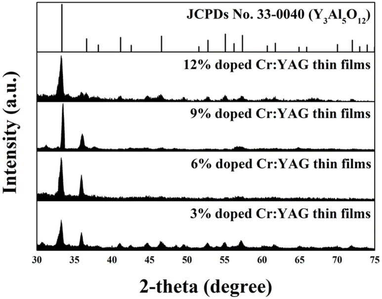 | ||
| Fig. 6 Thin film diffraction pattern with different chromium doping concentrations. | ||
3.3 Scanning electron microscope (SEM)
After confirming the YAG was successfully synthesized and crystallized by the XRD, we conducted elemental analysis of the samples through field emission scanning electron microscopy (FESEM) and high-resolution electron microprobe (HREM) to verify the impurities of the synthesized samples. Fig. 7 shows the results of the elemental analysis of Cr4+:YAG powder by energy-dispersive X-ray spectroscopy (EDS) in SEM. We observed no excessive impurities in the synthesized powder samples except for the carbon-coated before measurement. Table 2 shows the impurity content.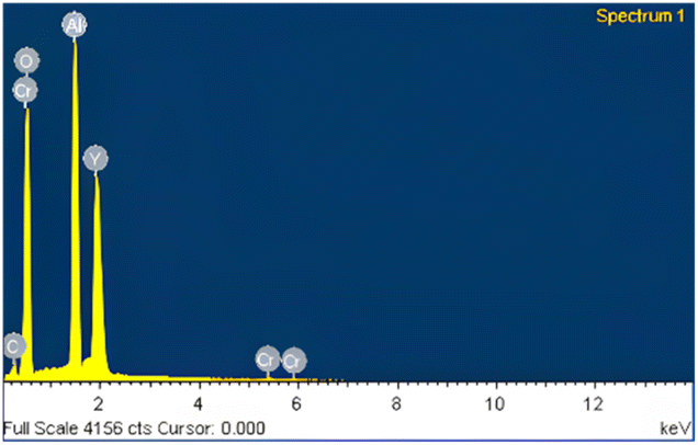 | ||
| Fig. 7 EDS analysis of Cr4+:YAG powder. | ||
| Element | Percentage (%) |
|---|---|
| Yttrium (Y) | 42.62 |
| Oxygen (O) | 32.18 |
| Aluminum (Al) | 19.29 |
| Chromium (Cr) | 2.56 |
| Chlorine (Cl) | 0.69 |
| Carbon (C) | 0.25 |
| Silicon (Si) | 1.21 |
| Iron (Fe) | 0.28 |
3.4 The fluorescence spectrum of Cr4+:YAG waveguide
A photoluminescence (PL) was used to measure the fluorescence. The wavelength of the excitation laser was 1064 nm. We detected a fluorescence spectrum with a center wavelength of about 1400 nm from each doping concentration absorbed the excitation light. The result was consistent with the spectrum of chromium ions from the commercial rods in the literature, as shown in Fig. 8. This indicated that we had successfully doped our sample with Cr4+ ions. The fluorescence intensity was observed to increase with higher concentrations of Cr4+ ions, indicating successful doping and enhanced photoluminescence efficiency. | ||
| Fig. 8 Fluorescence spectra of Cr4+:YAG thin films with different doping concentrations. | ||
Fig. 9 shows the setting of the fluorescence characteristic measurement. The 1064 nm excitation laser and the 1550 nm tunable laser were first combined using a WDM coupler. The output fiber from the WDM (Wavelength Division Multiplexer) coupler was then precisely aligned with the input facet of the Cr4+:YAG waveguide using a high-precision translation stage to ensure efficient optical coupling. This setup enables both wavelengths to be simultaneously injected into the waveguide, allowing effective interaction within the chromium-doped region. The back end of the waveguide receives the signal via a multimode fiber, which is then connected to an optical spectrum analyser (OSA) to record the measurements.
 | ||
| Fig. 9 Setup of the fluorescence characteristic measurement. | ||
3.5 Measurement of waveguide transmission characteristics
After the measurement of fluorescence characteristics and gain, it was confirmed that the Cr4+:YAG waveguide has gain effect, and finally, the transmission mode was analysed and measured to confirm the transmission capability of the samples. The structure of the measurement is shown in Fig. 10, where a laser with a wavelength of 1550 nm is used to couple the laser source into the doped YAG waveguide, a wavefront measuring device is used to analyse the light gain, and the distance between the wavefront measuring device and the doped YAG waveguide is gradually increased to obtain the far-field analysis graphs at different distances, as shown in Fig. 11.|
NA = n0sin(αmax(θ))
| (2) |
| V = 2πa/λ × NA | (3) |
 | ||
| Fig. 10 Setup of the transmission characteristics measurement. | ||
 | ||
| Fig. 11 Measurement results of different intervals of mold field pattern. | ||
According to the far-field azimuthal patterns shown in Fig. 10 at different distances, the angle (αmax(θ)) is calculated as 7.5056° using Fig. 12, with N0 = 1 (air). Applying eqn (2), the numerical aperture (NA) is determined to be approximately 0.1306. Based on this NA value, with a core radius a = 4.3 μm and a wavelength of 1.55 μm, the calculated V-number using eqn (3) is 2.275, which is below the cut-off value of 2.405. This confirms that the transmission mode operates in single-mode.
 | ||
| Fig. 12 Angle αmax(θ) calculation flow and schematic diagram. | ||
To further enhance transmission efficiency, minimizing the insertion loss of the waveguide is fundamental to manufacturing high-quality waveguides. Fig. 13 illustrates the structure, where the insertion loss consists of surface loss and waveguide transmission loss. The results, shown in Fig. 14, indicate a unit length loss of 0.2 dB mm−1 and a total loss of 4 dB at a wavelength of 1550 nm.
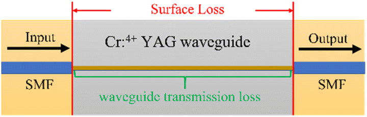 | ||
| Fig. 13 Flow chart of device structure. | ||
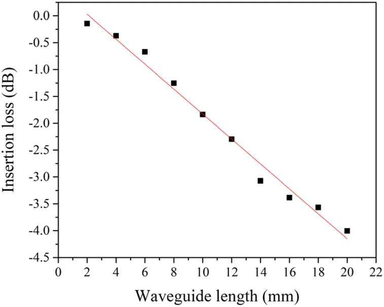 | ||
| Fig. 14 Relationship between the insertion loss and the waveguide length. | ||
3.6 The net gain of Cr4+:YAG waveguide
The net gain is defined as the total optical gain minus the aggregate losses, including coupling, scattering, and absorption losses in the chromium-doped crystal waveguide (CCW).20,21 The experimental setup, as illustrated in Fig. 9, employed a 1064 nm Yb doped fiber laser pump source and a 1550 nm signal source with 0.3 mW output power, complemented by a polarization controller. The optical amplification of the CCW signal was quantified using a spectrum analyzer.At 1550 nm wavelength with a 20 mm waveguide length, the measured total loss reached 4 dB, corresponding to a linear loss coefficient of 0.2 dB mm−1.
Fig. 15, demonstrates the critical correlation between pump power and net gain performance. Below the threshold pump power range (50 mW to 100 mW), losses dominate the system characteristics, resulting in near-zero net gain. Beyond this threshold, pump energy efficiently excites chromium ions to their metastable states, inducing significant gain enhancement. At elevated pump powers, excited-state population approaches saturation limits, leading to gain saturation. The maximum net gain of 1.2 dB was achieved by subtracting the total loss (4 dB) from the peak total gain (5.2 dB) under optimized pumping conditions.
 | ||
| Fig. 15 Net gain as a function of pumping power of Cr4+:YAG thin films. | ||
As shown in Fig. 16, this study investigates the relationship between the number of thin-film layers and net gain. The experiment employed a multilayer thin-film structure with each layer measuring 100 nm in thickness, and the total number of layers was set to 50. This upper limit was primarily determined by process constraints: when the waveguide groove etching depth exceeds 5 μm (corresponding to 50 layers), photoresist materials cannot withstand prolonged high-temperature exposure, leading to structural deformation of the waveguide. Furthermore, the research revealed significant optical performance dependencies on film thickness parameters. Insufficient total film thickness resulted in increased surface roughness after thermal annealing treatment, thereby elevating light scattering losses. More critically, when the total film thickness fell below the incident laser spot size, substantial reductions in optical coupling efficiency and laser power output were observed. These combined effects amplified overall transmission losses, ultimately resulting in diminished net gain.
 | ||
| Fig. 16 The relationship between the number of thin-film layers and net gain. | ||
4. Discussion and conclusion
This study successfully synthesized Cr4+:YAG crystals using the sol–gel method. Their crystallinity was confirmed by X-ray diffraction (XRD) analysis, exhibiting a characteristic peak at approximately 2θ = 33.317°. Waveguides were subsequently fabricated by spin-coating the precursor wet gel onto quartz substrates. Both XRD and Energy Dispersive X-ray Spectroscopy (EDS) measurements verified the high purity of the prepared samples.Preliminary fluorescence characterization indicated that the fabricated waveguides exhibit a gain of 1.2 dB, with a central emission wavelength centered around 1550 nm. However, to meet the requirements for optical amplifier applications, further optimization of the waveguide design and fabrication process is necessary to achieve higher gain. Research addressing this is currently underway.
Building upon this work, future efforts will focus on developing low-dispersion, high-gain chromium-doped silicon photonic waveguide chips utilizing co-doping techniques. Given the broad gain spectrum of chromium-doped materials (1200 nm to 1600 nm), they are particularly well-suited for high-speed optical communication applications within the low-dispersion O-band (1260 nm to 1360 nm). This research direction holds significant potential for both academic advancement and industrial application.
Data availability
All data that support the findings of this study are included within the article.Conflicts of interest
There are no conflicts to declare.Acknowledgements
This work was partially supported by the Ministry of Science and Technology, Taiwan (MOST) (111RB02, 110RB02, 110-2622-E-005-010, 109-2218-E-005-012, 109-2823-8-005-003, and 108-2218-E-005-018). And Ministry of Education, Taiwan (MOE) (111RA077A and 110RA077A).Notes and references
- C.-N. Liu, et al., Record 22-dB Net Gain of Broadband Single-Mode Cr-Doped Crystalline Core Fiber by AI-Assisted Image Recognition Growth, J. Lightwave Technol., 2023, 42(8), 2971–2977 Search PubMed.
- C. Kopp, et al., Silicon photonic circuits: on-CMOS integration, fiber optical coupling, and packaging, IEEE J. Sel. Top. Quantum Electron., 2010, 17(3), 498–509 Search PubMed.
- C. L. Canedy, et al., Mid-infrared interband cascade light emitting devices grown on off-axis silicon substrates, Opt. Express, 2021, 29(22), 35426–35441 Search PubMed.
- S. Hadzialic, et al., Two-dimensional photonic crystals fabricated in monolithic single-crystal silicon, IEEE Photonics Technol. Lett., 2009, 22(2), 67–69 Search PubMed.
- S. Y. Siew, et al., Review of silicon photonics technology and platform development, J. Lightwave Technol., 2021, 39(13), 4374–4389 Search PubMed.
- Z. Chen, et al., On-chip waveguide amplifiers for multi-band optical communications: a review and challenge, J. Lightwave Technol., 2022, 40(11), 3364–3373 Search PubMed.
- K.-C. Chang and et al., Gain Enhancement of Broadband Single-Mode Cr-Doped Fibers Employing Thermal Annealing, 2018 23rd Opto-Electronics and Communications Conference (OECC), IEEE, 2018 Search PubMed.
- C.-M. Liu and et al., Tetrahedral-Cr enhancement employing dielectric coating for higher gain of broadband Cr-doped fiber amplifiers, Optical Fiber Communication Conference, Optica Publishing Group, 2020 Search PubMed.
- K.-C. Chang and et al., Record gain of 300-nm broadband single-model Cr-doped crystalline fiber employing novel growth of smaller core, Next-Generation Optical Communication: Components, Sub-Systems, and Systems XI, SPIE, vol. 12028, 2022 Search PubMed.
- C.-N. Liu, et al., Higher-Gain Broadband Single-Mode Chromium-Doped Fiber Amplifiers by Tetrahedral-Chromium Enhancement, 2019 Optical Fiber Communications Conference and Exhibition (OFC), 2019, pp. 1–3 Search PubMed.
- H. Wang, L. Gao and K. Niihara, Synthesis of nanoscaled yttrium aluminum garnet powder by the co-precipitation method, J. Mater. Sci. Eng. A, 2000, 288(1), 1–4 Search PubMed.
- Y. C. Kang, et al., Photoluminescence characteristics of YAG:Tb phosphor particles with spherical morphology and non-aggregation, J. Phys. Chem. Solids, 1999, 60(11), 1855–1858 Search PubMed.
- Y. Hakuta, et al., Continuous production of phosphor YAG:Tb nanoparticles by hydrothermal synthesis in supercritical water, Mater. Res. Bull., 2003, 38(7), 1257–1265 Search PubMed.
- Y. H. Zhou, et al., Preparation of Y3Al5O12:Eu phosphors by citric–gel method and their luminescent properties, Opt. Mater., 2002, 20(1), 13–20 Search PubMed.
- X. Chen, et al., Fabrication and photoluminescence properties of Cr:YAG and Yb, Cr:YAG transparent ceramic, Opt. Mater., 2015, 49, 330–336 Search PubMed.
- R. S. Pugina, et al., Nd3+:YAG microspheres powders prepared by spray pyrolysis: synthesis, characterization and random laser application, Mater. Chem. Phys., 2021, 269, 124764 Search PubMed.
- E. R. Kupp, et al., Particle size effects on yttrium aluminum garnet (YAG) phase formation by solid-state reaction, J. Mater. Res., 2014, 29(19), 2303–2311 Search PubMed.
- A. Potdevin, et al., Sol–gel based YAG: Tb3+ or Eu3+ phosphors for application in lighting sources, J. Phys. D: Appl. Phys., 2005, 38(17), 3251 Search PubMed.
- Y. Li and R. M. Almeida, Preparation and optical properties of sol–gel derived thick YAG:Ce3+ phosphor film, Opt. Mater., 2012, 34, 1148–1154 Search PubMed.
- C.-N. Liu, et al., Broadband single-mode Cr-doped crystalline core fiber with record 11-dB net gain by precise laser-heated pedestal growth and tetrahedral chromium optimization, J. Lightwave Technol., 2021, 39(11), 3531–3538 Search PubMed.
- V. Kartazaev and R. R. Alfano, Polarization influence of excited state absorption on the performance of Cr4+:YAG laser, Opt. Commun., 2004, 242(4–6), 605–611 Search PubMed.
| This journal is © The Royal Society of Chemistry 2025 |