
 Open Access Article
 This Open Access Article is licensed under a
 Creative Commons Attribution 3.0 Unported Licence
Length-independent charge transport of well-separated single-crystal TiO2 long nanowire arrays†
Jie
Liu
,
Xia
Sheng
,
Fengying
Guan
,
Ke
Li
,
Dandan
Wang
,
Liping
Chen
and
Xinjian
Feng
 *
*
College of Chemistry, Chemical Engineering and Materials Science, Soochow University, Suzhou 215123, China. E-mail: xjfeng@suda.edu.cn
First published on 6th August 2018
Abstract
Long, well-separated single crystal TiO2 nanowire (NW) arrays with rapid charge transport properties hold great promise in photoelectrochemical and energy storage devices. Synthesis variations to increase the NWs length generally result in the widening of the NWs and fusion at their roots which, in turn, increases the structural disorder and slows charge transport. As such, well-separated single-crystal TiO2 NW arrays with rapid charge transport properties have been limited to lengths of about 3–4 μm. In this work, by adjusting the HCl/DI-water ratio and adding specific organic ligands to the reaction solution that slow the lateral growth rate we achieve well-separated single-crystal rutile TiO2 NW arrays with a length of ∼10 μm and an aspect ratio of approximately 100. The charge transport is 100 times faster than that of nanoparticle films and remarkably exhibits length-independence, a behavior that can be attributed to the well-separated architecture. The synthesis strategy can be extended to the fabrication of other well-separated metal oxide NW arrays and represents an important tool in achieving high performance photoelectrochemical and electrical energy storage devices.
Introduction
Vertically aligned semiconductor nanowire (NW) arrays have attracted great attention due to their unique optical and electronic properties.1–8 Recent work on well-separated single-crystal rutile TiO2 NW arrays has shown that the electron diffusion coefficient is two orders of magnitude higher than that in mesoporous films comprised of randomly packed nanoparticles (NPs), corresponding to an electron diffusion length of about 60 μm9 and offering the promise of useful application of long NW arrays within devices such as solar cells, photodetectors, and chemical sensors.10–13 However, the synthesis of well-separated rutile TiO2 NW arrays has been limited to lengths of about 3–4 μm.7,14,15 During the conventional bottom-up growth process, synthesis variations to increase the length generally result in the widening of the NWs and subsequent fusion at their roots.16–18 This, in turn, reduces the aspect ratio, increases the structural disorder and reduces the charge transport;19,20 experimental results shown in ESI Fig. S1† indicate that the diffusion coefficient of bundled TiO2 NWs is over one order of magnitude lower than that of well-separated ones. To date, the growth of long and well-separated single-crystal rutile TiO2 NW arrays has remained an unmet challenge.Herein, by suppressing NW lateral growth, we report the one-step synthesis of well-separated single-crystal rutile TiO2 NW arrays with a length of ∼10 μm having an aspect ratio of approximately 100, a value over 5 times greater than previously reported.7 Not only is electron transport in these NW arrays 100 times faster than in NP films, but charge collection efficiency is found to be independent of length. We believe that the well separated long single-crystal TiO2 NW arrays can facilitate the development of a broad range of photovoltaic and photoelectrochemical devices.
Results and discussion
Characterization of TiO2 NW arrays
Aligned well-separated ∼10 μm long single-crystal rutile TiO2 NW arrays were prepared via a facile solvothermal method. In a typical experiment, a FTO coated glass substrate supporting a TiO2 seed layer was loaded into a Teflon-lined stainless-steel reactor (23 mL) filled with a reaction solution composed of 2-butanone, ethanol, hydrochloric acid (HCl, 37%) and titanium butoxide (TBOT). The reaction temperature was set at 443 K for variable durations. Fig. 1a and b are typical field emission scanning electron microscope (FE-SEM) images of the NWs obtained after a reaction time of 4.5 h. The NWs have an average length of ∼10 μm, 98–105 nm diameters, and an aspect ratio of ∼100, and are well separated over their entire length. From X-ray diffraction (XRD), see Fig. S2,† the crystal phase of the NWs can be identified as tetragonal rutile (JCPDS no. 21-1276). The (002) diffraction peak is much stronger than the other peaks, suggesting that the NWs have a preferred [001] growth direction. Fig. 1c is a transmission electron microscopy (TEM) image of a typical NW. The high-resolution TEM image shown in the inset of Fig. 1c indicates that the NW is a single crystal with lattice fringes of 0.325 nm, which can be assigned to the inter-planar distance of rutile. The similar spot-features of the selected area electron diffraction (SAED) patterns, shown in the inset of Fig. 1c, along the NW length confirm a uniform single crystal structure. Fig. 1d shows the length and diameter of the NWs for different growth times. As the reaction time increases from 2.5 to 4.5 h the length linearly increases from about 3 to 10 μm (see Fig. S3†), while the NW diameters remain within a narrow range of 50–105 nm. | ||
| Fig. 1 Microstructure characterization of the long and well-separated TiO2 NWs. (a) and (b) are FE-SEM cross-sectional images of the NWs grown on a FTO-coated glass substrate at low and high magnifications, respectively. (c) TEM images of part of a single NW. Insets in panel (c) are, respectively, the HR-TEM image (c1) and SAED patterns (c2 and c3) recorded from their corresponding regions. The same crystallographic orientation at different areas indicates that the NW is a single crystal. (d) Length and diameter of the TiO2 NWs versus growth time. Lines are fits to the data, and error bars represent one standard deviation. | ||
Growth mechanism
The suppression of lateral growth is the key to synthesizing long and well-separated NWs. To help understand the growth process experiments using various reactants (Table 1) were carried out. As shown in Fig. 2 (line a), Fig. S4a and S5a,† when a reaction solution composed of HCl (37%) and deionized (DI) water with a volume ratio of 1![[thin space (1/6-em)]](https://www.rsc.org/images/entities/char_2009.gif) :1 was employed, isolated NWs of ∼3 μm length and ∼170 nm diameter were obtained, with an aspect ratio of ∼18, similar to results reported previously.7,13,21 During the hydrothermal process, Ti4+ will first hydrolyze and form anionic complexes of [Ti(OH)xCly]2−, where x + y = 6.22 TiO2 is then formed via a dehydration reaction between the OH ligands of these complexes. Meanwhile, selective absorption of Cl− ions on the side facets of the NWs helps suppress linking between OH ligands, minimizing growth in the lateral direction.23 This suggests that a bigger y or a smaller x number, i.e., a higher y/x value of the hydrolyzed complex is required to suppress the lateral growth and fusion of NWs, thereby obtaining long and well-separated NW arrays of a high aspect ratio.
:1 was employed, isolated NWs of ∼3 μm length and ∼170 nm diameter were obtained, with an aspect ratio of ∼18, similar to results reported previously.7,13,21 During the hydrothermal process, Ti4+ will first hydrolyze and form anionic complexes of [Ti(OH)xCly]2−, where x + y = 6.22 TiO2 is then formed via a dehydration reaction between the OH ligands of these complexes. Meanwhile, selective absorption of Cl− ions on the side facets of the NWs helps suppress linking between OH ligands, minimizing growth in the lateral direction.23 This suggests that a bigger y or a smaller x number, i.e., a higher y/x value of the hydrolyzed complex is required to suppress the lateral growth and fusion of NWs, thereby obtaining long and well-separated NW arrays of a high aspect ratio.
| No. | a | b | c | d | e |
|---|---|---|---|---|---|
| HCl (mL) | 6 | 10 | 10 | 10 | 10 |
| H2O (mL) | 6 | 2 | 1 | 0 | 0 |
| 2-Butuanone (mL) | 0 | 0 | 1 | 2 | 1.9 |
| Ethanol (mL) | 0 | 0 | 0 | 0 | 0.1 |
| Best aspect ratio | 18.8 | 48.8 | 63.4 | 78.2 | 94.1 |
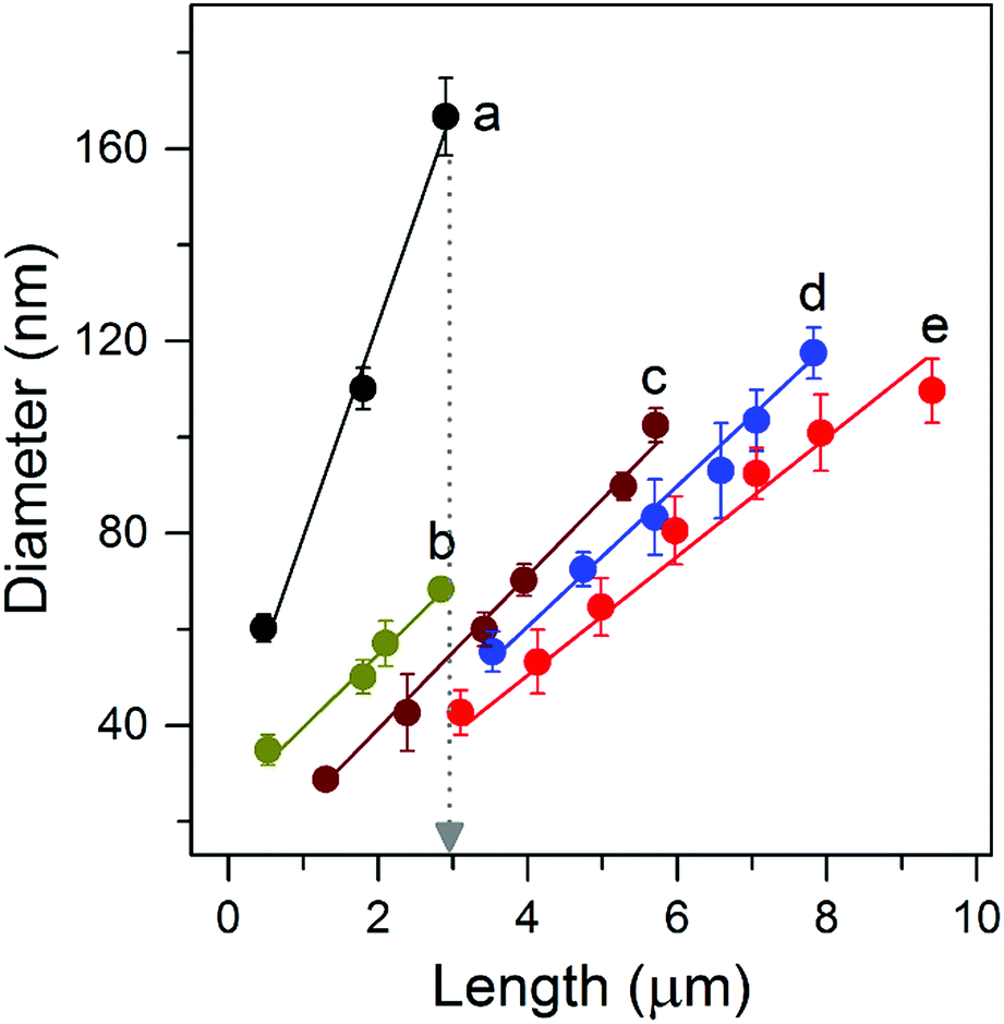 | ||
| Fig. 2 Diameter versus length of NWs grown using the indicated reaction solutions (see Table 1). Lines are fits to the data, and error bars represent one standard deviation. | ||
To increase the y/x value and suppress the lateral growth we first increased the volume ratio of HCl/DI water from 1:1 to 5:1, which increases both Cl− and H+ concentrations and thus has two main effects on the growth process. (1) Increasing the Cl− concentration can suppress the lateral growth as it can selectively be absorbed on the side facets; (2) increasing the H+ concentration can lower x in the [Ti(OH)xCly]2−complex, giving a bigger value of y and the y/x ratio. As such, the lateral growth of the NWs is significantly suppressed. The striking effect of this strategy is seen by plotting NW length versus diameter for different growth times (Fig. 2, line b). Isolated NWs with a much smaller diameter of ∼70 nm and an aspect ratio of ≈ 48 are obtained (Fig. S4b and S5b†). To further increase the y/x value polar organic solvents were used instead of DI water. In the presence of organic solvents, such as 2-butanone, some of the OH ligands in the complex will be substituted, in turn reducing x and thereby increasing the y/x ratio and suppressing the dehydration reaction in the lateral direction. As shown in Fig. 2 (lines c and d), S4 (c and d) and S5 (c and d),† the NW diameter decreased when DI water in the reaction solution was replaced with 2-butanone allowing the extended growth of high aspect ratio NWs. Subsequently, ethanol was used to replace part of the 2-butanone in order to replace the OH ligands in the complex, reduce the x number and thereby increase the y/x ratio. As expected, due to the smaller molecule size of ethanol, well-separated NWs with a much smaller diameter and a length up to ∼10 μm were obtained, see Fig. 2 (line e), S4e and 1d. The highest aspect ratio is ∼100, a value five times greater than that achieved using conventional reaction solutions.7 Our results reveal that the effective suppression of lateral NW growth during the solvothermal growth process is the key factor for obtaining long and well-separated NW arrays.
The photoelectrochemical properties of the TiO2 NW arrays
The photoelectric properties of the well-separated single-crystal TiO2 NWs were explored using intensity-modulated photocurrent spectroscopy (IMPS) and intensity-modulated photovoltage spectroscopy (IMVS) techniques.24,25Fig. 3a compares the photoelectron density (n) dependence of the electron diffusion coefficient (D) for NW and NP films. The morphology of the NP films is shown in Fig. S6.† The values of D and n were determined using procedures described in detail elsewhere.26,27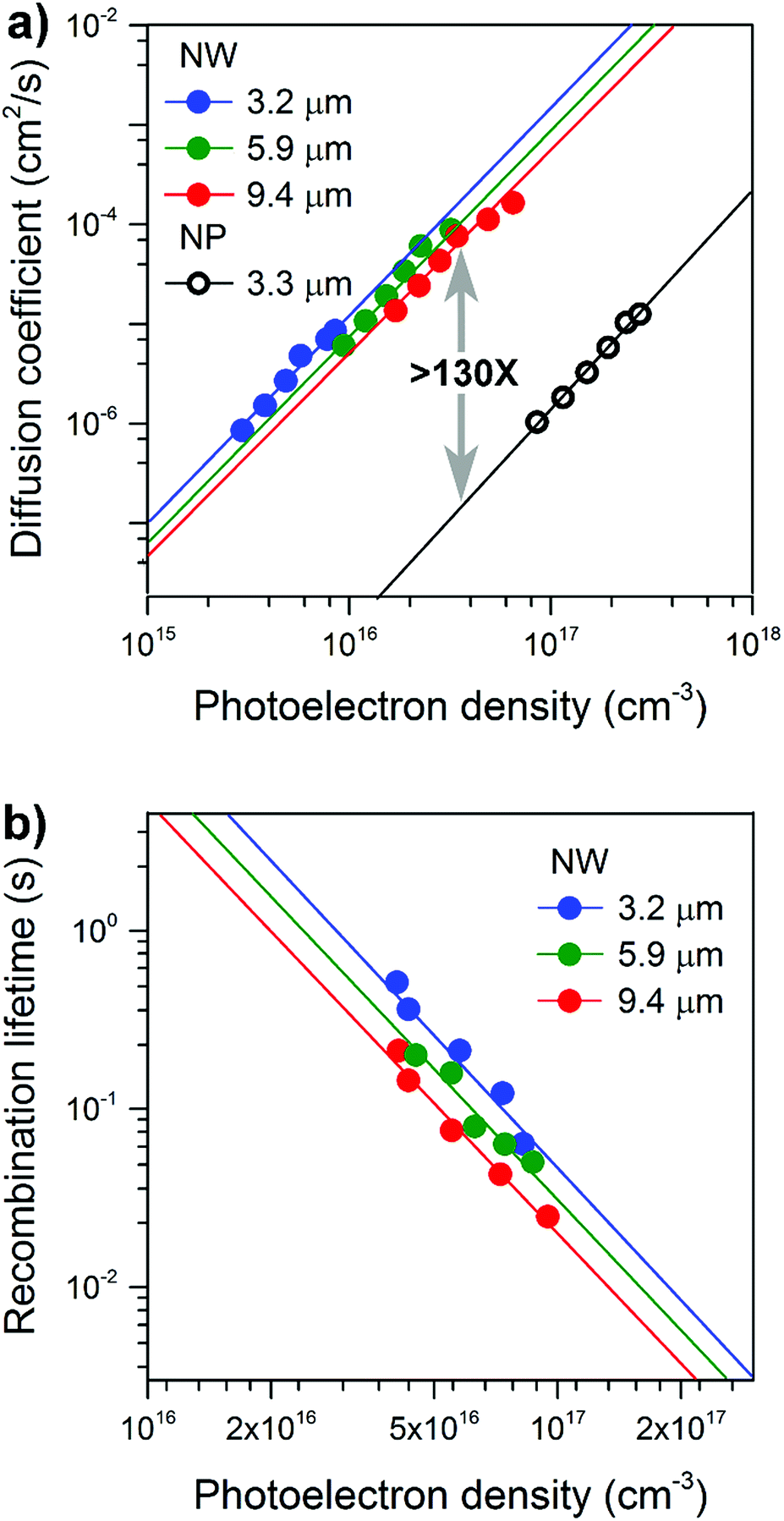 | ||
| Fig. 3 Electron transport and recombination dynamics of NW-based photoelectrodes of different thicknesses. (a) Comparison of electron diffusion coefficients as a function of the photoelectron density for NW and NP based photoelectrodes. (b) Comparison of recombination lifetimes as a function of photoelectron density for NW based photoelectrodes. | ||
The electrode D values display a power-law-dependence with n, which can be attributed to the electrons undergoing multiple trapping-detrapping events within an exponential distribution of conduction band tail states.28 Over a broad range of charge densities, as the NW length increased from 3.2 to 9.4 μm no obvious decrease in D was observed; D values are all over 100-times higher than that of the NP films. Fig. 3b compares the photoelectron density (n) dependence of the recombination time (τr) for NW array-based solar cells. Comparable electron lifetimes are recorded for NWs of different lengths and the same photoelectron density of 1017 cm−3, suggesting that the number of surface trap states is almost the same. Our results reveal excellent charge transport capabilities that are length-independent, properties we attribute to the well-separated, single-crystal nature of the NWs and long-range structural coherence.
On the basis of the transport and recombination time constants shown in Fig. 3 and S7,† the charge collection efficiency (ηcc) of NW arrays and NP films was calculated by using ηcc = 1 − τc/τr. As shown in Fig. 4a, the ηcc values of the NW arrays are all about 100%, exhibiting performance independent of film thickness (d). In contrast for the NP films there is an obvious decrease in ηcc as the film thickness increases. The independence of d and ηcc of NW arrays is of great importance to the performance of optoelectronic devices.
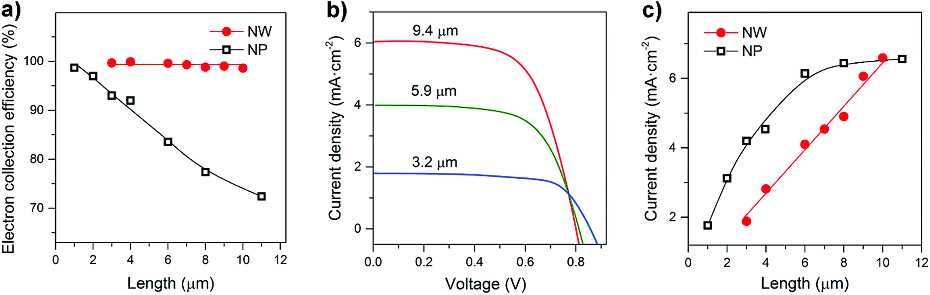 | ||
| Fig. 4 Performance of the rutile TiO2 NW and NP-based solar cells. (a) Dependence of the electron collection efficiency on the NW length and NP-film thickness. (b) Comparison of the current density–voltage characteristics of the NW-based cells under AM 1.5 illumination. (c) Dependence of current density on the NW length and NP-film thickness. | ||
Fig. 4b and S8† compare the J–V characteristics of NW and NP-based dye sensitized cells under simulated AM 1.5 light. The short circuit photocurrent density (Jsc) of the NW-based cells increases steadily with the NW length. In contrast, no obvious improvement in the NP-based cells is observed for film thicknesses greater than 6 μm. Fig. 4c presents the calibration plot of Jscversus d. In general, Jsc is determined by light-harvesting efficiency (ηlh), charge-injection efficiency (ηinj), and electron collection efficiency (ηcc). The Jsc was estimated using Jsc = qηlhηinjηccI0, where q is the elementary charge, and I0 is the incident photon flux. The ηlh value can be considered to be primarily dependent on the photoelectrode surface area,29 which was measured via dye desorption (see Fig. S9 and S10 and Tables S1 and S2†). From Fig. S11,† we can see that the surface areas of both NW and NP films increase linearly with the film thickness; since the ηcc of the NW films is independent of thickness, the Jsc value increases linearly with increasing NW length. In contrast, because the ηcc value of the NP-based cells decreases with d, their Jsc value tends to saturate as the film thickness increases. These results suggest that photoelectrodes possessing rapid charge transport properties and a charge collection efficiency independent of film thickness are of great importance to the development of high performance optoelectronic devices.
Conclusions
We have developed a simple solvothermal method for the growth of vertically aligned and well-separated single-crystal TiO2 NW arrays with a length of up to 10 μm on FTO-coated glass substrates. The effective suppression of the lateral growth is key to the NW growth process, resulting in a length to diameter ratio of approximately 100. For the first time we show a material system for which the electron transport is independent of length, leading to a 100% collection efficiency even for 10 μm thick films. This result is of great importance for the practical application of photocatalytic and electrical energy storage systems. In particular, it is an ideal basis for photoelectrode design, and application, including metal nanoparticle (QD)/NW hybrids for plasmonic water splitting, CO2 photoreduction,30 and the construction of multi-bandgap (rainbow) photovoltaics.Experimental
Preparation of TiO2 NW arrays
In a typical synthesis, the FTO coated glass substrates (Tech 7) were cleaned using DI water, acetone and ethanol. After being air dried, a TiO2 seed layer was deposited by dip-coating (0.4 M tetrabutyl titanate in ethanol) followed by 30 min heat treatment at 823 K in air. The TiO2-seeded FTO coated glass substrates were then loaded into Teflon-lined stainless-steel reactors (23 mL) filled with a solution mixture containing 1.9 mL 2-butanone, 0.1 mL ethanol, 10 mL 37% hydrochloric acid (HCl) and 1.3 mL titanium butoxide (TBOT) and kept at 443 K for a certain time. The treatments of the NW arrays were as follows: the as-grown TiO2 NW arrays were immersed in a fresh H2O2 (30 wt%)/NH3·H2O (25 wt%; v:v = 10:1) solution for 10 min and then rinsed with a copious amount of distilled water. After being dried in air, the NW arrays were annealed at 723 K for 30 min in an oxygen-rich environment with an oxygen flow rate of 0.6 L min−1 before all measurements. Finally, the rutile TiO2 NW arrays were allowed to cool to room temperature.
Conflicts of interest
There are no conflicts to declare.Acknowledgements
This research was financially supported by the National Natural Science Foundation of China (51772198 and 21501193), the Jiangsu Province Science Foundation for Distinguished Young Scholars (BK20150032), and the Project of Scientific and Technologic Infrastructure of Suzhou (SZS201708).References
- Y. Cui, Q. Wei, H. K. Park and C. M. Lieber, Science, 2001, 293, 1289–1292 CrossRef PubMed.
- M. Law, L. E. Greene, J. C. Johnson, R. Saykally and P. Yang, Nat. Mater., 2005, 4, 455–459 CrossRef PubMed.
- X. Feng, K. Shankar, M. Paulose and C. A. Grimes, Angew. Chem., Int. Ed., 2009, 48, 8095–8098 CrossRef PubMed.
- W. Zhou, X. Dai and C. M. Lieber, Rep. Prog. Phys., 2017, 80, 016701–016730 CrossRef PubMed.
- K. Shankar, J. I. Basham, N. K. Allam, O. K. Varghese, G. K. Mor, X. Feng, M. Paulose, J. A. Seabold, K. S. Choi and C. A. Grimes, J. Phys. Chem. C, 2009, 113, 6327–6359 CrossRef.
- A. I. Hochbaum, R. Fan, R. He and P. Yang, Nano Lett., 2005, 5, 457–460 CrossRef PubMed.
- B. Liu and E. S. Aydil, J. Am. Chem. Soc., 2009, 131, 3985–3990 CrossRef PubMed.
- W. Chen, V. G. Dubrovskii, X. Liu, T. Xu, R. Lardé, J. P. Nys, B. Grandidier, D. Stiévenard, G. Patriarche and P. Pareige, J. Appl. Phys., 2012, 111, 094909 CrossRef.
- X. Feng, K. Zhu, A. J. Frank, C. A. Grimes and T. E. Mallouk, Angew. Chem., Int. Ed., 2012, 51, 2727–2730 CrossRef PubMed.
- S. Hoang and P.-X. Gao, Adv. Energy Mater., 2016, 6, 1600683 CrossRef.
- Y. J. Hwang, C. Hahn, B. Liu and P. Yang, ACS Nano, 2012, 6, 5060–5069 CrossRef PubMed.
- X. Feng, K. Shankar, O. K. Varghese, M. Paulose, T. J. Latempa and C. A. Grimes, Nano Lett., 2008, 8, 3781–3786 CrossRef PubMed.
- H. S. Kim, J. W. Lee, N. Yantara, P. P. Boix, S. A. Kulkarni, S. Mhaisalkar, M. Grätzel and N.-G. Park, Nano Lett., 2013, 13, 2412–2417 CrossRef PubMed.
- J. T. Park, R. Patel, H. Jeon, D. J. Kim, J.-S. Shin and J. Hak Kim, J. Mater. Chem., 2012, 22, 6131–6138 RSC.
- H. Chen, W. Fu, H. Yang, P. Sun, Y. Zhang, L. Wang, W. Zhao, X. Zhou, H. Zhao, Q. Jing, X. Qi and Y. Li, Electrochim. Acta, 2010, 56, 919–924 CrossRef.
- A. Kumar, A. R. Madaria and C. Zhou, J. Phys. Chem. C, 2010, 114, 7787–7792 CrossRef.
- P. Sun, X. Zhang, X. Liu, L. Wang, C. Wang, J. Yang and Y. Liu, J. Mater. Chem., 2012, 22, 6389–6393 RSC.
- X. Wang, Y. Liu, X. Zhou, B. Li, H. Wang, W. Zhao, H. Huang, C. Liang, X. Yu, Z. Liu and H. Shen, J. Mater. Chem., 2012, 22, 17531–17538 RSC.
- P. Zhong, X. Chen, H. Xi, Y. Lei and X. Ma, ChemElectroChem, 2017, 4, 2783–2787 CrossRef.
- K. Zhu, T. B. Vinzant, N. R. Neale and A. J. Frank, Nano Lett., 2007, 7, 3739–3746 CrossRef PubMed.
- G. Wang, H. Wang, Y. Ling, Y. Tang, X. Yang, R. C. Fitzmorris, C. Wang, J. Zhang and Y. Li, Nano Lett., 2011, 11, 3026–3033 CrossRef PubMed.
- H. Cheng, J. Ma, Z. Zhao and L. Qi, Chem. Mater., 1995, 7, 663–671 CrossRef.
- E. Hosono, S. Fujihara, K. Kakiuchi and H. Imai, J. Am. Chem. Soc., 2004, 126, 7790–7791 CrossRef PubMed.
- L. Dloczik, O. Ileperuma, I. Lauermann, L. M. Peter, E. A. Ponomarev, G. Redmond, N. J. Shaw and I. Uhlendorf, J. Phys. Chem. B, 1997, 101, 10281–10289 CrossRef.
- G. Schlichthörl, S. Huang, J. Sprague and A. J. Frank, J. Phys. Chem. B, 1997, 101, 8141–8155 CrossRef.
- J. van de Lagemaat, N. G. Park and A. J. Frank, J. Phys. Chem. B, 2000, 104, 2044–2052 CrossRef.
- K. Zhu, N. Kopidakis, N. R. Neale, J. van de Lagemaat and A. J. Frank, J. Phys. Chem. B, 2006, 110, 25174–25180 CrossRef PubMed.
- P. J. Cameron and L. M. Peter, J. Phys. Chem. B, 2005, 109, 7392–7398 CrossRef PubMed.
- A. J. Frank, N. Kopidakis and J. van de Lagemaat, Coord. Chem. Rev., 2004, 248, 1165–1179 CrossRef.
- S. Sorcar, Y. Hwang, C. A. Grimes and S. I. In, Mater. Today, 2017, 20, 507–515 CrossRef.
Footnote |
| † Electronic supplementary information (ESI) available. See DOI: 10.1039/c8sc02335b |
| This journal is © The Royal Society of Chemistry 2018 |